AKF30N5P0SX
30V N-Channel Enhancement Mode MOSFET
General Features
➢
➢
➢
➢
➢
➢
BVDSS
Low RDS(ON)
Low Gate Charge
Advanced High Cell Density Trench Technology
RoHS Compliant
Halogen-free available
100% Avalanche Tested
RDS(ON)
@VGS=4.5V
3.9mΩ
5.2 mΩ
30V
ID
Applications
➢
➢
➢
➢
➢
RDS(ON)
@VGS=10V
59A
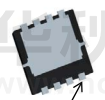
PDFN3333
High Efficiency DC/DC Converters
Synchronous Rectification
UPS Inverter
Power Management
Battery Powered System
Ordering Information
Part Number
Package
Marking
Remark
AKF30N5P0SX
PDFN3333
30N5P0SX
Halogen Free
Absolute Maximum Ratings
Symbol
TC=25℃ unless otherwise specified
Parameter
Rating
Unit
VDSS
Drain-to-Source Voltage[1]
30
V
VGSS
Gate-to-Source Voltage
±20
V
TC=25°C
59
A
TC=70°C
47
A
ID
Continuous Drain Current
IDM
Pulsed Drain Current at VGS=10V[2]
177
A
EAS
Single Pulse Avalanche Energy
(VDD=25V, VGS=10V, RG=25Ω, L=1mH)
32
mJ
PD
Power Dissipation
28
W
-55 to 150
°C
TJ and TSTG
Operating and Storage Temperature Range
Caution: Stresses greater than those listed in the “Absolute Maximum Ratings” may cause permanent damage to the device.
Thermal Characteristics
Symbol
Parameter
Rating
RθJA
Thermal Resistance, Junction-to-Ambient
45
RθJC
Thermal Resistance, Junction-to-Case
4.5
ARK Microelectronics Co., Ltd.
www.ar k- micro.com
1/9
Unit
°C /W
Rev. 1.0 Jun. 2021
�AKF30N5P0SX
Electrical Characteristics
OFF Characteristics
Symbol
TJ=25°C unless otherwise noted
Min.
Typ.
Max.
Unit
Test Conditions
Drain-to-Source Breakdown Voltage
30
--
--
V
VGS=0V, ID=250µA
IDSS
Drain-to-Source Leakage Current
--
--
1
µA
VDS=30V, VGS=0V
--
--
100
nA
VGS=20V, VDS=0V
IGSS
Gate-to-Source Leakage Current
--
--
-100
nA
VGS=-20V, VDS=0V
BVDSS
Parameter
On Characteristics
TJ=25°C unless otherwise noted
Symbol
Parameter
RDS(ON)
Static Drain-to-Source On-Resistance [3]
VGS(TH)
Gate Threshold Voltage
Min.
Typ.
Max.
Unit
Test Conditions
--
3.9
5.0
mΩ
VGS=10V, ID=8A
--
5.2
7.0
mΩ
VGS=4.5V, ID=5A
1.0
--
2.0
V
VDS = VGS, ID=250µA
Dynamic Characteristics
Symbol
Parameter
Essentially independent of operating temperature
Min.
Typ.
Max.
Ciss
Input Capacitance
--
1527
--
Coss
Output Capacitance
--
187
--
Crss
Reverse Transfer Capacitance
--
151
--
Qg
Total Gate Charge
--
33
--
Qgs
Gate-to-Source Charge
--
7.4
--
Qgd
Gate-to-Drain (Miller) Charge
--
7.1
--
Resistive Switch Characteristics
Symbol
Parameter
Min.
Typ.
Max.
Turn-on Delay Time
--
17
--
trise
Rise Time
--
51
--
td(off)
Turn-off Delay Time
--
42
--
Fall Time
--
16
--
ARK Microelectronics Co., Ltd.
Test Conditions
pF
VGS=0V
VDS=15V
f=1.0MHz
nC
VDD=15V
VGS=10V
ID=6.5A
Essentially independent of operating temperature
td(on)
tfall
Unit
www.ar k- micro.com
2/9
Unit
Test Conditions
ns
VDD=15V
VGS=10V
RG=3.3Ω
RL=2.3Ω
Rev. 1.0 Jun. 2021
�AKF30N5P0SX
Source-Drain Diode Characteristics
Symbol
Parameter
TJ=25℃ unless otherwise specified
Min.
Typ.
Max.
Unit
Test Conditions
ISD
Continuous Source Current
--
--
28
A
Maximum Ratings
VSD
Diode Forward Voltage
--
--
1.0
V
IS=1.0A,VGS=0V
NOTE:
[1] TJ=25°C to 150°C
[2] Repetitive rating, pulse width limited by maximum junction temperature.
[3] Pulse width≤380µs; duty cycle≤2%.
ARK Microelectronics Co., Ltd.
www.ar k- micro.com
3/9
Rev. 1.0 Jun. 2021
�AKF30N5P0SX
Typical Characteristics
Figure 1. On Resistance vs. Junction Temperature
Figure 2. On Resistance vs. Drain Current
10
RDS(ON),On resistance(mΩ)
RDS(ON),On resistance(Nomalized)
1.8
1.6
1.4
1.2
1
0.8
0.6
8
6
VGS=4.5V
4
VGS=10V
2
0
-50
-25
0
25
50
75
100
125
150
0
4
8
12
16
TJ,Junction Temperature(℃)
ID,Drain Current(mA)
Figure 3. Typical Capacitance vs. Drain-to-Source Voltage
Figure 4. On Resistance vs. Gate-to-Source Voltage
25
RDS(ON),On resistance(mΩ)
2500
C,Capacitance(pF)
2000
CISS
1500
1000
500
20
15
10
5
COSS
CRSS
0
0
5
0
10
15
20
0
2
4
VDS,Drain-to-Source Voltage(V)
Figure 5. Body-diode Characteristics
8
10
Figure 6. Typical Output Characteristics
100
100
VGS=10V
VGS=6V
ID,Drain Current(A)
80
IS,Source Current(A)
6
VGS,Gate-to-Source Voltage(V)
10
1
VGS=4.5V
60
40
VGS=3V
20
0.1
0
0.2
0.4
0.6
0.8
1
0
0
VSD,Source-to-Drain Voltage(V)
ARK Microelectronics Co., Ltd.
www.ar k- micro.com
4/9
1
2
3
VDS,Drain-to-Source Voltage(V)
Rev. 1.0 Jun. 2021
4
�AKF30N5P0SX
Figure 7. Typical Gate Charge vs. Gate-to-Source Voltage
1000
10
RDS(on)
Limited
6
4
100ms
DC
100
8
ID,Dranin Current(mA
VGS,Gate -to- Source Voltage(V)
Figure 8. Maximum Forward Biased Safe Operating Area
1ms
10ms
10
10s
1s
1
2
0.1
0
0.01
Ta=25℃
0
10
20
30
QG,Gate Charge(nC)
40
0.1
1
10
VDS,Drain-to-Source Voltage(V)
100
Figure 9. Normalized Thermal Transient Impedance, Junction-to-Case
Normalized Effective Transient
Thermal Impedance
10
1
50%
30%
Notes:
P
PDM
DM
10%
0.1
t1
t1
t2
t2
1.Duty Cyde.D=t1/t2
2.Per Unit Base=RθJC=4.5℃/W
3.TJM-TA=PDMZθJA
4.Surface Mounted
5%
2%
1%
Single Pulse
0.01
0.00001
0.0001
0.001
0.01
0.1
1
10
100
1000
Square Wave Pulse Duration(sec)
ARK Microelectronics Co., Ltd.
www.ar k- micro.com
5/9
Rev. 1.0 Jun. 2021
�AKF30N5P0SX
Test Circuit
VDS
ID
ID
VDS
VGS
Miller
Region
D.U.T
VGS
VDD
VGS(TH)
1mA
Qgs
Qgd
Qg
Figure 10. Gate Charge Test Circuit
Figure 11. Gate Charge Waveform
RL
VDS
VGS
D.U.T
RG
VDD
Figure 12. Resistive Switching Test Circuit
VDS
90%
10%
VGS
td(ON) trise
td(OFF) tfall
Figure 13. Resistive Switching Waveforms
ARK Microelectronics Co., Ltd.
www.ar k- micro.com
6/9
Rev. 1.0 Jun. 2021
�AKF30N5P0SX
Current
Pump
di/dt adj.
ID
Double Pluse
di/dt = 100A/uS
VDD
D.U.T
L
Qrr
ID
trr
Figure 14. Diode Reverse Recovery Test Circuit
Figure 15. Diode Reverse Recovery Waveform
BVDSS
Series Switch
(MOSFET)
IAS
L
BVDSS
D.U.T
VDD
Commutating
Diode
VGS
50Ω
IAS
VDD
0
VGS
tp
EAS =
ID
Figure 16. Unclamped Inductive Switching Test Circuit
ARK Microelectronics Co., Ltd.
tAV
2
I
L
AS
2
Figure 17. Unclamped Inductive Switching Waveforms
www.ar k- micro.com
7/9
Rev. 1.0 Jun. 2021
�AKF30N5P0SX
Package Dimensions
PDFN3333
PDFN3333
ARK Microelectronics Co., Ltd.
www.ar k- micro.com
8/9
Rev. 1.0 Jun. 2021
�AKF30N5P0SX
Published by
ARK Microelectronics Co., Ltd.
ADD: D26, UESTC National Science Park No. 1 Shuangxing Avenue, Chengdu, Sichuan.
All Rights Reserved.
Disclaimers
ARK Microelectronics Co., Ltd. reserves the right to make change without notice in order to improve
reliability, function or design and to discontinue any product or service without notice. Customers should obtain
the latest relevant information before orders and should verify that such information is current and complete. All
products are sold subject to ARK Microelectronics Co., Ltd.’s terms and conditions supplied at the time of
order acknowledgement.
ARK Microelectronics Co., Ltd. warrants performance of its hardware products to the specifications at the
time of sale, Testing, reliability and quality control are used to the extent ARK Microelectronics Co., Ltd
deems necessary to support this warrantee. Except where agreed upon by contractual agreement, testing of all
parameters of each product is not necessary performed.
ARK Microelectronics Co., Ltd. does not assume any liability arising from the use of any product or circuit
designs described herein. Customers are responsible for their products and applications using ARK
Microelectronics Co., Ltd.’s components. To minimize risk, customers must provide adequate design and
operating safeguards.
ARK Microelectronics Co., Ltd. does not warrant or convey any license either expressed or implied under its
patent rights, nor the rights of others. Reproduction of information in ARK Microelectronics Co., Ltd.’s data
sheets or data books is permissible only if reproduction is without modification or alteration. Reproduction of this
information with any alteration is an unfair and deceptive business practice. ARK Microelectronics Co., Ltd is
not responsible or liable for such altered documentation.
Resale of ARK Microelectronics Co., Ltd.’s products with statements different from or beyond the parameters
stated by ARK Microelectronics Co., Ltd. for the product or service voids all express or implied warrantees for
the associated ARK Microelectronics Co., Ltd.’s product or service and are unfair and deceptive business
practice. ARK Microelectronics Co., Ltd is not responsible or liable for any such statements.
Life Support Policy:
ARK Microelectronics Co., Ltd.’s products are not authorized for use as critical components in life devices or
systems without the expressed written approval of ARK Microelectronics Co., Ltd.
As used herein:
1. Life support devices or systems are devices or systems which:
a. are intended for surgical implant into the human body,
b. support or sustain life,
c. whose failure to perform when properly used in accordance with instructions for used provided in the
labeling, can be reasonably expected to result in significant injury to the user.
2. A critical component is any component is any component of a life support device or system whose failure
to perform can be reasonably expected to cause the failure of the life support device or system, or to affect
its safety or effectiveness.
ARK Microelectronics Co., Ltd.
www.ar k- micro.com
9/9
Rev. 1.0 Jun. 2021
�


 工商网监
湘ICP备2023018690号
工商网监
湘ICP备2023018690号
