DMX4022E/DMS4022E
Depletion-Mode Power MOSFET
eneral Features
➢
➢
➢
➢
➢
➢
Depletion Mode (Normally On)
Proprietary Advanced Planar Technology
Small Package
Low Leakage Current
RoHS Compliant
Halogen-free Available
Part Number
BVDSX
RDS(ON) (Max.)
ID
DMX4022E
400V
25Ω
0.20A
DMS4022E
400V
25Ω
0.24A
Applications
➢
➢
➢
➢
➢
➢
➢
➢
Transient Protect
Start-up
Converters
Normally On Switches
LED Drive Circuits
Power Supplies
Current Source
Voltage Source
Ordering Information
Part Number
Package
Marking
Remark
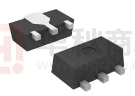
DMX4022E
SOT-89
4022
Halogen Free
DMS4022E
SOT-223
4022
Halogen Free
Absolute Maximum Ratings
Symbol
TA=25℃unless otherwise specified
Parameter
DMX4022E
[1]
DMS4022E
Unit
VDSX
Drain-to-Source Voltage
400
V
VDGX
Drain-to-Gate Voltage[1]
400
V
ID
Continuous Drain Current
0.20
0.24
IDM
Pulsed Drain Current[2]
0.80
0.96
1
1.5
W
0.008
0.012
W/℃
PD
VGS
VESD
TL
TJ and TSTG
Power Dissipation
Derating Factor above 25℃
Gate-to-Source Voltage
A
±20
V
3000
V
Source to Gate ESD[3]
3000
V
Soldering Temperature
Distance of 1.6mm from case for 10 seconds
300
Gate Source ESD
[3]
Operating and Storage Temperature Range
℃
-55 to 150
Caution: Stresses greater than those listed in the “Absolute Maximum Ratings” may cause permanent damage to the device.
Thermal Characteristics
Symbol
RθJC
Parameter
DMX4022E
Thermal Resistance, Junction-to- Case
ARK Microelectronics Co., Ltd.
125
www.ar k- micro.com
1/7
DMS4022E
83
Unit
℃/W
Rev. 2.2 Au g . 2021
�DMX4022E/DMS4022E
Electrical Characteristics
OFF Characteristics
Symbol
BVDSX
TA =25℃ unless otherwise specified
Parameter
Drain-to-Source Breakdown Voltage
ID(OFF)
Drain-to-Source Leakage Current
IGSS
Gate-to-Source Leakage Current
Min.
Typ.
Max.
Unit
Test Conditions
400
--
--
V
VGS=-5V, ID=250µA
--
--
1
µA
VDS=400V,VGS=-5V
--
--
1
mA
VDS=400V,VGS=-5V
TJ=125℃
--
--
5
--
--
-5
ON Characteristics
Symbol
IDSS
Saturated Drain-to-Source Current
RDS(ON)
Static Drain-to-Source On-Resistance
VGS(OFF)
Gate-to-Source Cut-off Voltage
gfs
Forward Transconductance
Min.
Typ.
Max.
Unit
Test Conditions
0.2
--
--
A
VGS=0V, VDS=25V[4]
--
12
25
Ω
VGS=0V,ID=200mA[4]
--
11
23
Ω
VGS=10V,ID=200mA[4]
-3.3
--
-1.5
V
VDS=3V, ID=8µA
--
193
--
mS
VDS=10V, ID=200mA[4]
Dynamic Characteristics
Parameter
Essentially independent of operating temperature
Min.
Typ.
Max.
CISS
Input Capacitance
--
103.2
COSS
Output Capacitance
--
17.7
CRSS
Reverse Transfer Capacitance
--
5.2
QG
Total Gate Charge
--
359.6
-----
QGS
Gate-to-Source Charge
--
61.6
--
QGD
Gate-to-Drain (Miller) Charge
--
130
--
Resistive Switching Characteristics
Symbol
td(ON)
trise
td(OFF)
tfall
Parameter
Unit
Test Conditions
pF
VGS=-5V
VDS=25V
f=1.0MHZ
nC
VGS=-5V~5V
VDD=100V, ID=200mA
Essentially independent of operating temperature
Min.
Typ.
Max.
Turn-on Delay Time
--
6.6
--
Rise Time
--
9.2
--
Turn-off Delay Time
--
18.8
--
Fall Time
--
356
--
Unit
Test Conditions
ns
VGS=-5V~5V
VDD=100V, ID=200mA
RG=10 Ω
Source-Drain Diode Characteristics
Symbol
VSD
VGS=-20V, VDS=0V
TA =25℃ unless otherwise specified
Parameter
Symbol
VGS=+20V, VDS=0V
µA
Parameter
Diode Forward Voltage
TA=25℃ unless otherwise specified
Min
Typ.
Max.
Units
Test Conditions
--
0.8
1.5
V
ISD=200mA[4] ,VGS=-10V
NOTE:
[1] TJ=+25℃ to +150℃
[2] Repetitive rating, pulse width limited by maximum junction temperature.
[3]The test is based on JEDEC EIA/JESD22-A114(HBM).
[4] Pulse width≤380µs; duty cycle≤2%.
ARK Microelectronics Co., Ltd.
www.ar k- micro.com
2/7
Rev. 2.2 Au g . 2021
�DMX4022E/DMS4022E
Typical Characteristics
Figure 1. Maximum Power Dissipation
vs. Case Temperature
Figure 2. Maximum Continuous Drain
Current vs. Case Temperature
Figure 3.Typical Output Characteristics
Figure 4. Typical Transfer Characteristics
Figure 5. Typical Capacitance vs.
Drain-to-Source Voltage
ARK Microelectronics Co., Ltd.
Figure 6. Typical Gate Charge vs.
Gate-to-Source Voltage
www.ar k- micro.com
3/7
Rev. 2.2 Au g . 2021
�DMX4022E/DMS4022E
Figure 7. Maximum Rated
Safe Operating Area
Figure 9. Drain-to-Source On-Resistance
vs. Junction Temperature
ARK Microelectronics Co., Ltd.
Figure 8. Drain-to-Source On-Resistance
vs. Drain Current
Figure 10. Gate-to-Source Cut-off Voltage
vs. Junction Temperature
www.ar k- micro.com
4/7
Rev. 2.2 Au g . 2021
�DMX4022E/DMS4022E
Package Dimensions
SOT-89
ARK Microelectronics Co., Ltd.
www.ar k- micro.com
5/7
Rev. 2.2 Au g . 2021
�DMX4022E/DMS4022E
SOT-223
ARK Microelectronics Co., Ltd.
www.ar k- micro.com
6/7
Rev. 2.2 Au g . 2021
�DMX4022E/DMS4022E
Published by
ARK Microelectronics Co., Ltd.
ADD: 4F, D26, UESTC National Science Park No. 1 Shuangxing Avenue, Gongxing Street,
Shuangliu District, Chengdu, China (Sichuan) Pilot Free Trade Zone.
Tel:+86-28-8523-2215
Email: sales@ark-micro.com http://www.ark-micro.com
All Rights Reserved.
Disclaimers
ARK Microelectronics Co., Ltd. reserves the right to make change without notice in order to improve
reliability, function or design and to discontinue any product or service without notice. Customers should obtain
the latest relevant information before orders and should verify that such information is current and complete. All
products are sold subject to ARK Microelectronics Co., Ltd.’s terms and conditions supplied at the time of
order acknowledgement.
ARK Microelectronics Co., Ltd. warrants performance of its hardware products to the specifications at the
time of sale, Testing, reliability and quality control are used to the extent ARK Microelectronics Co., Ltd
deems necessary to support this warrantee. Except where agreed upon by contractual agreement, testing of all
parameters of each product is not necessary performed.
ARK Microelectronics Co., Ltd. does not assume any liability arising from the use of any product or circuit
designs described herein. Customers are responsible for their products and applications using ARK
Microelectronics Co., Ltd.’s components. To minimize risk, customers must provide adequate design and
operating safeguards.
ARK Microelectronics Co., Ltd. does not warrant or convey any license either expressed or implied under its
patent rights, nor the rights of others. Reproduction of information in ARK Microelectronics Co., Ltd.’s data
sheets or data books is permissible only if reproduction is without modification or alteration. Reproduction of this
information with any alteration is an unfair and deceptive business practice. ARK Microelectronics Co., Ltd is
not responsible or liable for such altered documentation.
Resale of ARK Microelectronics Co., Ltd.’s products with statements different from or beyond the parameters
stated by ARK Microelectronics Co., Ltd. for the product or service voids all express or implied warrantees for
the associated ARK Microelectronics Co., Ltd.’s product or service and is unfair and deceptive business
practice. ARK Microelectronics Co., Ltd is not responsible or liable for any such statements.
Life Support Policy:
ARK Microelectronics Co., Ltd.’s products are not authorized for use as critical components in life devices or
systems without the expressed written approval of ARK Microelectronics Co., Ltd.
As used herein:
1. Life support devices or systems are devices or systems which:
a. are intended for surgical implant into the human body,
b. support or sustain life,
c. whose failure to perform when properly used in accordance with instructions for used provided in the
labeling, can be reasonably expected to result in significant injury to the user.
2. A critical component is any component is any component of a life support device or system whose failure
to perform can be reasonably expected to cause the failure of the life support device or system, or to affect
its safety or effectiveness.
ARK Microelectronics Co., Ltd.
www.ar k- micro.com
7/7
Rev. 2.2 Au g . 2021
�


 工商网监
湘ICP备2023018690号
工商网监
湘ICP备2023018690号
