XBLW SN74HC/HCT147
10-to-4 Line Priority Encoder
General Description
The SN74HC/HCT147 9-input priority encoders accept data from nine active LOW inputs (A0 to A8)
—
—
and provide a binary representation on the four active LOW outputs (Y0 to Y3). A priority is assigned to
each input so that when two or more inputs are simultaneously active, the input with the highest priority is
represented on the output, with input line A8 having the highest priority.
The devices provide the 10-line to 4-line priority encoding function by use of the implied decimal “zero”. The “zero”
is encoded when all nine data inputs are HIGH, forcing all four outputs HIGH.
Features
Input levels:
For SN74HC147: CMOS level
For SN74HCT147: TTL level
Encodes 10-line decimal to 4-line BCD
Useful for 10-position switch encoding
Used in code converters and generators
Specified from -40℃ to +125℃
Packaging information: DIP16/SOP16/TSSOP16
Ordering Information
Product Model
XBLW SN74HC147N
XBLW SN74HC147DTR
XBLW SN74HC147TDTR
XBLW SN74HCT147N
XBLW SN74HCT147DTR
XBLW SN74HCT147TDTR
Package Type
DIP-16
SOP-16
TSSOP-16
DIP-16
SOP-16
TSSOP-16
Marking
74HC147N
74HC147
74HC147
74HCT147N
74HCT147
74HCT147
Packing
Tube
Tape
Tape
Tube
Tape
Tape
Packing Qty
1000Pcs/Box
2500Pcs/Reel
3000Pcs/Reel
1000Pcs/Box
2500Pcs/Reel
3000Pcs/Reel
Block Diagram And Pin Description
Block Diagram
Figure 1. Logic symbol
XBLWversion1.0
www.xinboleic.com
Technical Support:4009682003
1 / 14
�XBLW SN74HC/HCT147
10-to-4 Line Priority Encoder
Figure 2. IEC logic symbol
Figure 3. Functional diagram
Figure 4. Logic diagram
Pin Configurations
XBLWversion1.0
www.xinboleic.com
Technical Support:4009682003
2 / 14
�XBLW SN74HC/HCT147
10-to-4 Line Priority Encoder
Pin Description
Pin No.
Pin Name
Description
1
A3
decimal data input (active LOW)
2
A4
decimal data input (active LOW)
3
—
A5
decimal data input (active LOW)
4
A6
decimal data input (active LOW)
5
—
A7
decimal data input (active LOW)
6
Y2
BCD address output (active LOW)
7
Y1
GND
BCD address output (active LOW)
8
ground (0V)
—
9
Y0
BCD address output (active LOW)
10
A8
decimal data input (active LOW)
11
A0
decimal data input (active LOW)
12
A1
decimal data input (active LOW)
13
A2
decimal data input (active LOW)
14
Y3
BCD address output (active LOW)
15
n.c.
16
VCC
not connected
supply voltage
Note: H=HIGH voltage level; L=LOW voltage level; X = don’t care.
Function Table
Input
Output
A0
H
A1
H
A2
H
A3
H
A4
H
A5
H
A6
H
A7
H
X
X
X
X
X
X
X
X
X
X
X
X
X
X
X
X
X
X
X
X
X
X
X
X
X
X
X
X
X
L
X
X
X
L
H
X
X
L
H
X
L
H
H
L
H
H
H
XBLWversion1.0
A8
H
Y3
H
Y2
H
Y1
H
X
L
L
H
H
L
L
H
L
H
H
H
L
H
H
H
L
L
L
L
H
H
H
H
L
L
H
H
H
H
H
H
L
H
L
H
H
H
H
H
L
H
H
H
H
H
H
H
H
H
L
L
H
H
H
H
H
H
H
L
H
H
H
H
H
H
H
H
H
L
www.xinboleic.com
Technical Support:4009682003
Y0
H
3 / 14
�XBLW SN74HC/HCT147
10-to-4 Line Priority Encoder
Electrical Parameter
Absolute Maximum Ratings
(Voltages are referenced to GND (ground=0V), unless otherwise specified.)
Parameter
Symbol
Conditions
supply voltage
VCC
Min.
-0.5
Max.
+7.0
Unit
-
input clamping
current
IIK
VI < -0.5V or VI > VCC+0.5V
-
±20
mA
output clamping
current
IOK
VO < -0.5V or VO > VCC+0.5V
-
±20
mA
output current
IO
-0.5V < VO < VCC+0.5V
±25
mA
supply current
-
ICC
-
-50
+50
mA
+150
mA
500
mW
ground current
IGND
storage temperature
Tstg
-
-65
total power
dissipation
Ptot
-
-
soldering temperature
TL
-
DIP
SOP/TSSOP
10s
Note:
[1] For DIP16 packages: above 70℃ the value of Ptot derates linearly with 12mW/K.
245
260
V
℃
℃
[2] For SOP16 packages: above 70℃ the value of Ptot derates linearly with 8mW/K.
[3] For (T)SSOP16 packages: above 60℃ the value of Ptot derates linearly with 5.5mW/K
Recommended Operating Conditions
Parameter
Symbol
Conditions
Max.
Unit
5.0
6.0
V
-
VCC
V
-
VCC
V
1.67
625
ns/V
139
ns/V
Min.
Typ.
2.0
SN74HC147
supply voltage
VCC
input voltage
VI
output voltage
VO
input transition rise
and fall rate
VCC=2.0V
Δt/ΔV
VCC=4.5V
-
VCC=6.0V
-
83
ns/V
ambient temperature
Tamb
-40
-
+125
℃
supply voltage
VCC
4.5
5.0
5.5
V
0
-
VCC
V
-
VCC
V
input voltage
VI
output voltage
VO
input transition rise
and fall rate
ambient temperature
XBLWversion1.0
-
0
-
SN74HCT147
-
0
-
-
0
Δt/ΔV
VCC=4.5V
-
1.67
139
ns/V
Tamb
-
-40
-
+125
℃
www.xinboleic.com
Technical Support:4009682003
4 / 14
�XBLW SN74HC/HCT147
10-to-4 Line Priority Encoder
Electrical Characteristics
DC Characteristics 1
(Tamb=25℃, voltages are referenced to GND (ground=0V), unless otherwise specified.)
Parameter
Conditions
Symbol
Min.
Typ.
Max.
Unit
-
V
SN74HC147
HIGH-level
input voltage
LOW-level
input voltage
HIGH-level
output voltage
LOW-level
output voltage
VIH
VIL
VOH
VCC=2.0V
1.5
1.2
VCC=4.5V
3.15
2.4
VCC=6.0V
4.2
3.2
VCC=2.0V
-
VCC=4.5V
VI=VIH or VIL
-
VI=VIH or VIL
supply current
input
capacitance
V
0.8
0.5
V
2.1
1.35
V
1.9
2.8
1.8
V
2.0
IO=-20uA; VCC=4.5V
4.5
-
V
4.4
IO=-20uA; VCC=6.0V
5.9
6.0
IO=-4.0mA; VCC=4.5V
3.98
4.32
IO=-5.2mA; VCC=6.0V
5.48
5.81
IO=20uA; VCC=2.0V
-
IO=20uA; VCC=6.0V
IO=4.0mA; VCC=4.5V
IO=5.2mA; VCC=6.0V
input leakage
current
V
VCC=6.0V
IO=-20uA; VCC=2.0V
IO=20uA; VCC=4.5V
VOL
-
-
V
V
-
V
V
0
0.1
V
0
0.1
V
0
0.1
V
0.15
0.26
V
-
0.16
0.26
V
-
II
VI=VCC or GND; VCC=6.0V
-
-
±1.0
uA
ICC
VI=VCC or GND; IO=0A; VCC=6.0V
-
-
8.0
uA
-
3.5
-
pF
CI
SN74HCT147
HIGH-level
input voltage
VIH
VCC=4.5V to 5.5V
2.0
1.6
-
V
LOW-level
input voltage
VIL
VCC=4.5V to 5.5V
-
1.2
0.8
V
HIGH-level
output voltage
VOH
VI=VIH or VIL;
VCC=4.5V
IO=-20uA
4.4
4.5
V
IO=-4.0mA
3.98
4.32
-
V
LOW-level
output voltage
VOL
VI=VIH or VIL;
VCC=4.5V
IO=20uA
-
0
0.1
V
0.26
V
input leakage
current
-
0.16
II
VI=VCC or GND; VCC=5.5V
-
-
±1.0
uA
supply current
ICC
-
-
8.0
uA
additional
supply current
ΔICC
VI=VCC or GND; IO=0A; VCC=5.5V
VI=VCC-2.1V;
other inputs at VCC or GND; IO=0A;
VCC=4.5V to 5.5V
-
100
360
uA
input
capacitance
CI
-
-
3.5
-
pF
XBLWversion1.0
IO=4.0mA
www.xinboleic.com
Technical Support:4009682003
5 / 14
�XBLW SN74HC/HCT147
10-to-4 Line Priority Encoder
DC Characteristics 2
(Tamb=-40℃ to +85℃, voltages are referenced to GND (ground=0V), unless otherwise specified.)
Parameter
Symbol
Conditions
Min.
Typ.
Max.
Unit
VCC=2.0V
1.5
3.15
-
V
VCC=4.5V
-
4.2
-
-
V
VCC=6.0V
-
-
0.5
V
VCC=2.0V
-
V
-
-
1.35
V
-
V
IO=-20uA; VCC=2.0V
1.9
1.8
4.4
-
V
IO=-20uA; VCC=4.5V
-
IO=-20uA; VCC=6.0V
5.9
-
-
IO=-4.0mA; VCC=4.5V
3.84
-
-
5.34
-
V
IO=-5.2mA; VCC=6.0V
-
-
-
0.1
V
IO=20uA; VCC=2.0V
V
-
-
0.1
V
-
-
-
-
-
SN74HC147
HIGH-level
input voltage
LOW-level
input voltage
HIGH-level
output voltage
LOW-level
output voltage
VIH
VIL
VCC=4.5V
VCC=6.0V
VOH
VI=VIH or VIL
IO=20uA; VCC=4.5V
VOL
VI=VIH or VIL
IO=20uA; VCC=6.0V
IO=4.0mA; VCC=4.5V
IO=5.2mA; VCC=6.0V
V
V
0.1
V
0.33
V
-
0.33
V
input leakage
current
II
VI=VCC or GND; VCC=6.0V
-
-
±1.0
uA
supply current
ICC
VI=VCC or GND; IO=0A; VCC=6.0V
-
-
80
uA
SN74HCT147
HIGH-level
input voltage
VIH
VCC=4.5V to 5.5V
2.0
-
-
V
LOW-level
input voltage
VIL
VCC=4.5V to 5.5V
-
-
0.8
V
HIGH-level
output voltage
VOH
VI=VIH or VIL;
VCC=4.5V
IO=-20uA
4.4
-
V
IO=-4.0mA
3.84
-
V
LOW-level
output voltage
VOL
VI=VIH or VIL;
VCC=4.5V
IO=20uA
-
-
0.1
V
-
V
input leakage
current
-
0.33
II
VI=VCC or GND; VCC=5.5V
-
-
±1.0
uA
supply current
ICC
-
-
80
uA
additional
supply current
ΔICC
VI=VCC or GND; IO=0A; VCC=5.5V
VI=VCC-2.1V;
other inputs at VCC or GND; IO=0A;
VCC=4.5V to 5.5V
-
-
450
uA
XBLWversion1.0
www.xinboleic.com
IO=4.0mA
Technical Support:4009682003
6 / 14
�XBLW SN74HC/HCT147
10-to-4 Line Priority Encoder
DC Characteristics 3
(Tamb=-40℃ to +125℃, voltages are referenced to GND (ground=0V), unless otherwise specified.)
Parameter
Symbol
Conditions
Min.
Typ.
Max.
Unit
VCC=2.0V
1.5
3.15
-
V
VCC=4.5V
-
VCC=6.0V
-
-
V
4.2
-
V
VCC=2.0V
-
-
0.5
V
-
-
1.35
V
-
V
IO=-20uA; VCC=2.0V
1.9
1.8
4.4
-
V
IO=-20uA; VCC=4.5V
-
IO=-20uA; VCC=6.0V
5.9
-
-
IO=-4.0mA; VCC=4.5V
3.7
-
-
5.2
-
V
IO=-5.2mA; VCC=6.0V
-
-
-
0.1
V
IO=20uA; VCC=2.0V
V
-
-
0.1
V
-
-
0.1
V
-
-
0.4
V
-
-
0.4
V
SN74HC147
HIGH-level
input voltage
LOW-level
input voltage
HIGH-level
output voltage
LOW-level
output voltage
VIH
VIL
VCC=4.5V
VCC=6.0V
VOH
VI=VIH or VIL
IO=20uA; VCC=4.5V
VOL
VI=VIH or VIL
IO=20uA; VCC=6.0V
IO=4.0mA; VCC=4.5V
IO=5.2mA; VCC=6.0V
V
V
input leakage
current
II
VI=VCC or GND; VCC=6.0V
-
-
±1.0
uA
supply current
ICC
VI=VCC or GND; IO=0A; VCC=6.0V
-
-
160
uA
SN74HCT147
HIGH-level
input voltage
VIH
VCC=4.5V to 5.5V
2.0
-
-
V
LOW-level
input voltage
VIL
VCC=4.5V to 5.5V
-
-
0.8
V
HIGH-level
output voltage
VOH
VI=VIH or VIL;
VCC=4.5V
-
-
V
-
V
LOW-level
output voltage
VOL
VI=VIH or VIL;
VCC=4.5V
0.1
V
input leakage
current
II
supply current
ICC
additional
supply current
ΔICC
XBLWversion1.0
IO=-20uA
4.4
IO=-4.0mA
3.7
IO=20uA
-
-
-
-
0.4
V
VI=VCC or GND; VCC=5.5V
-
-
±1.0
uA
VI=VCC or GND; IO=0A; VCC=5.5V
VI=VCC-2.1V;
other inputs at VCC or GND; IO=0A;
VCC=4.5V to 5.5V
-
-
160
uA
-
-
490
uA
www.xinboleic.com
IO=4.0mA
Technical Support:4009682003
7 / 14
�XBLW SN74HC/HCT147
10-to-4 Line Priority Encoder
AC Characteristics 2
(Tamb=-40℃ to +85℃, GND=0V, tr=tf=6ns, CL=50pF, unless otherwise specified.)
Parameter
Symbol
Conditions
Min.
Typ.
Max.
Unit
-
-
200
ns
-
-
40
ns
-
-
34
ns
-
-
95
ns
-
-
19
ns
-
-
16
ns
-
-
44
ns
-
-
19
ns
Min.
Typ.
Max.
Unit
-
-
240
ns
-
-
48
ns
-
-
41
ns
-
-
110
ns
-
-
22
ns
-
-
19
ns
-
-
53
ns
-
-
22
ns
SN74HC147
—
VCC=2.0V
—
An to Yn
propagation
delay
tpd
see Figure
6[1]
VCC=4.5V
VCC=6.0V
VCC=2.0V
transition time
tt
see Figure
6[2]
VCC=4.5V
VCC=6.0V
SN74HCT147
—
—
An to Yn
propagation
delay
tpd
transition time
tt
see Figure 6[1]
VCC=4.5V
VCC=4.5V; see Figure 6[2]
Note:
[1] tpd is the same as tPLH and tPHL.
[2] tt is the same astTHL and tTLH.
3.3.6
AC Characteristics 3
(Tamb=-40℃ to +125℃, GND=0V, tr=tf=6ns, CL=50pF, unless otherwise specified.)
Parameter
Symbol
Conditions
SN74HC147
—
VCC=2.0V
—
An to Yn
propagation
delay
tpd
see Figure 6[1]
VCC=4.5V
VCC=6.0V
VCC=2.0V
transition time
tt
see Figure 6[2]
VCC=4.5V
VCC=6.0V
SN74HCT147
—
—
An to Yn
propagation
delay
tpd
transition time
tt
see Figure 6[1]
VCC=4.5V
VCC=4.5V; see Figure 6[2]
Note:
[1] tpd is the same as tPLH and tPHL.
[2] tt is the same astTHL and tTLH
XBLWversion1.0
www.xinboleic.com
Technical Support:4009682003
8 / 14
�XBLW SN74HC/HCT147
10-to-4 Line Priority Encoder
AC Characteristics 1
(Tamb=25℃, GND=0V, tr=tf=6ns, CL=50pF, unless otherwise specified.)
Parameter
Symbol
Conditions
Min.
Typ.
Max.
Unit
-
50
160
ns
18
32
ns
15
27
ns
14
19
75
ns
7
15
ns
-
6
6
ns
-
30
-
pF
VCC=4.5V
-
20
35
ns
VCC=5.0V; CL=15pF
-
17
-
ns
-
7
15
ns
-
33
-
pF
SN74HC147
—
VCC=2.0V
—
An to Yn
propagation
delay
tpd
see Figure 6[1]
VCC=4.5V
VCC=5.0V; CL=15pF
VCC=6.0V
VCC=2.0V
transition time
tt
see Figure 6[2]
VCC=4.5V
VCC=6.0V
power
dissipation
capacitanc
e
CPD
VI=GND to VCC[3]
-
ns
SN74HCT147
—
—
An to Yn
propagation
delay
transition time
power
dissipation
capacitanc
e
tpd
see Figure 6[1]
tt
CPD
VCC=4.5V; see Figure
6[2]
VI=GND to VCC- 1.5V[3]
Note:
[1] tpd is the same as tPLH and tPHL.
[2] tt is the same astTHL and tTLH.
[3] CPD isused to determine the dynamic power dissipation (PD in uW).
PD=CPD ×VCC2 ×fi+∑(CL×VCC2 ×fo) where:
f i=input frequency in MHz;
fo=output frequency in MHz;
CL=output load capacitance in pF;
VCC=supply voltage in V;
∑(CL×VCC2×fo)=sum of outputs.
XBLWversion1.0
www.xinboleic.com
Technical Support:4009682003
9 / 14
�XBLW SN74HC/HCT147
10-to-4 Line Priority Encoder
Testing Circuit
AC Testing Circuit
Figure 5. Test circuit for measuring switching times
Definitions for test circuit:
CL=Load capacitance including jig and probe capacitance.
RT=Termination resistance should be equal to the output impedance Zo of the pulse generator. RL=Load
resistance.
S1=Test selection switch
AC Testing Waveforms
—
—
Figure 6. Input (An) to output (Yn) propagation delays and output transition times
Measurement Points
Input
Type
Output
SN74HC147
VM
VM
VX
VY
0.5×VCC
0.5×VCC
0.1×VCC
0.9×VCC
SN74HCT147
1.3V
1.3V
0.1×VCC
0.9×VCC
4.4 Test Data
Type
Input
Load
S1 position
VI
t r ,t f
CL
RL
tPLH , tPHL
SN74HC147
VCC
6ns
15pF, 50pF
1kΩ
open
SN74HCT147
3V
6ns
15pF, 50pF
1kΩ
open
XBLWversion1.0
www.xinboleic.com
Technical Support:4009682003
10 / 14
�XBLW SN74HC/HCT147
10-to-4 Line Priority Encoder
Package Information
DIP16
XBLWversion1.0
www.xinboleic.com
Technical Support:4009682003
11 / 14
�XBLW SN74HC/HCT147
10-to-4 Line Priority Encoder
SOP16
XBLWversion1.0
www.xinboleic.com
Technical Support:4009682003
12 / 14
�XBLW SN74HC/HCT147
10-to-4 Line Priority Encoder
TSSOP16
XBLWversion1.0
www.xinboleic.com
Technical Support:4009682003
13 / 14
�XBLW SN74HC/HCT147
10-to-4 Line Priority Encoder
Statement:
Shenzhen xinbole electronics co., ltd. reserves the right to change the product specifications, without notice!
Before placing an order, the customer needs to confirm whether the information obtained is the latest version,
and verify the integrity of the relevant information.
Any semiconductor product is liable to fail or malfunction under certain conditions, and the buyer shall be
responsible for complying with safety standards in the system design and whole machine manufacturing using
Shenzhen xinbole electronics co., ltd products, and take appropriate security measures to avoid the potential risk
of failure may result in personal injury or property losses of the situation occurred!
This document is for referenceonly,and the actual use should be based on the application test results.
Product performance is never ending, Shenzhen xinbole electronics co., ltd will be dedicated to provide
customers with better performance, better quality of integrated circuit products.
XBLWversion1.0
www.xinboleic.com
Technical Support:4009682003
14 / 14
�
很抱歉,暂时无法提供与“SN74HC147N”相匹配的价格&库存,您可以联系我们找货
免费人工找货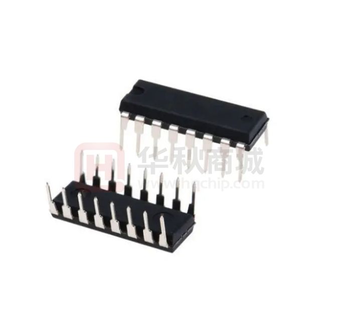


 工商网监
湘ICP备2023018690号
工商网监
湘ICP备2023018690号
