SG901-1078 ADVANCE INFORMATION
SG901-1078 Miniature Wi-Fi Radio
Overview
Features
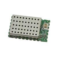
The SG901-1078 WiFi module is a shielded and
FCC certified version of the SG901-1071 Radio
Module. It is optimized to simplify successful
integration into systems requiring the latest
performance with small size. This certified
module is a highly integrated single chip based
802.11b/g/n WLAN radio for embedded, lowpower and extremely small form factor mobile
applications. The product conforms to the IEEE
802.11B, G, and N protocols operating in the
2.45GHz ISM frequency band supporting 802.11n
modulations up to 72.2Mbps, all 802.11g OFDM
modulations, and all mandatory 802.11b
modulations.
•
•
•
•
•
•
•
The SG901-1078 is a fully integrated wireless
radio including RF Synthesizer/VCO, high-speed
data converters, digital baseband processor,
onboard MAC and PHY processors, Power
Management, Power Amplifier, and LNA.
•
An on-board EEPROM stores calibration data for
alignment-free
integration.
No
customer
calibration required.
An on-board crystal and filter simplify system
integration. The addition of 1.8V, 3.3V, and VIHO
supplies, Antenna, and host communication,
provides a complete WiFi solution.
Host control is provided by either an SDIO or SPI
interface.
Shield not shown
•
•
•
•
•
•
FCC Module Certification
Small Footprint (21.3 by 13.5mm)
Factory Calibrated
RoHs Compliant
Fully Integrated 802.11 System Solution
Ultra Low Current Consumption, 2.5 m A DITM = 1
Fully Compliant with the IEEE 802.11B,G, and N
WLAN Standards
Support for 802.11n Modulations up to 72.2Mbps,
and all 802.11g and Mandatory 802.11b
Modulations
Intelligent Power Control, Including 802.11 Power
Save Mode
Supports SPI Interface and SDIO Interface
Factory Support for Linux 2.6/Android, Windows
CE
Source Code Available for porting to RTOS or
Custom OS
Hardware driver is provided under GPL
Flexible I/O Voltage
Applications
• Hand-held Devices
• Embedded Systems
• Portable Systems
• Point of Sale terminals
• Personal Digital Assistants (PDA)
• Cameras
• Cable Replacement
Ordering Information
Packaging
Temp Range
Part Number
Tape and Reel
Extended
SG901-1078-ET-TR
Bulk
Extended
SG901-1078-ET-BLK
Tape and Reel
Commercial
SG901-1078-CT-TR
Bulk
Commercial
SG901-1078-CT-BLK
Evaluation Kit Available
This EVK supports embedded software
development. Uses the SG901-1071 module.
EVK for 1071
1-321-255-0515
WWW.SAGRAD.COM
SG923-0007
DOC#: SG914-0028 rev. 1.2
�SG901-1078 ADVANCE INFORMATION
Block Diagram
1.8V
U.FL
Antenna
Connector
Timebase
3.3V
VHIO
Voltage
Supply Inputs
Power Management Unit
LNA
+Power
Amplifier
F.E.
ZIF
Transceiver
BB
Baseb and
Processo r
Processor
MAC
Host
Interface
Connection
To HOST
SPI/SDIO
High-Speed
Data
Converters
FCC Certification
Comment
FCC ID
Certified for use
with these
Antennas
Other Antennas
1-321-255-0515
TB obtained
W1038
Pulse Antennas 2.4 – 2.5 GHz with Reverse SMA connector
W1037
Pulse Antennas 2.4 – 2.5 GHz with Reverse SMA connector
MLPV2400NGP
PCTEL Ant 2.4 – 2.5 GHz with reverse SMA
13018-1
Beijing Evercommunication Ant 2.4 – 2.5 GHz with IPX
(U.FL Compatible, recommended for cost sensitive applications)
Additional Antennas may be added to the approval list at additional cost. Contact Sagrad for
additional information
WWW.SAGRAD.COM
DOC#: SG914-0028 rev. 1.2
�SG901-1078 ADVANCE INFORMATION
General Electrical Specifications
Parameter
Test Condition / Comment
Min.
Typ.
Max.
Units
Absolute Maximum Ratings
3.3V Supply
-0.3
3.6
V
VLDO Supply
-0.3
2.5
V
Operating Conditions and Input Power Specifications
Operating Temperature Range
Input Supply Voltage
3.3V Supply
Standby Mode
Current
Power Save Mode
Current
ET Version (Extended Temperature)
CT Version (Commercial Temperature)
3.3V Supply input
-30
85
°C
0
70
°C
3.6
V
2.7
32.768kHz Mode
270
uA
DTIM = 1
2.5
mA
Peak TX Current
Power Save Mode
Settling Times
VHIO Supply
3.3
270
mA
Peak RX Current
Processing Beacons
82
mA
Peak RX Current
Processing OFDM Packets
135
mA
Wake up Time
From 32.768KHz Mode
5
mS
Ramp up
To Processing Beacons
360
uS
Ramp Down
To Stand By 32.768KHz mode
760
uS
Input Supply Voltage
VHIO input supply determines Host CMOS
logic levels
1.7
3.3
V
Input Supply Current
VHIO = 1.8V
1
mA
Standby Mode
Current
VHIO = 1.8V
100
uA
VLDO Supply
Input Supply Voltage
Required Internal regulator supply input
Input Voltage
Levels
VIL
VIH
Output Voltage
Levels
VOL
IOL = 8.0mA
VOH
IOH = -8.0mA
Input Capacitance
1-321-255-0515
WWW.SAGRAD.COM
1.45
2.0
V
-0.3
0.25VHIO
V
0.625VHIO
VHIO+0.3
V
0.4
V
0.75VHIO
VHIO
V
1.0
5.0
pF
DOC#: SG914-0028 rev. 1.2
�SG901-1078 ADVANCE INFORMATION
RF Characteristics (Max and Min based on temperature range)
Parameter
Test Condition / Comment
Min.
Antenna Port Impedance
CH1 to CH14
-9.5
Maximum Input Signal
Adjacent Channel
Rejection
-14
dB
-97
-96.3
-95
dBm
11b, 2 Mbps
-94
-93.5
-91
dBm
11b, 5.5 Mbps
-93
-91
-88
dBm
11b, 11 Mbps
-89
-86.7
-85
dBm
11g, 9Mbps
-92
-89.6
-88
dBm
11g, 18Mbps
-87
-85.9
-84
dBm
11g, 36Mbps
-80
-78.6
-77
dBm
11g, 54Mbps
-74
-72.4
-70
-86
dBm
11n, MCS3
-80
dBm
11n, MCS5
-72
dBm
-69
CH1 to 14
11g, 54Mbps 10% PER
-0.7
CH7
11g, 54Mbps
-19
dBm
0.7
dB
-16
dBm
1Mbps
50
11Mbps
47
9Mbps
25
dB
54Mbps
13
dB
MCS1
24
dB
MCS7
5
dB
11b, 11Mbps
1-321-255-0515
dBm
11n, MCS1
11b, 1Mbps
TX Output Power
Units
Ohms
11b, 1Mbps
11n, MCS7
Channel to Channel
De-sensitivity
Max.
50
Antenna Input Return Loss
RX Sensitivity
Typ.
@802.11b spectral mask
15
16.5
19.1
15.5
16.2
19.4
dBm
dBm
17
18.2
19.5
dBm
11.7
13.4
15.1
dBm
11g, 9Mbps
@802.11g spectral mask
11g, 54Mbps
EVM = -27dB, 4.5%
802.11n MCS1
@802.11n spectral mask
17
dBm
802.11n MCS7
EVM = -27dB
13
dBm
WWW.SAGRAD.COM
DOC#: SG914-0028 rev. 1.2
�SG901-1078 ADVANCE INFORMATION
Pinout List
SIGNAL NAME
PIN NUMBER
DESCRIPTION
NOTES
RF Pins
2G4_RF
U.FL Connector
2G4_RF
11
Hirose Electrical PN U.FL-R-SMT(10)
Optional PAD, Factory enabled only
Careful Layout for this RF Pad and nearby ground
Serial Interface Pins (VHIO Domain, logic levels compatible with the VHIO (Pin 26) input voltage)
SDCMD
21
SPI MOSI (input)
SDIO CMD
VHIO Domain
SDCLK
22
SPI Clock Input
SDIO CLK
VHIO Domain
SDD0
20
SPI MISO (output)
SDIO Data 0
VHIO Domain
SDD1
19
SPI: Interrupt Output
SDIO Data 1
VHIO Domain
SDD2
18
SDD3
17
SPI Chip Select Input
POWERUP
4
Power Up Enable (from Host)
VLDO Domain with internal pull up High = operating,
Low = off
RSTn
25
Reset Input
VHIO Domain – Active Low reset
CLK32K
27
32.768 kHz Sleep Clock Input
VHIO Domain
VHIO
26
Supply Voltage for I/O's
1.7 to 3.3V, Internally decoupled with a 0.1uF capacitor
VLDO
9
External regulator supply input
1.45 to 2.0V, Internally decoupled with a 10uF capacitor
3.3V
8
RF PA supply
2.7 to 3.3V, Internally decoupled with a 10uF capacitor
GND
1,2,3,5,6,7,10,
12,13,14,15,16,
23,24,28,Paddle
SDIO Data 2
VHIO Domain
SDIO Data 3
VHIO Domain
Control Pins
Power and Ground Pins
1-321-255-0515
Ground Connections
WWW.SAGRAD.COM
DOC#: SG914-0028 rev. 1.2
�SG901-1078 ADVANCE INFORMATION
Software Support
The 1071 and 1078 modules are supported through highly portable software. The hardware drivers and
Wi-Fi stack as provided is compatible with Linux kernel 2.6. The source code for the hardware abstraction
is available under a GPL license and is available from Sagrad. The licensed Wi-Fi licensed stack
available from Sagrad is provided in binary form without a license. Source code for the Wi-Fi stack is
available to the customer. To obtain source code for the stack contact Sagrad sales at www.sagrad.com.
Software and source code are available free of charge but require a software license agreement for the
Wi-Fi stack source.
In almost all cases the GPL driver will need to be modified for the customer’s specific hardware. The WiFi stack will only need to be modified for compatibility to the customers OS and compiler. In many cases
such as Linux near zero modification of the Wi-Fi stack will be required.
The Wi-Fi module/stack currently is only tested in client mode and is compatible with any access point
that meets 802.11 standards. An access point mode code base is planned in the future.
The complete 802.11 stack requires about 350KB of space for the implementation of the entire
specification. Extremely small versions can be created by knowledgeable customers but is a considerable
task and requires detailed understanding of 802.11.
As a service to customers, Sagrad offers extended technical support on a fee basis.
1-321-255-0515
WWW.SAGRAD.COM
DOC#: SG914-0028 rev. 1.2
�SG901-1078 ADVANCE INFORMATION
Software Details:
MAC
■ Comprehensive MAC functionality according to IEEE 802.11-2007, including QoS traffic scheduling
■ Supports the following optional IEEE 802.11n features:
MPDU aggregation
MSDU aggregation
Immediate Block Acknowledgement
PSMP
MTBA
RIFS
L-SIG TXOP protection
Link adaptation using MCS feedback
Encryption
■ Hardware encryption according to IEEE 802.11-2007 and IEEE 802.11w/D10.0:
WEP40/64
WEP104/128
CCMP (AES)
TKIP
BIP
■ Hardware encryption support for SMS4 to support WAPI
■ Hardware encryption support for Cisco® CKIP
OS Support:
Windows Mobile 7 and 6.x, Windows CE 6.1 and 5, Linux v2.6, Android
1-321-255-0515
WWW.SAGRAD.COM
DOC#: SG914-0028 rev. 1.2
�SG901-1078 ADVANCE INFORMATION
Recommended Layout
20.25mm
2.0mm
12.5mm
8.0mm
1.6mm
Not to scale
1
NOTE: 1 Center paddle centered on
package layout.
1.57mm
10mm
2 Add maximum number of
vias for ground and thermal transfer
characteristics.
PCB design requires detailed review of the center exposed pad. This pad requires good thermal
conductivity. Soldering coverage should be maximized and checked via x-ray for proper design. There is
a trade off in providing enough solder for conductivity, and too much which allows the module to “float”
on the paddle creating reliability issues. Sagrad recommends two approaches, a large center via that
allows excess soldering to flow down into the host PCB with smaller vias around it. Or many smaller vias
with just enough space for the viscosity of the chosen solder/flux to allow some solder to flow into the
smaller vias. Each of these approaches need to result in 60% or more full contact solder coverage on the
paddle after reflow. Sagrad strongly encourages PCB layout teams to work with their EMS providers to
insure vias and solder paste designs will result in satisfactory performance.
Note: Pin one is on the bottom left of this diagram.
This view is viewed from the top.
1-321-255-0515
WWW.SAGRAD.COM
DOC#: SG914-0028 rev. 1.2
�SG901-1078 ADVANCE INFORMATION
Mechanical
TOP VIEW
BOTTOM VIEW
1-321-255-0515
WWW.SAGRAD.COM
DOC#: SG914-0028 rev. 1.2
�SG901-1078 ADVANCE INFORMATION
Packaging
The part comes packaged in Tape and Reel or bulk.
1-321-255-0515
WWW.SAGRAD.COM
DOC#: SG914-0028 rev. 1.2
�


 工商网监
湘ICP备2023018690号
工商网监
湘ICP备2023018690号

