2-Terminal IC
1.2 V Reference
AD589
FEATURES
Superior Replacement for Other 1.2 V References
Wide Operating Range: 50 A to 5 mA
Low Power: 60 W Total PD at 50 A
Low Temperature Coefficient:
10 ppm/C Max, 0C to 70C (AD589M)
2-Terminal Zener Operation
Low Output Impedance: 0.6
No Frequency Compensation Required
Low Cost
MIL-STD-883 Compliant Versions Available
FUNCTIONAL BLOCK DIAGRAMS
SOIC (R-8)
Metal Can (H-02)
��
1
8
2
7
3
6
–V 4
AD589
+V
5
TOP VIEW
(Not to Scale)
��
������ ����
PRODUCT DESCRIPTION
PRODUCT HIGHLIGHTS
The AD589 is a 2-terminal, low cost, temperature compensated
band gap voltage reference that provides a fixed 1.23 V output
voltage for input currents between 50 A and 5.0 mA.
1. The AD589 is a 2-terminal device that delivers a constant
reference voltage for a wide range of input current.
The high stability of the AD589 is primarily dependent upon
the matching and thermal tracking of the on-chip components.
Analog Devices’ precision bipolar processing and thin-film technology combine to provide excellent performance at low cost.
Additionally, the active circuit produces an output impedance 10
lower than the typical low-TC Zener diodes. This feature allows
operation with no external components required to maintain full
accuracy under changing load conditions.
The AD589 is available in seven versions. The AD589J, AD589K,
AD589L, and AD589M grades are specified for 0°C to +70°C
operation, while the AD589S and AD589T grades are rated for
the full –55°C to +125°C temperature range. All grades are available in a metal can (H-02) package. The AD589J is also available
in an 8-lead SOIC package.
2. Output impedance of 0.6 and temperature coefficients as
low as 10 ppm/°C ensure stable output voltage over a wide
range of operating conditions.
3. The AD589 can be operated as a positive or negative reference. Floating operation is also possible.
4. The AD589 will operate with a total current as low as 50 A
(60 W total power dissipation), ideal for battery-powered
instrument applications.
5. The AD589 is an exact replacement for other 1.2 V references,
offering superior temperature performance and reduced sensitivity to capacitive loading.
6. The AD589 is available in versions compliant with MILSTD-883. Consult factory for 883 data sheet.
REV. C
Information furnished by Analog Devices is believed to be accurate and
reliable. However, no responsibility is assumed by Analog Devices for its
use, nor for any infringements of patents or other rights of third parties
that may result from its use. No license is granted by implication or otherwise under any patent or patent rights of Analog Devices. Trademarks
and registered trademarks are the property of their respective owners.
One Technology Way, P.O. Box 9106, Norwood, MA 02062-9106, U.S.A.
Tel: 781/329-4700
www.analog.com
Fax: 781/326-8703
© 2004 Analog Devices, Inc. All rights reserved.
�AD589–SPECIFICATIONS (Typical @ I
IN
= 500 A and TA = 25C, unless otherwise noted.)
Model
AD589JH/
AD589JR
Min Typ Max
AD589KH
Min Typ Max
AD589LH
Min Typ Max
AD589MH
Min Typ Max
Unit
OUTPUT VOLTAGE, TA = 25°C
1.200 1.235 1.250
1.200 1.235 1.250
1.200 1.235 1.250
1.200 1.235 1.250
V
OUTPUT VOLTAGE CHANGE
VERSUS CURRENT
50 A to 5 mA
5
DYNAMIC OUTPUT IMPEDANCE
0.6
RMS NOISE VOLTAGE
10 Hz < f < 10 kHz
5
1
TEMPERATURE COEFFICIENT
5
2
0.6
2
0.6
5
25
2
0.6
5
50
100
TURN-ON SETTLING TIME TO 0.1%
5
mV
2
5
V
10
25
25
5
25
25
ppm/°C
s
OPERATING CURRENT2
0.05
5
0.05
5
0.05
5
0.05
5
mA
OPERATING TEMPERATURE
0
70
0
70
0
70
0
70
°C
3
PACKAGE OPTION
Metal Can (H-02A)
SOIC (R-8)
AD589JH
AD589JR
AD589KH
Model
AD589SH
Min Typ Max
AD589TH
Min Typ Max
Unit
OUTPUT VOLTAGE, TA = 25°C
1.200 1.235 1.250
1.200 1.235 1.250
V
OUTPUT VOLTAGE CHANGE
VERSUS CURRENT
50 A to 5 mA
5
DYNAMIC OUTPUT IMPEDANCE
0.6
RMS NOISE VOLTAGE
10 Hz < f < 10 kHz
5
1
TURN-ON SETTLING TIME TO 0.1%
OPERATING CURRENT
OPERATING TEMPERATURE
PACKAGE OPTION
Metal Can (H-02)
SOIC (R-8)
0.6
5
mV
2
5
100
TEMPERATURE COEFFICIENT
2
2
AD589MH
V
50
25
AD589LH
25
ppm/°C
s
0.05
5
0.05
5
mA
–55
+125
–55
+125
°C
3
AD589SH
AD589JR
AD589TH
NOTES
1See the Voltage Variation versus Temperature section for explanation of temperature coefficient measurement method.
2Optimum performance is obtained at currents below 500 A. For current operation below 200 A, stray shunt capacitances should be limited to 20 pF or increased to
1 F. If strays cannot be avoided, operation at 500 A and a shunt capacitor of at least 1000 pF are recommended.
3H = Hermetic Metal Can; R = SOIC.
Specifications shown in boldface are tested on all production units at final electrical test.
Specifications subject to change without notice.
–2–
REV. C
�AD589
ABSOLUTE MAXIMUM RATINGS
AD589 CHIP DIMENSIONS AND PAD LAYOUT
Current . . . . . . . . . . . . . . . . . . . . . . . . . . . . . . . . . . . . . 10 mA
Reverse Current . . . . . . . . . . . . . . . . . . . . . . . . . . . . . . . 10 mA
Power Dissipation* . . . . . . . . . . . . . . . . . . . . . . . . . . . 125 mW
Storage Temperature . . . . . . . . . . . . . . . . . . . . –65°C to +175°C
Operating Junction Temperature Range . . . . . . –55°C to +150°C
Lead Temperature (Soldering, 10 sec) . . . . . . . . . . . . . . . .300°C
�����
�������
*Absolute maximum power dissipation is limited by maximum current through the
device. Maximum rating at elevated temperatures must be computed assuming
TJ 150°C and JA = 400 = C/W.
�����
�������
��� ����� �� ��������� �� ���� ���� ���� ����� ������
��� ���������� ��������������� ������� ������� ���
��������� ������ ��� ��������
ORDERING GUIDE
Model
Temperature
Coefficient (ppm/C)
Package Description
Package Option
No. of Parts Per
Reel/Tray
Temperature
Range (C)
AD589JH
AD589JR
AD589JRZ*
AD589JR-REEL
AD589JRZ-REEL*
AD589JCHIPS
AD589KH
AD589LH
AD589MH
AD589SH
AD589SH/883B
AD589TH
AD589TH/883B
AD589TCHIPS
100
100
100
100
100
100
50
25
10
100
100
50
50
50
Metal Can (TO-51)
SOIC-8
SOIC-8
SOIC-8
SOIC-8
DICE
Metal Can (TO-51)
Metal Can (TO-51)
Metal Can (TO-51)
Metal Can (TO-51)
Metal Can (TO-51)
Metal Can (TO-51)
Metal Can (TO-51)
DICE
H-02
R-8
R-8
R-8
R-8
—
H-02
H-02
H-02
H-02
H-02
H-02
H-02
—
100
98
98
2,500
2,500
25
100
100
100
100
100
100
100
25
0 to +70
0 to +70
0 to +70
0 to +70
0 to +70
0 to +70
0 to +70
0 to +70
0 to +70
–55 to +125
–55 to +125
–55 to +125
–55 to +125
–55 to +125
*Z = Pb-free part
CAUTION
ESD (electrostatic discharge) sensitive device. Electrostatic charges as high as 4000V readily accumulate
on the human body and test equipment and can discharge without detection. Although the AD589 features
proprietary ESD protection circuitry, permanent damage may occur on devices subjected to high energy
electrostatic discharges. Therefore, proper ESD precautions are recommended to avoid performance
degradation or loss of functionality.
REV. C
–3–
�AD589
UNDERSTANDING THE SPECIFICATIONS
Voltage Variation Versus Temperature
Dynamic Performance
Many low power instrument manufacturers are becoming increasingly concerned with the turn-on characteristics of the components
being used in their systems. Fast turn-on components often enable
the end user to keep power off when not needed and yet respond
quickly when the power is turned on for operation. Figure 3 displays the turn-on characteristics of the AD589. This characteristic
is generated from cold-start operation and represents the true turnon waveform after an extended period with the supplies off. The
figure shows both the coarse and fine transient characteristics of
the device; the total settling time to within ±1 mV is about 25 s,
and there is no long thermal tail appearing after that point.
Some confusion exists in the area of defining and specifying
reference voltage error over temperature. Historically, references
have been characterized using a maximum deviation per degree
Centigrade, i.e., 10 ppm/°C. However, because of nonlinearities
in temperature characteristics, which originated in standard Zener
references (such as S type characteristics), most manufacturers
have begun to use a maximum limit error band approach to specify
devices. This technique involves measurement of the output at
3, 5, or more different temperatures to guarantee that the output
voltage will fall within the given error band. The temperature
characteristics of the AD589 consistently follows the curve shown
in Figure 1. Three-point measurement guarantees the error band
over the specified temperature range. The temperature coefficients
specified in the Specifications section represent the slopes of the
diagonals of the error band from 25°C to TMIN and 25°C to TMAX.
�����
����
����
���
��
������
������
��
������ ������� ���
��
������
Figure 3. Output Settling Characteristics
������
��
��
������
��
��
��
������
���
���
�
��
��
��
���
��
���
����������� ����
��
��
��
Figure 1. Typical AD589 Temperature Characteristics
��
��
��
��
����
��
����� �������� ������� ���� ���
��
��
��
��
Figure 4. Schematic Diagram
���
��
�
��
��
��
���
��������� ����
����
�
Figure 2. Noise Spectral Density
–4–
REV. C
�AD589
APPLICATION INFORMATION
��
The AD589 functions as a 2-terminal shunt-type regulator. It
provides a constant 1.23 V output for a wide range of input
current from 50 A to 5 mA. Figure 5 shows the simplest configuration for an output voltage of 1.2 V or less. Note that no
frequency compensation is required. If additional filtering is
desired for ultralow noise applications, minimum recommended
capacitance is 1000 pF.
�����
�����
����
��
�����
����
���
����
��� ���
��
�����
a. With 7109 12-Bit Binary ADC
��
�����
����
�����
����
Figure 5. Basic Configuration for 1.2 V or Less
��� ��
���
��� ��
The AD589 can also be used as a building block to generate
other values of reference voltage. Figure 6 shows a circuit that
produces a buffered 10 V output. Total supply current for this
circuit is approximately 2 mA.
������
�����
b. With 7107 Panel Meter ADC
Figure 7. AD589 Used as Reference for CMOS ADCs
���
����
�
The AD589 also is useful as a reference for CMOS multiplying
DACs, such as the AD7533. These DACs require a negative
reference voltage in order to provide a positive output range.
Figure 8 shows the AD589 used to supply an equivalent –1.0 V
reference to an AD7533.
�
������
�
�
����
��
����
�����
�
�
�
���
���
������
���
�
�
���
�
�
�
�
�
�
�
���
��
���
���
�����
����
�����
���
���
Figure 6. Single-Supply Buffered 10 V Reference
��
���W
The low power operation of the AD589 makes it ideal for use in
battery-operated portable equipment. It is especially useful as a
reference for CMOS analog-to-digital converters. Figure 7 shows
the AD589 used in conjunction with two popular integrating type
CMOS ADCs.
��
���
���
��
������ ������
��
�
�
����
����
�
��
����
���
������
���� �
� �� �����
Figure 8. AD589 as Reference for 10-Bit CMOS DAC
REV. C
–5–
�AD589
OUTLINE DIMENSIONS
8-Lead Standard Small Outline Package [SOIC]
Narrow Body
(R-8)
Dimensions shown in millimeters and (inches)
5.00 (0.1968)
4.80 (0.1890)
4.00 (0.1574)
3.80 (0.1497)
8
5
1
4
6.20 (0.2440)
5.80 (0.2284)
1.27 (0.0500)
BSC
0.25 (0.0098)
0.10 (0.0040)
COPLANARITY
SEATING
0.10
PLANE
0.50 (0.0196)
45
0.25 (0.0099)
1.75 (0.0688)
1.35 (0.0532)
0.51 (0.0201)
0.31 (0.0122)
8
0.25 (0.0098) 0 1.27 (0.0500)
0.40 (0.0157)
0.17 (0.0067)
COMPLIANT TO JEDEC STANDARDS MS-012AA
CONTROLLING DIMENSIONS ARE IN MILLIMETERS; INCH DIMENSIONS
(IN PARENTHESES) ARE ROUNDED-OFF MILLIMETER EQUIVALENTS FOR
REFERENCE ONLY AND ARE NOT APPROPRIATE FOR USE IN DESIGN
2-Pin Metal Header Package [TO-51]
(H-02)
Dimensions shown in inches and (millimeters)
0.230 (5.84)
DIA
0.209 (5.31)
0.10 (2.54)
45°
0.046 (1.17)
0.036 (0.91)
0.195 (4.95)
DIA
0.178 (4.52)
0.150 (3.81)
0.125 (3.17)
0.048 (1.22)
0.028 (0.71)
0.019 (0.48)
0.015 (0.38)
0.500 (12.7)
MIN
CONTROLLING DIMENSIONS ARE IN INCHES; MILLIMETERS DIMENSIONS
(IN PARENTHESES) ARE ROUNDED-OFF EQUIVALENTS FOR
REFERENCE ONLY AND ARE NOT APPROPRIATE FOR USE IN DESIGN
–6–
REV. C
�AD589
Revision History
Location
Page
2/04—Data Sheet changed from REV. B to REV. C
Changes to FEATURES . . . . . . . . . . . . . . . . . . . . . . . . . . . . . . . . . . . . . . . . . . . . . . . . . . . . . . . . . . . . . . . . . . . . . . . . . . . . . . . . . . . 1
Changes to PRODUCT DESCRIPTION . . . . . . . . . . . . . . . . . . . . . . . . . . . . . . . . . . . . . . . . . . . . . . . . . . . . . . . . . . . . . . . . . . . . . 1
Changes to PRODUCT HIGHLIGHTS . . . . . . . . . . . . . . . . . . . . . . . . . . . . . . . . . . . . . . . . . . . . . . . . . . . . . . . . . . . . . . . . . . . . . . 1
Changes to SPECIFICATIONS . . . . . . . . . . . . . . . . . . . . . . . . . . . . . . . . . . . . . . . . . . . . . . . . . . . . . . . . . . . . . . . . . . . . . . . . . . . . . 2
Added ORDERING GUIDE . . . . . . . . . . . . . . . . . . . . . . . . . . . . . . . . . . . . . . . . . . . . . . . . . . . . . . . . . . . . . . . . . . . . . . . . . . . . . . . 3
Updated OUTLINE DIMENSIONS . . . . . . . . . . . . . . . . . . . . . . . . . . . . . . . . . . . . . . . . . . . . . . . . . . . . . . . . . . . . . . . . . . . . . . . . . 6
REV. C
–7–
�–8–
C00532–0–2/04(C)
�
很抱歉,暂时无法提供与“AD589TH/883B”相匹配的价格&库存,您可以联系我们找货
免费人工找货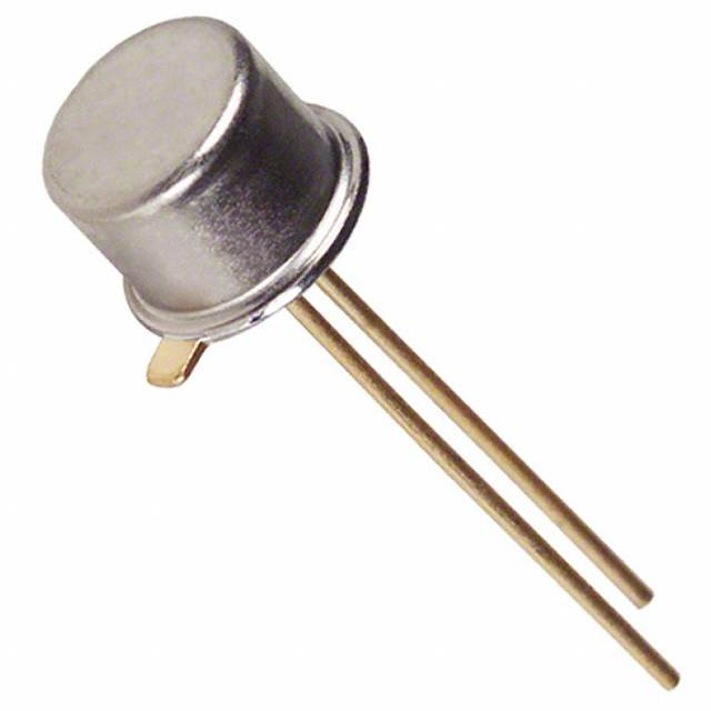


 工商网监
湘ICP备2023018690号
工商网监
湘ICP备2023018690号
