DAC5689
www.ti.com
SLLS989A – SEPTEMBER 2009 – REVISED AUGUST 2010
16-BIT, 800 MSPS 2x–8x INTERPOLATING DUAL-CHANNEL
DIGITAL-TO-ANALOG CONVERTER (DAC)
Check for Samples: DAC5689
FEATURES
DESCRIPTION
•
•
The DAC5689 is a dual-channel 16-bit 800 MSPS
digital-to-analog converter (DAC) with dual CMOS
digital data bus, integrated 2x-8x interpolation filters,
a fine frequency mixer with 32-bit complex
numerically
controlled
oscillator
(NCO),
IQ
compensation, and internal voltage reference.
Different modes of operation enable or bypass
various signal processing blocks. The DAC5689
offers superior linearity, noise and crosstalk
performance.
1
•
•
•
•
•
•
•
•
•
Dual, 16-Bit, 800 MSPS DACs
Dual, 16-Bit, 250 MSPS CMOS Input Data
– 16 Sample Input FIFO
– Flexible Input Data Bus Options
High Performance
– 81 dBc ACLR WCDMA TM1 at 70 MHz
Selectable 2x–8x Interpolation Filters
– Stop-band Attenuation > 80 dB
Complex Mixer with 32-Bit NCO
Digital Quadrature Modulator Correction
– Gain, Phase and Offset Correction
Digital Inverse SINC Filter
3- or 4-Wire Serial Control Interface
On Chip 1.2-V Reference
Differential Scalable Output: 2 to 20 mA
Package: 64-pin 9×9mm QFN
The DAC5689 dual CMOS data bus provides 250
MSPS input data transfer per DAC channel. Several
input data options are available: dual-bus data,
single-bus interleaved data, even and odd
multiplexing at half-rate, and an input FIFO with either
external or internal clock to ease interface timing.
Input data can be interpolated 2x, 4x or 8x by
on-board digital interpolating FIR filters with over 80
dB of stop-band attenuation.
The DAC5689 allows both complex or real output. An
optional 32-bit NCO/mixer in complex mode provides
frequency upconversion and the dual DAC output
produces a complex Hilbert Transform pair. A digital
Inverse SINC filter compensates for the natural DAC
sin(x)/x frequency roll-off. The digital Quadrature
Modulator Correction (QMC) feature allows IQ
compensation of phase, gain and offset to maximize
sideband rejection and minimize LO feed-through of
an external quadrature modulator performing the final
single sideband RF up-conversion.
APPLICATIONS
•
•
•
•
•
Cellular Base Stations
Broadband Wireless Access (BWA)
WiMAX 802.16
Fixed Wireless Backhaul
Cable Modem Termination System (CMTS)
The DAC5689 is pin upgradeable to the DAC5688
which includes a clock multiplying PLL. The DAC5689
is characterized for operation over the industrial
temperature range of -40°C to 85°C and is available
in a 64-pin 9x9mm QFN package.
ORDERING INFORMATION (1)
(1)
(2)
(3)
(4)
ORDER CODE
TA = –40°C to 85°C
PACKAGE QTY
TAPE AND REEL FORMAT
DAC5689IRGCT
250
DAC5689IRGCR
2000
(2)
PACKAGE
DRAWING/TYPE (3)
(4)
RGC / 64QFN
Quad FlatpackNo-Lead
For correct DAC5689 operation, bits [1:0] in register CONFIG26 need to be set to "10" at device startup (see Recommended Startup
Sequence).
For the most current package and ordering information, see the Package Option Addendum at the end of this document, or see the TI
website at www.ti.com.
Thermal Pad Size: 7,4 mm × 7,4 mm
MSL Peak Temperature: Level-3-260C-168 HR
1
Please be aware that an important notice concerning availability, standard warranty, and use in critical applications of Texas
Instruments semiconductor products and disclaimers thereto appears at the end of this data sheet.
PRODUCTION DATA information is current as of publication date.
Products conform to specifications per the terms of the Texas
Instruments standard warranty. Production processing does not
necessarily include testing of all parameters.
Copyright © 2009–2010, Texas Instruments Incorporated
�DAC5689
SLLS989A – SEPTEMBER 2009 – REVISED AUGUST 2010
www.ti.com
This integrated circuit can be damaged by ESD. Texas Instruments recommends that all integrated circuits be handled with
appropriate precautions. Failure to observe proper handling and installation procedures can cause damage.
ESD damage can range from subtle performance degradation to complete device failure. Precision integrated circuits may be more
susceptible to damage because very small parametric changes could cause the device not to meet its published specifications.
FUNCTIONAL BLOCK DIAGRAM
VFUSE
CLKVDD
DVDD
CLK2
CLK2C
CLKOUT
1.2 V
Reference
Internal Clock Generation
2-8x Fdata
CLKO_CLK1
BIASJ
CLK1C
A
QMC
gain
A-Offset
SYNC
TXENABLE
FIR2
FIR4
DA[15:0]
Input FIFO /
Demux
x2
x2
x2
2x – 8x Interpolation
67 taps
DB[15:0]
x2
19 taps
11 taps
x2
x2
Quadrature Modulator
Correction (QMC):
Phase & Gain
FIR3
Full Mixer (FMIX)
FIR1
x
sin(x)
SDIO SDO SDENB SCLK
IOUTA1
IOUTA2
9 taps
x
sin(x)
16-b DAC
IOUTB1
IOUTB2
QMC
B-Offset
32-bit NCO
SIF Control
16-b DAC
sin
cos
RESETB
EXTIO
EXTLO
IOVDD
B
gain
AVDD
GND
2
DVDD
RESETB
50
49
51
IOUTA2
IOUTA1
AVDD
AVDD
52
AVDD
55
54
53
BIASJ
EXTIO
57
56
AVDD
EXTLO
59
58
IOUTB1
IOUTB2
60
AVDD
62
61
NC
DVDD
64
63
PINOUT
CLKVDD
1
48
SDENB
CLK2
2
47
SCLK
CLK2C
3
46
SDIO
GND
4
45
SDO
SYNC
5
44
VFUSE
TXENABLE
DA15
6
43
DB15
42
DB14
DA14
8
41
DB13
IOVDD
9
40
DB12
DVDD
10
39
DVDD
DA13
11
38
DB11
DA12
12
37
DB10
DA11
13
36
DB9
DA10
14
35
DB8
DA9
15
34
DB7
DA8
16
33
DB6
DAC5689
7
26
27
28
29
30
31
32
CLK1C
DB0
DB1
DB2
DB3
DB4
DB5
24
25
DA0
CLKO_CLK1
22
23
DA1
21
DA3
DA2
19
20
DA5
DA6
DA4
17
18
DA7
RGC Package
64QFN, 9x9mm
(Top View)
Submit Documentation Feedback
Copyright © 2009–2010, Texas Instruments Incorporated
Product Folder Link(s): DAC5689
�DAC5689
www.ti.com
SLLS989A – SEPTEMBER 2009 – REVISED AUGUST 2010
TERMINAL FUNCTIONS
TERMINAL
I/O
DESCRIPTION
NAME
NO.
AVDD
51, 54, 55,
59, 62
I
Analog supply voltage. (3.3V)
BIASJ
57
O
Full-scale output current bias. For 20mA full-scale output current, connect a 960 Ω resistor to GND.
CLK2
2
I
Positive DAC clock input. Accepts frequencies up to 800MHz.
CLK2C
3
I
Complementary CLK2 input.
25
In Dual Clock Mode can be used to provide the lower frequency input clock. The lower frequency
clock can be differential or single-ended. If single-ended CLK1 can be used as the clock input.
I/O
CLK1C must be AC coupled to GND in this case. Optionally provides (CLKO) output for data bus
source. Internal pull-down.
CLK1C
26
In Dual Clock Mode can be used to provide the lower frequency input clock. The lower frequency
clock can be differential or single-ended. If differential, CLK1C is the complementary clock input. If
I/O
single-ended it can be used as the clock input. CLKO_CLK1 must be AC coupled to GND in this
case. Internal pull-down.
CLKVDD
1
CLKO_CLK1
I
Internal clock buffer supply voltage. (1.8V)
It is recommended to isolate this supply from DVDD.
I
A-Channel Data Bits 0 through 15.
DA15 is most significant data bit (MSB) – pin 7
DA0 is least significant data bit (LSB) – pin 24
Internal pull-down. The order of bus can be reversed via CONFIG4 reva bit.
DA[15..0]
7, 8, 11–24
DB[15..0]
40–43,
27–38
I
B-Channel Data Bits 0 through 15.
DB15 is most significant data bit (MSB) – pin 43
DB0 is least significant data bit (LSB) – pin 27
Internal pull-down. The order of bus can be reversed via CONFIG4 revb bit.
DVDD
10, 39, 50,
63
I
Digital supply voltage. (1.8V)
For best performance it is recommended to isolate pins 10 and 39 from all other 1.8V supplies.
EXTIO
56
Used as external reference input when internal reference is disabled (i.e., EXTLO connected to
I/O AVDD). Used as internal reference output when EXTLO = GND, requires a 0.1mF decoupling
capacitor to GND when used as reference output
EXTLO
58
O
Connect to GND for internal reference, or AVDD for external reference.
4,
Thermal
Pad
I
Pin 4 and the Thermal Pad located on the bottom of the QFN package is ground for AVDD, DVDD
and IOVDD supplies.
GND
IOUTA1
52
O
A-Channel DAC current output. An offset binary data pattern of 0x0000 at the DAC input results in a
full scale current sink and the least positive voltage on the IOUTA1 pin. Similarly, a 0xFFFF data
input results in a 0 mA current sink and the most positive voltage on the IOUTA1 pin. In single DAC
mode, outputs appear on the IOUTA1/A2 pair only.
IOUTA2
53
O
A-Channel DAC complementary current output. The IOUTA2 has the opposite behavior of the
IOUTA1 described above. An input data value of 0x0000 results in a 0mA sink and the most positive
voltage on the IOUTA2 pin.
IOUTB1
61
O
B-Channel DAC current output. Refer to IOUTA1 description above.
IOUTB2
60
O
B-Channel DAC complementary current output. Refer to IOUTA2 description above.
IOVDD
9
I
3.3V supply voltage for all digital I/O. Note: This supply input should remain at 3.3V regardless of the
1.8V or 3.3V selectable digital input switching thresholds via CONFIG26 io_1p8_3p3.
NC
64
I
No connect. Leave open for proper operation.
SYNC
5
I
Optional SYNC input for internal clock dividers, FIFO, NCO and QMC blocks. Internal pull-down.
RESETB
49
I
Resets the chip when low. Internal pull-up.
SCLK
47
I
Serial interface clock. Internal pull-down.
SDENB
48
I
Active low serial data enable, always an input to the DAC5689. Internal pull-up.
SDIO
46
I/O
Bi-directional serial data in 3-pin mode (default). In 4-pin interface mode (CONFIG5 sif4), the SDIO
pin is an input only. Internal pull-down.
SDO
45
O
Uni-directional serial interface data in 4-pin mode (CONFIG5 sif4). The SDO pin is 3-stated in 3-pin
interface mode (default). Internal pull-down.
TXENABLE
6
I
Transmit enable input. Internal pull-down. TXENABLE must be high for the DATA to the DAC to be
enabled. When TXENABLE is low, the digital logic section is forced to all 0, and any input data is
ignored.
Submit Documentation Feedback
Copyright © 2009–2010, Texas Instruments Incorporated
Product Folder Link(s): DAC5689
3
�DAC5689
SLLS989A – SEPTEMBER 2009 – REVISED AUGUST 2010
www.ti.com
TERMINAL FUNCTIONS (continued)
TERMINAL
NAME
NO.
VFUSE
44
I/O
I
DESCRIPTION
Digital supply voltage. (1.8V) This supply pin is also used for factory fuse programming. Connect to
DVDD pins for normal operation.
ABSOLUTE MAXIMUM RATINGS
over operating free-air temperature range (unless otherwise noted) (1)
Supply voltage range
DVDD
VALUE
UNIT
–0.5 to 2.3
V
VFUSE (2)
–0.5 to 2.3
V
CLKVDD (2)
–0.5 to 2.3
V
AVDD
Supply voltage range
(2)
(2)
–0.5 to 4
V
IOVDD (2)
–0.5 to 4
V
AVDD to DVDD
–2 to 2.6
V
–0.5 to 0.5
V
IOVDD to AVDD
–0.5 to 0.5
V
CLK2, CLK2C (2)
–0.5 to CLKVDD + 0.5
V
–0.5 to IOVDD + 0.5
V
–0.5 to IOVDD + 0.5
V
–0.5 to IOVDD + 0.5
V
–0.5 to AVDD + 0.5
V
CLKVDD to DVDD
CLKO_CLK1, CLK1C, SLEEP, TXENABLE (2)
DA[15..0] ,DB[15..0]
(2)
SDO, SDIO, SCLK, SDENB, RESETB
IOUTA1/B1, IOUTA2/B2
EXTIO, EXTLO, BIASJ
(2)
(2)
(2)
Peak input current (any input)
Peak total input current (all inputs)
–0.5 to AVDD + 0.5
V
20 mA
mA
–30 mA
mA
Operating free-air temperature range, TA: DAC5689I
–40 to 85
°C
Storage temperature range
–65 to 150
°C
(1)
(2)
Stresses beyond those listed under absolute maximum ratings may cause permanent damage to the device. These are stress ratings
only, and functional operation of these or any other conditions beyond those indicated under recommended operating conditions is not
implied. Exposure to absolute-maximum-rated conditions for extended periods may affect device reliability.
Measured with respect to GND.
THERMAL INFORMATION
over operating free-air temperature range (unless otherwise noted)
DAC5689
THERMAL METRIC
RGC
UNITS
64 LEAD
qJA
Theta junction-to-ambient (still air)
22
Theta junction-to-ambient (150 lfm)
15
qJB
Theta junction-to-board
TJ
Maximum junction temperature (1)
yJT
Psi junction-to-top of package
(1)
(2)
4
3.5
(2)
°C/W
°C/W
125
°C
0.2
°C/W
Air flow or heat sinking reduces qJA and may be required for sustained operation at 85°C under maximum operating conditions.
It is strongly recommended to solder the device thermal pad to the board ground plane.
Submit Documentation Feedback
Copyright © 2009–2010, Texas Instruments Incorporated
Product Folder Link(s): DAC5689
�DAC5689
www.ti.com
SLLS989A – SEPTEMBER 2009 – REVISED AUGUST 2010
ELECTRICAL CHARACTERISTICS (DC Specifications)
over recommended operating free-air temperature range, AVDD, IOVDD = 3.3 V, DVDD, CLKVDD = 1.8 V, IoutFS = 20 mA
PARAMETER
TEST CONDITIONS
RESOLUTION
MIN
TYP
MAX
UNIT
16
Bits
DC ACCURACY
INL
Integral nonlinearity
DNL
Differential nonlinearity
1 LSB = IOUTFS/216
±4
LSB
±2
LSB
ANALOG OUTPUT
Coarse gain linearity
± 0.04
Offset error mid code offset
Gain error
%FSR
With external reference
1
%FSR
With internal reference
0.7
Gain mismatch
With internal reference, dual DAC mode
Minimum full scale output current
Nominal full-scale current, IOUTFS = 16 × IBIAS current.
–2
%FSR
2
%FSR
2
Maximum full scale output current
Output compliance range (1)
LSB
0.01
mA
20
IOUTFS = 20 mA
AVDD
– 0.5V
Output resistance
Output capacitance
AVDD
+ 0.5V
V
300
kΩ
5
pF
REFERENCE OUTPUT
VREF
Reference output voltage
Internal Reference Mode
1.14
Reference output current (2)
1.2
1.26
V
100
nA
REFERENCE INPUT
VEXTIO
Input voltage range
External Reference Mode
0.1
Input resistance
Small signal bandwidth
1.25
V
1
CONFIG26: isbiaslpf_a and isbiaslpf_b = 0
95
CONFIG26: isbiaslpf_a and isbiaslpf_b = 1
472
Input capacitance
MΩ
kHz
100
pF
TEMPERATURE COEFFICIENTS
Offset drift
Gain drift
±1
With external reference
±15
With internal reference
±30
Reference voltage drift
ppm of
FSR/°C
±8
ppm/°C
POWER SUPPLY
PSRR
AVDD, IOVDD
3.0
3.3
3.6
DVDD, CLKVDD
1.7
1.8
1.9
V
0.2
%FSR/V
Power supply rejection ratio
DC tested
AVDD + IOVDD current, 3.3V
Mode 1: ×8 Interp, QMC = off, ISINC = off,
DAC A+B on, FIN = 5 MHz Tone, NCO = 145 MHz,
FOUT = 150 MHz, FDAC = 500 MHz
DVDD + CLKVDD current, 1.8V
–0.2
Power Dissipation
AVDD + IOVDD current, 3.3V
DVDD + CLKVDD current, 1.8V
P
Mode 2: ×8 Interp, QMC = on, ISINC = on,
DAC A+B on, FIN = 5 MHz Tone, NCO = 91 MHz
FOUT = 96 MHz, FDAC = 614.4 MHz
Power dissipation
AVDD + IOVDD current, 3.3V
DVDD + CLKVDD current, 1.8V
Mode 3 (Max): ×4 Interp, QMC = on, ISINC = on,
DAC A+B on, FIN = 5 MHz Tone, NCO = 135 MHz,
FOUT = 140 MHz, FDAC = 800 MHz
Power dissipation
AVDD + IOVDD current, 3.3V
DVDD + CLKVDD current, 1.8V
Power dissipation
(1)
(2)
140
mA
430
mA
1240
mW
140
mA
520
mA
1400
mW
140
mA
680
1690
Mode 4 (Sleep): ×8 Interp, QMC = off, ISINC = off,
DAC A+B off, FIN = 5 MHz Tone, NCO = off,
FOUT = off, FDAC = 800 MHz,
V
mA
1950
12
mA
15
65
mW
mA
100
mW
The upper limit of the output compliance is determined by the CMOS process. Exceeding this limit may result in transistor breakdown,
resulting in reduced reliability of the DAC5689 device. The lower limit of the output compliance is determined by the load resistors and
full-scale output current. Exceeding the upper limit adversely affects distortion performance and integral nonlinearity.
Use an external buffer amplifier with high impedance input to drive any external load.
Submit Documentation Feedback
Copyright © 2009–2010, Texas Instruments Incorporated
Product Folder Link(s): DAC5689
5
�DAC5689
SLLS989A – SEPTEMBER 2009 – REVISED AUGUST 2010
www.ti.com
ELECTRICAL CHARACTERISTICS (AC Specifications)
Over recommended operating free-air temperature range, AVDD, IOVDD = 3.3 V, DVDD, CLKVDD = 1.8 V, IOUTFS = 20 mA
PARAMETER
TEST CONDITIONS
MIN
TYP
MAX
UNIT
ANALOG OUTPUT (1)
fDAC
Maximum output update rate
ts(DAC)
Output settling time to 0.1%
Transition: Code 0x0000 to 0xFFFF
tpd
Output propagation delay
DAC outputs are updated on falling edge of DAC clock.
Does not include Digital Latency (see below).
tr(IOUT)
Output rise time
tf(IOUT)
Output fall time
Digital latency
AC PERFORMANCE
SFDR
SNR
IMD
ns
2
ns
10% to 90%
220
ps
90% to 10%
220
ps
No Interp, NCO off, QMC off, ISINC = off
109
x2 Interpolation, NCO off, QMC off, ISINC = off
172
x4 Interpolation, NCO off, QMC off, ISINC = off
276
x8 Interpolation, NCO off, QMC off, ISINC = off
488
x8 Interpolation, NCO on, QMC off, ISINC = off
512
x8 Interpolation, NCO on, QMC on, ISINC = off
528
x8 Interpolation, NCO on, QMC on, ISINC = on
548
Spurious free dynamic
range
×4 Interp, CLK2 = 800 MHz,
DAC A+B on,
0 dBFS Single tone, FOUT = FIN
First Nyquist Zone < fDATA/2
×4 Interp, CLK2 = 800 MHz,
DAC A+B on,
0 dBFS Single tone, FIN = 10.1 MHz,
FOUT = FIN + NCO
(3)
79
NCO= 10 MHz, FOUT= 20.1 MHz
72
NCO= 60 MHz, FOUT= 70.1 MHz
68
NCO= 140 MHz, FOUT= 150.1 MHz
64
NCO= 290 MHz, FOUT= 300.1 MHz
57
NCO= 40 MHz, FOUT= 51±0.5 MHz
85
NCO= 60 MHz, FOUT= 71±0.5 MHz
83
NCO= 130 MHz, FOUT= 141±0.5 MHz
74
Four-tone Intermodulation
to Nyquist
(Each tone at –12 dBFS)
×4 Interp, CLK2 = 800 MHz, DAC A+B on,
FIN = 9.8, 10.4, 11.6 and 12.2 MHz (600kHz spacing), NCO = 129 MHz,
FOUT = FIN + NCO = 140±1.2 MHz
Adjacent channel
leakage ratio
(3)
6
83
FOUT= 20.1 MHz
Third-order
Two-Tone intermodulation
(Each tone at –6 dBFS)
Noise floor,
noise spectral density
(NSD)
(1)
(2)
(3)
FOUT= 10.1 MHz
×4 Interp, CLK2 = 800 MHz,
DAC A+B on,
FIN = 10.5 and 11. 5 MHz,
FOUT = FIN + NCO
×8 Interp, CLK2 = 737.28 MHz,
DAC A+B on, FIN = 23 .04 MHz, NCO = off
ACLR
MSPS
10.4
DAC
clock
cycles
(2)
Signal-to-noise ratio
IMD3
800
×8 Interp, CLK2 = 737.28 MHz,
DAC A+B on, FIN = Baseband I/Q,
FOUT = NCO
×8 Interp, CLK2 = 737.28 MHz,
DAC A+B on,
FIN = FOUT = Baseband I/Q,
50 MHz offset, 1 MHz BW
73
Single Carrier, FOUT = 23.04 MHz
81
Single Carrier, FOUT = 70MHz
81
Single Carrier, FOUT = 140MHz
78
dBc
dBc
dBc
dBc
dBc
Four Carrier, FOUT = 140MHz
70
Single Carrier Noise Floor
101
dBm
Single Carrier NSD in 1 MHz BW
161
dBm/Hz
Four Carrier Noise Floor
101
dBm
Four Carrier NSD in 1 MHz BW
161
dBm/Hz
Measured differential across IOUTA1 and IOUTA2 or IOUTB1 and IOUTB2 with 25 Ω each to AVDD.
4:1 transformer output termination, 50Ω doubly terminated load
W-CDMA with 3.84 MHz BW, 5-MHz spacing, centered at IF. TESTMODEL 1, 10 ms
Submit Documentation Feedback
Copyright © 2009–2010, Texas Instruments Incorporated
Product Folder Link(s): DAC5689
�DAC5689
www.ti.com
SLLS989A – SEPTEMBER 2009 – REVISED AUGUST 2010
ELECTRICAL CHARACTERISTICS (Digital Specifications)
Over recommended operating free-air temperature range, AVDD, IOVDD = 3.3V, DVDD, CLKVDD = 1.8V, IoutFS = 20 mA
PARAMETER
TEST CONDITIONS
MIN
TYP
MAX
UNIT
CMOS INTERFACE: SDO, SDIO, SCLK, SDENB, RESETB, DA[15:0], DB[15:0], SYNC, TXENABLE, CLKO_CLK1
CONFIG26 io_1p8_3p3 = 0 (3.3V levels)
2.30
CONFIG26 io_1p8_3p3 = 1 (1.8V levels)
1.25
VIH
High-level input voltage
VIL
Low-level input voltage
IIH
High-level input current
±20
mA
IIL
Low-level input current
±20
mA
CI
CMOS Input capacitance
2
pF
VOH
VOL
V
CONFIG26 io_1p8_3p3 = 0 (3.3V levels)
1.00
CONFIG26 io_1p8_3p3 = 1 (1.8V levels)
0.54
SDO, SDIO, CLKO
ILOAD = –100 mA
SDO, SDIO, CLKO
ILOAD = –2 mA
SDO, SDIO, CLKO
ILOAD = 100 mA
0.2
SDO, SDIO, CLKO
ILOAD = 2 mA
0.5
Input data rate
V
IOVDD –
0.2
V
0.8 ×
IOVDD
0
250
V
MSPS
ts(SDENB)
Setup time, SDENB to rising edge of SCLK
20
ns
ts(SDIO)
Setup time, SDIO valid to rising edge of SCLK
10
ns
th(SDIO)
Hold time, SDIO valid to rising edge of SCLK
5
ns
tSCLK
Period of SCLK
100
ns
tSCLKH
High time of SCLK
40
ns
tSCLK
Low time of SCLK
40
td(Data)
Data output delay after falling edge of SCLK
10
ns
tRESET
Minimum RESETB pulse width
25
ns
ns
TIMING PARALLEL DATA INPUT TO CLK1/C (DUAL CLOCK and DUAL SYNCHRONOUS CLOCK MODES: Figure 28)
ts
Setup time
th
Hold time
t_align
Max timing offset between CLK1 and CLK2
rising edges
CLK1/C = input
DUAL SYNCHRONOUS BUS MODE only
(Typical characteristic)
1
ns
1
ns
1
- 0.55
ns
2fCLK 2
TIMING PARALLEL DATA INPUT TO CLKO (EXTERNAL CLOCK MODE: Figure 29)
ts
Setup time
th
Hold time
td(CLKO)
Delay time
1
CLKO_CLK1 = output. Note: Delay time
increases with higher capacitive loads.
ns
1
ns
4.5
ns
CLOCK INPUT (CLK2/CLK2C)
CLK2/C Duty cycle
40%
CLK2/C Differential voltage (1)
60%
0.4
CLK2/C Input common mode
1
V
2/3 × CLKVDD
CLK2C Input Frequency
V
800
MHz
CLOCK INPUT (CLK1/CLK1C)
CLK1/C Duty cycle
40%
CLK1/C Differential voltage
0.4
CLK1/C Input common mode
60%
1.0
V
IOVDD / 2
CLK1/C Input Frequency
V
250
MHz
185
MHz
CLOCK OUTPUT (CLKO)
CLKO Output frequency (2)
(1)
(2)
with 10pF load
Driving the clock input with a differential voltage lower than 1V will result in degraded performance.
Specified by design and simulation. Not production tested. It is recommended to buffer CLKO.
Submit Documentation Feedback
Copyright © 2009–2010, Texas Instruments Incorporated
Product Folder Link(s): DAC5689
7
�DAC5689
SLLS989A – SEPTEMBER 2009 – REVISED AUGUST 2010
www.ti.com
TYPICAL CHARACTERISTICS
Figure 1. Integral Nonlinearity
Figure 2. Differential Nonlinearity
10
10
Fdata = 200 MSPS, IQ
FIN = 20 MHz Complex
IF = 20 MHz
x4 Interpolation
0
-10
-10
-20
Power - dBm
Power - dBm
-20
-30
-40
-50
-30
-40
-50
-60
-60
-70
-70
-80
-80
-90
Fdata = 200 MSPS, IQ
FIN = 0 MHz Complex
IF = 140 MHz
x4 Interpolation, FMIX
0
0
20
40
60
f - Frequency - MHz
80
100
-90
0
Figure 3. Single Tone Spectral Plot
8
Submit Documentation Feedback
50
100
150 200 250 300
f - Frequency - MHz
350
400
Figure 4. Single Tone Spectral Plot
Copyright © 2009–2010, Texas Instruments Incorporated
Product Folder Link(s): DAC5689
�DAC5689
www.ti.com
SLLS989A – SEPTEMBER 2009 – REVISED AUGUST 2010
TYPICAL CHARACTERISTICS (continued)
85
95
Fdata = 200 MSPS
IF = FIN
x4 Interpolation
90
Fdata = 200 MSPS
FIN = 10.1 MHz, Sweep FMIX
x4 Interpolation
80
0dBFS
75
85
SFDR - dBc
SFDR - dBc
-6dBFS
80
75
70
65
60
70
-12dBFS
55
65
60
0
5
10
15
20 25 30
IF (MHz)
35
40
45
50
50
Figure 5. In-Band SFDR vs. Intermediate Frequency
0
50
100
150
200
FOUT (MHz)
300
350
Figure 6. Out-Of-Band SFDR vs Intermediate Frequency
0
110
Fdata = 200 MSPS
IF = FNCO
105
Fdata = 200 MSPS, IQ
FIN = 20 MHz ±0.5 MHz
IF = 20 MHz
x4 Interpolation
-10
x4 Interpolation
100
-20
95
-30
-6 dBFS
Power - dBm
90
IMD3 - dBc
250
85
80
75
-40
-50
-60
-70
70
-80
65
0 dBFS
60
-90
55
0
50
100
150
200
250
fi - Input Frequency - MHz
300
350
-100
18
Figure 7. Two Tone IMD vs Intermediate Frequency
19
20
IF - MHz
21
Figure 8. Two Tone IMD Spectral Plot
Submit Documentation Feedback
Copyright © 2009–2010, Texas Instruments Incorporated
Product Folder Link(s): DAC5689
22
9
�DAC5689
SLLS989A – SEPTEMBER 2009 – REVISED AUGUST 2010
www.ti.com
TYPICAL CHARACTERISTICS (continued)
85
0
Fdata = 200 MSPS, IQ
FIN = 0 MHz
IF = 140 MHz
x4 Interpolation, FMIX
-10
80
-30
75
-40
ACLR - dBc
Power - dBm
-20
Fdata = 92.16 MSPS
IF = FNCO
x8 Interpolation
Fdac = 737.28 MSPS
-50
-60
70
65
-70
-80
60
-90
-100
138
139
140
IF - MHz
141
55
142
Figure 9. Two Tone IMD Spectral Plot
Power - dBm
-50
-30
-40
-50
-60
-70
-80
300
350
-70
-80
-90
-100
-100
-110
-110
-120
10
15
20
25
f - Frequency - MHz
30
35
Carrier Power: -11.05 dBm,
ACLR (5 MHz): 77.75 dB,
ACLR (10 MHz): 80.09 dB
Fdata = 92.16 MSPS, IQ
FIN = 0 MHz
IF = 140 MHz
x8 Interpolation, FMIX
127
Figure 11. WCDMA TM1:Single Carrier
10
250
-60
-90
-120
150
200
IF (MHz)
-20
Carrier Power: -7.25 dBm,
ACLR (5 MHz): 81.14 dB,
ACLR (10 MHz): 81.62 dB
Fdata = 92.16 MSPS, IQ
FIN = 23.04 MHz
IF = 23.04 MHz
x8 Interpolation
Power - dBm
-40
100
Figure 10. WCDMA ACLR vs Intermediate Frequency
-20
-30
50
0
Submit Documentation Feedback
132
137
142
f - Frequency - MHz
147
152
Figure 12. WCDMA TM1:Single Carrier
Copyright © 2009–2010, Texas Instruments Incorporated
Product Folder Link(s): DAC5689
�DAC5689
www.ti.com
SLLS989A – SEPTEMBER 2009 – REVISED AUGUST 2010
TYPICAL CHARACTERISTICS (continued)
-20
-20
Fdata = 92.16 MSPS, IQ
FIN = 0 MHz
IF = 140 MHz
x8 Interpolation, FMIX
-30
-40
-50
-50
-60
-70
-80
-80
-100
-100
-110
-110
130
135
140
145
f - Frequency - MHz
150
155
FIN = 0 MHz
IF = 140 MHz
-70
-90
125
Fdata = 92.16 MSPS, IQ
-60
-90
-120
Carrier Power: -13.87 dBm
ACLR (5 MHz): 70.59 dBm
ACLR (10 MHz): 69.72 dBm
x8 Interpolation, FMIX
-40
Power - dBm
Power - dBm
-30
Carrier Power: -11.85 dBm,
ACLR (5 MHz): 74.22 dB,
ACLR (10 MHz): 75.42 dB
-120
120
Figure 13. WCDMA TM1:Two Carriers
125
130
135 140 145 150
f - Frequency - MHz
155
Figure 14. WCDMA TM1:Four Carriers
Submit Documentation Feedback
Copyright © 2009–2010, Texas Instruments Incorporated
Product Folder Link(s): DAC5689
160
11
�DAC5689
SLLS989A – SEPTEMBER 2009 – REVISED AUGUST 2010
www.ti.com
TEST METHODOLOGY
Typical AC specifications were characterized with the DAC5689EVM. A sinusoidal master clock frequency is
generated by an HP8665B signal generator which drives an Agilent 8133A pulse generator to generate a square
wave output clock for the TSW3100 Pattern Generator and EVM input clock. On the EVM, the input clock is
driven by an CDCM7005 clock distribution chip that is configured to simply buffer the external clock or divide it
down for necessary test configurations.
The DAC5689 output is characterized with a Rohde and Schwarz FSU spectrum analyzer. For WCDMA signal
characterization, it is important to use a spectrum analyzer with high IP3 and noise subtraction capability so that
the spectrum analyzer does not limit the ACPR measurement.
DEFINITION OF SPECIFICATIONS
Adjacent Carrier Leakage Ratio (ACLR): Defined for a 3.84Mcps 3GPP W-CDMA input signal measured in a
3.84MHz bandwidth at a 5MHz offset from the carrier with a 12dB peak-to-average ratio.
Analog and Digital Power Supply Rejection Ratio (APSRR, DPSRR): Defined as the percentage error in the
ratio of the delta IOUT and delta supply voltage normalized with respect to the ideal IOUT current.
Differential Nonlinearity (DNL): Defined as the variation in analog output associated with an ideal 1 LSB
change in the digital input code.
Gain Drift: Defined as the maximum change in gain, in terms of ppm of full-scale range (FSR) per °C, from the
value at ambient (25°C) to values over the full operating temperature range.
Gain Error: Defined as the percentage error (in FSR%) for the ratio between the measured full-scale output
current and the ideal full-scale output current.
Integral Nonlinearity (INL): Defined as the maximum deviation of the actual analog output from the ideal output,
determined by a straight line drawn from zero scale to full scale.
Intermodulation Distortion (IMD3, IMD): The two-tone IMD3 or four-tone IMD is defined as the ratio (in dBc) of
the worst 3rd-order (or higher) intermodulation distortion product to either fundamental output tone.
Offset Drift: Defined as the maximum change in DC offset, in terms of ppm of full-scale range (FSR) per °C,
from the value at ambient (25°C) to values over the full operating temperature range.
Offset Error: Defined as the percentage error (in FSR%) for the ratio of the differential output current
(IOUT1–IOUT2) and the mid-scale output current.
Output Compliance Range: Defined as the minimum and maximum allowable voltage at the output of the
current-output DAC. Exceeding this limit may result reduced reliability of the device or adversely affecting
distortion performance.
Reference Voltage Drift: Defined as the maximum change of the reference voltage in ppm per degree Celsius
from value at ambient (25°C) to values over the full operating temperature range.
Spurious Free Dynamic Range (SFDR): Defined as the difference (in dBc) between the peak amplitude of the
output signal and the peak spurious signal.
Signal to Noise Ratio (SNR): Defined as the ratio of the RMS value of the fundamental output signal to the
RMS sum of all other spectral components below the Nyquist frequency, including noise, but excluding the first
six harmonics and dc.
12
Submit Documentation Feedback
Copyright © 2009–2010, Texas Instruments Incorporated
Product Folder Link(s): DAC5689
�DAC5689
www.ti.com
SLLS989A – SEPTEMBER 2009 – REVISED AUGUST 2010
REGISTER DESCRIPTIONS
REGISTER MAP
Table 1. Register Map
Default
Bit 7
(MSB)
Bit 6
Bit 5
0x00
0x03
Reserved
Unused
Unused
0x01
0x0B
CONFIG2
0x02
0xE1
CONFIG3
0x03
0x00
CONFIG4
0x04
0x00
ser_dac_data_
ena
CONFIG5
0x05
0x22
sif4
CONFIG6
0x06
0x00
phaseoffset(7:0)
CONFIG7
0x07
0x00
phaseoffset(15:8)
CONFIG8
0x08
0x00
phaseadd(7:0)
CONFIG9
0x09
0x00
phaseadd(15:8)
CONFIG10
0x0A
0x00
phaseadd(23:16)
CONFIG11
0x0B
0x00
phaseadd(31:24)
CONFIG12
0x0C
0x00
qmc_gaina(7:0)
CONFIG13
0x0D
0x00
qmc_gainb(7:0)
CONFIG14
0x0E
0x00
qmc_phase(7:0)
CONFIG15
0x0F
0x24
CONFIG16
0x10
0x00
CONFIG17
0x11
0x00
CONFIG18
0x12
0x00
qmc_offseta(12:8)
Unused
Unused
Unused
CONFIG19
0x13
0x00
qmc_offsetb(12:8)
Unused
Unused
Unused
CONFIG20
0x14
0x00
CONFIG21
0x15
0x00
CONFIG22
0x16
0x15
CONFIG23
0x17
0x15
CONFIG24
0x18
0x80
CONFIG25
0x19
0x00
Unused
Unused
Unused
CONFIG26
0x1A
0x0E
io_1p8_3p3
Unused
sleepb
CONFIG27
0x1B
0xFF
CONFIG28
0x1C
0x00
Reserved
CONFIG29
0x1D
0x00
Reserved
CONFIG30
0x1E
0x00
Reserved
Name
Address
STATUS0
CONFIG1
insel_mode(1:0)
dualclk_ena
clko_off
Bit 4
Bit 3
Bit 2
device_ID(2:0)
version(1:0)
Unused
synchr_clkin
twos
inv_inclk
Reserved
clko_SE_hold
fir4_ena
qmc_offset_
ena
B_equals_A
A_equals_B
Unused
reva
revb
clkdiv_sync_
sel
Reserved
clkdiv_shift
mixer_gain
Unused
diffclk_dly(1:0)
clko_dly(1:0)
output_delay(1:0)
sif_sync_sig
Bit 0
(LSB)
Bit 1
clkdiv_sync_
ena
qmc_phase(9:8)
interp_value(1:0)
qmc_corr_ena
mixer_ena
Reserved
qmc_gaina(10:8)
qmc_gainb(10:8)
qmc_offseta(7:0)
qmc_offsetb(7:0)
ser_dac_data(7:0)
ser_dac_data(15:8)
nco_sel(1:0)
Unused
nco_reg_sel(1:0)
Unused
qmcorr_reg_sel(1:0)
fifo_sel(2:0)
qmoffset_reg_sel(1:0)
aflag_sel
Unused
Unused
Unused
Unused
Unused
Unused
Unused
Unused
Unused
Unused
Unused
sleepa
isbiaslpf_a
isbiaslpf_b
Reserved
Reserved
fifo_sync_strt(3:0)
coarse_daca(3:0)
coarse_dacb(3:0)
Submit Documentation Feedback
Copyright © 2009–2010, Texas Instruments Incorporated
Product Folder Link(s): DAC5689
13
�DAC5689
SLLS989A – SEPTEMBER 2009 – REVISED AUGUST 2010
www.ti.com
Table 2. Register name: STATUS0 - Address: 0x00, Default 0x03
Bit 7
Bit 6
Bit 5
Reserved
0
Unused
0
Unused
0
device_ID(2:0)
version(1:0)
:
:
Bit 4
Bit 3
0
device_ID (2:0)
0
Bit 2
Bit 1
Bit 0
version(1:0)
0
1
1
Bit 1
Bit 0
Returns ‘000’ for DAC5689. (Read Only)
A hardwired register that contains the version of the chip. (Read Only)
Table 3. Register name: CONFIG1 Address: 0x01, Default 0x0B
Bit 7
Bit 6
insel_mode (1:0)
0
0
insel_mode(1:0)
:
Bit 5
Bit 4
Bit 3
Bit 2
Unused
0
synchr_clkin
0
twos
1
inv_inclk
0
Controls the expected format of the input data. For the interleaved modes, TXENABLE or the MSB of the port
that does not have data can be used to tell the chip which sample is the A sample. For TXENABLE the sample
aligned with the rising edge is A. For the MSB, it is presumed that this signal will toggle with A and B. The MSB
should be ‘1’ for A and ‘0’ for B. (*** See CONFIG23 ***)
insel_mode
00
01
10
11
synchr_clkin
:
twos
:
inv_inclk
:
interp_value(1:0)
:
Function
Normal input on A and B.
Interleaved input on A, which is de-interleaved and placed on
both A and B data paths. (*** See CONFIG23 ***)
Interleaved input on B, which is de-interleaved and placed on
both A and B data paths. (*** See CONFIG23 ***)
Half rate data on A and B inputs. This data is merge together
to form a single stream of data on the A data path.
This turns on the synchronous mode of the dual-clock in mode. In this mode, the CLK2/C and CLK1/C must be
synchronous in phase since the slower clock is used to synchronize dividers in the clock distribution circuit.
When set (default), the input data format is expected to be 2’s complement. When cleared, the input is
expected to be offset-binary.
This allows the input clock, the clock driving the input side of the FIFO to be inverted. This allows easier
registering of the data (more setup/hold time) in the single-clock mode of the device
These bits define the interpolation factor:
interp_value
00
01
10
11
14
interp_valule(1:0)
1
1
Interpolation Factor
1X
2X
4X
8X
Submit Documentation Feedback
Copyright © 2009–2010, Texas Instruments Incorporated
Product Folder Link(s): DAC5689
�DAC5689
www.ti.com
SLLS989A – SEPTEMBER 2009 – REVISED AUGUST 2010
Table 4. Register name: CONFIG2 Address: 0x02, Default 0xE1
Bit 7
Bit 6
dualclk_ena
1
clko_off
1
dualclk_ena
:
clko_off
:
clko_SE_hold
:
fir4_ena
qmc_offset_ena
qmc_corr_ena
mixer_ena
:
:
:
:
Bit 5
Bit 4
Reserved
1
clko_SE_hold
0
Bit 3
fir4_ ena
0
Bit 2
Bit 1
qmc_ offset_ena
0
qmc_ corr_ena
0
Bit 0
mixer_ena
1
When set (default), the device is in dual clock mode. A single-ended or differential clock at the data rate
frequency must be input to CLK1/CLK1C. Otherwise, the device is in external clock mode.
When cleared, the pin is configured to output an internally generated CLKO as a clock signal for the input data.
Must be set (default) in dual clock mode.
When set, the single ended (SE) clock is held to a value of ‘1’ so that the signal doesn’t toggle when using the
differential clock input.
When set, the FIR4 Inverse SINC filter is enabled. Otherwise it is bypassed
When set, the digital Quadrature Modulator Correction (QMC) offset correction circuitry is enabled.
When set, the QMC phase and gain correction circuitry is enabled.
When set, the Full Mixer (FMIX) is enabled. Otherwise it is bypassed.
Table 5. Register name: CONFIG3 Address: 0x03, Default 0x00
Bit 7
Bit 6
Bit 5
diffclk_dly(1:0)
0
:
0
Bit 2
0
0
0
Bit 1
Bit 0
0
0
Reserved
To allow for a wider range of interfacing, the differential input clock has programmable delay added to its tree.
diffclk_dly
00
01
10
11
clko_dly(1:0)
Bit 3
clko_dly(1:0)
0
diffclk_dly(1:0)
Bit 4
:
Approximate additional delay
0
1.0 ns
2.0 ns
3.0 ns
Same as above except these bits effect the single ended or internally generated clock
Table 6. Register name: CONFIG4 Address: 0x04, Default 0x00
Bit 7
Bit 6
ser_dac_ data_ena
0
Bit 5
output_delay(1:0)
0
0
ser_dac_data_ena
output_delay(1:0)
B_equals_A
A_equals_B
:
:
:
:
:
:
Bit 3
Bit 2
Bit 1
Bit 0
A_equals_B
0
Unused
0
reva
0
revb
0
Muxes the ser_dac_data(15:0) to both DACs when asserted.
Delays the output to both DACs from 0 to 3 DAC clock cycles
When set, the DACA data is driving the DACB output.
When set, the DACB data is driving the DACA output.
Bit 4
B_equals_A
0
0
1
1
reva
revb
Bit 4
B_equals_A
0
Bit 3
A_equals_B
0
1
0
1
DACB
Output
B data
B data
A data
A data
DACA
Output
A data
B data
A data
B data
Description
Normal Output
Both DACs driven by B data
Both DACs driven by A data
Swapped Output
Reverse the input bits of the A input port. MSB becomes LSB.
Reverse the input bits of the B input port. MSB becomes LSB
Submit Documentation Feedback
Copyright © 2009–2010, Texas Instruments Incorporated
Product Folder Link(s): DAC5689
15
�DAC5689
SLLS989A – SEPTEMBER 2009 – REVISED AUGUST 2010
www.ti.com
Table 7. Register name: CONFIG5 Address: 0x05, Default 0x22
Bit 7
sif4
0
Bit 6
sif_ sync_sig
0
sif4
sif_sync_sig
clkdiv_sync_ena
clkdiv_sync_sel
clkdiv_shift
:
:
:
:
:
mixer_gain
:
Bit 5
clkdiv_sync_ena
1
Bit 4
clkdiv_sync_sel
0
Bit 3
Reserved
0
Bit 2
clkdiv_shift
0
Bit 1
mixer_gain
1
Bit 0
Unused
0
When set, the serial interface (SIF) is a 4 bit interface, otherwise it is a 3 bit interface.
SIF created sync signal. Set to ‘1’ to cause a sync and then clear to ‘0’ to remove it.
Enables syncing of the clock divider using the sync or TXENABLE pins when the bit is asserted.
Selects the input pin to sync the clock dividers. (0 = SYNC, 1 = TXENABLE)
When set, a rising edge on the selected sync (see clkdiv_sync_sel) for the clock dividers will cause a slip in the
synchronous counter by 1T and is useful for multi-DAC time alignment.
When set, adds 6dB to the mixer gain output.
Table 8. Register name: CONFIG6 Address: 0x06, Default 0x00 (Synced)
Bit 7
Bit 6
Bit 5
Bit 4
Bit 3
Bit 2
Bit 1
Bit 0
0
0
0
phaseoffset(7:0)
0
phaseoffset(7:0)
0
:
0
0
0
See CONFIG7 below.
Table 9. Register name: CONFIG7 Address: 0x07, Default 0x00 (Synced)
Bit 7
Bit 6
0
phaseoffset(15:8)
0
:
Bit 5
0
Bit 4
Bit 3
phaseoffset(15:8)
0
0
Bit 2
Bit 1
Bit 0
0
0
0
This is the phase offset added to the NCO accumulator just before generation of the SIN and COS values. The
phase offset is added to the upper 16bits of the NCO accumulator results and these 16 bits are used in the
sin/cosine lookup tables.
Table 10. Register name: CONFIG8 Address: 0x08, Default 0x00 (Synced)
Bit 7
Bit 6
Bit 5
Bit 4
0
0
0
0
Bit 3
Bit 2
Bit 1
Bit 0
0
0
0
phaseadd(7:0)
phaseadd(7:0)
:
0
See CONFIG11 below.
Table 11. Register name: CONFIG9 Address: 0x09, Default 0x00 (Synced)
Bit 7
Bit 6
Bit 5
Bit 4
0
0
0
0
Bit 3
Bit 2
Bit 1
Bit 0
0
0
0
phaseadd(15:8)
phaseadd(15:8)
16
:
0
See CONFIG11 below.
Submit Documentation Feedback
Copyright © 2009–2010, Texas Instruments Incorporated
Product Folder Link(s): DAC5689
�DAC5689
www.ti.com
SLLS989A – SEPTEMBER 2009 – REVISED AUGUST 2010
Table 12. Register name: CONFIG10 Address: 0x0A, Default 0x00 (Synced)
Bit 7
Bit 6
0
0
phaseadd(23:16)
:
Bit 5
0
Bit 4
Bit 3
phaseadd(23:16)
0
0
Bit 2
Bit 1
Bit 0
0
0
0
See CONFIG11 below.
Table 13. Register name: CONFIG11 Address: 0x0B, Default 0x00 (Synced)
Bit 7
Bit 6
0
phaseadd(31:24)
0
:
Bit 5
0
Bit 4
Bit 3
phaseadd(31:24)
0
0
Bit 2
Bit 1
Bit 0
0
0
0
The Phaseadd(31:0) value is used to determine the frequency of the NCO. The two’s complement formatted value
can be positive or negative and the LSB is equal to Fs/(2^32).
Table 14. Register name: CONFIG12 Address: 0x0C, Default 0x00 (Synced)
Bit 7
Bit 6
Bit 5
Bit 4
Bit 3
Bit 2
Bit 1
Bit 0
0
0
0
qmc_gaina(7:0)
0
qmc_gaina(7:0)
0
:
0
0
0
Lower 8 bits of the 11-bit Quadrature Modulator Correction (QMC) gain word for DACA. The upper 3 bits are in
the CONFIG15 register. The full 11-bit qmc_gaina(10:0) word is formatted as UNSIGNED with a range of 0 to
1.9990 and the default gain is 1.0000. The implied decimal point for the multiplication is between bit 9 and bit 10.
Refer to formatting reference below.
qmc_gaina(10:0)
[Binary]
00000000000
00000000001
…..
01111111111
10000000000
10000000001
…..
11111111111
qmc_gaina(10:0)
[Decimal]
Format
Gain Value
0
0 + 0/1024 =
1
0 + 1/1024 =
…..
1023 0 + 1023/1024 =
[Default] 1024
1 + 0/1024 =
1025
1 + 1/1024 =
…..
2047 1 + 1023/1024 =
0.0000000
0.0009766
….
0.9990234
1.0000000
1.0009766
….
1.9990234
Table 15. Register name: CONFIG13 Address: 0x0D, Default 0x00 (Synced)
Bit 7
Bit 6
Bit 5
Bit 4
0
0
0
0
Bit 3
Bit 2
Bit 1
Bit 0
0
0
0
qmc_gainb(7:0)
qmc_gainb(7:0)
0
: Lower 8 bits of the 11-bit QMC gain word for DACB. The upper 3 bits are in CONFIG15 register. Refer to CONFIG12
above for formatting.
Submit Documentation Feedback
Copyright © 2009–2010, Texas Instruments Incorporated
Product Folder Link(s): DAC5689
17
�DAC5689
SLLS989A – SEPTEMBER 2009 – REVISED AUGUST 2010
www.ti.com
Table 16. Register name: CONFIG14 Address: 0x0E, Default 0x00 (Synced)
Bit 7
Bit 6
Bit 5
Bit 4
Bit 3
Bit 2
Bit 1
Bit 0
0
0
0
qmc_phase(7:0)
0
0
qmc_phase(7:0)
:
0
0
0
Lower 8 bits of the 10-bit Quadrature Modulator Correction (QMC) phase word. The upper 2 bits are in the
CONFIG15 register. The full 11-bit qmc_phase(9:0) correction word is formatted as two’s complement and
scaled to occupy a range of –0.125 to 0.12475 and a default phase correction 0.00. To accomplish QMC phase
correction, this value is multiplied by the current ‘Q’ sample, then summed into the ‘I’ sample. Refer to formatting
reference below.
qmc_phase(9:0)
[Binary]
10000000000
10000000001
…..
11111111111
00000000000
00000000001
…..
01111111111
qmc_phase(9:0)
[Decimal]
–512
–511
…..
–1
[Default] 0
1
…..
511
Format
(–1 + 0/512) / 8 =
(–1 + 1/512) / 8 =
(–1 + 511/512) / 8 =
(+0 + 0/512) / 8 =
(+0 + 1/512) / 8 =
(+0 + 511/512) / 8 =
Phase
Correction
–0.1250000
–0.1234559
….
–0.0002441
+0.0000000
+0.0002441
….
+0.1247559
Table 17. Register name: CONFIG15 Address: 0x0F, Default 0x24 (Synced)
Bit 7
Bit 6
Bit 5
Bit 4
Bit 3
Bit 2
Bit 1
Bit 0
1
qmc_gaina(10:8)
0
0
1
qmc_gainb(10:8)
0
0
qmc_phase(9:8)
0
qmc_phase(9:8)
qmc_gaina(10:8)
qmc_gainb(10:8)
0
:
:
:
Upper 2 bits of qmc_phase term. Defaults to zero.
Upper 3 bits of qmc_gaina term. Defaults to unity gain.
Upper 3 bits of the qmc_gainb term. Defaults to unity gain.
Table 18. Register name: CONFIG16 Address: 0x10, Default 0x00 (Synced)
Bit 7
Bit 6
Bit 5
0
0
0
qmc_offseta(7:0)
:
Bit 4
Bit 3
qmc_offseta(7:0)
0
0
Bit 2
Bit 1
Bit 0
0
0
0
Lower 8 bits of the DACA offset correction. The upper 5 bits are in CONFIG18 register. The offset is
measured in DAC LSBs.
Table 19. Register name: CONFIG17 Address: 0x11, Default 0x00 (Synced)
Bit 7
0
Bit 6
0
Bit 5
0
Bit 4
Bit 3
qmc_offsetb(7:0)
0
0
Bit 2
Bit 1
Bit 0
0
0
0
qmc_offsetb(7:0) : Lower 8 bits of the DACB offset correction. The upper 5 bits are in
CONFIG19 register. The offset is measured in DAC LSBs.
18
Submit Documentation Feedback
Copyright © 2009–2010, Texas Instruments Incorporated
Product Folder Link(s): DAC5689
�DAC5689
www.ti.com
SLLS989A – SEPTEMBER 2009 – REVISED AUGUST 2010
Table 20. Register name: CONFIG18 Address: 0x12, Default 0x00 (Synced)
Bit 7
Bit 6
Bit 5
0
qmc_offseta(12:8)
0
0
qmc_offseta(12:8)
Bit 4
0
Bit 3
Bit 2
Bit 1
Bit 0
0
Unused
0
Unused
0
Unused
0
: Upper 5 bits of the DACA offset correction.
Table 21. Register name: CONFIG19 Address: 0x13, Default 0x00 (Synced)
Bit 7
Bit 6
Bit 5
0
qmc_offsetb(12:8)
0
0
qmc_offsetb(12:8)
Bit 4
0
Bit 3
Bit 2
Bit 1
Bit 0
0
Unused
0
Unused
0
Unused
0
: Upper 5 bits of the DACB offset correction.
Table 22. Register name: CONFIG20 Address: 0x14, Default 0x00
Bit 7
Bit 6
0
Bit 5
0
Bit 4
0
ser_dac_data(7:0)
:
Bit 3
ser_dac_data(7:0)
0
0
Bit 2
Bit 1
Bit 0
0
0
0
Lower 8 bits of the serial interface controlled DAC value. This data is routed to both DACs when enabled
via ser_dac_data_ena in CONFIG4. Value is expected in 2's complement format.
Table 23. Register name: CONFIG21 Address: 0x15, Default 0x00
Bit 7
Bit 6
0
Bit 5
0
ser_dac_data(15:8)
Bit 4
0
:
Bit 3
ser_dac_data(15:8)
0
0
Bit 2
Bit 1
Bit 0
0
0
0
Upper 8 bits of the serial interface controlled DAC value. This data is routed to both DACs when enabled via
ser_dac_data_ena in CONFIG4. Value is expected in 2's complement format.
Table 24. Register name: CONFIG22 Address: 0x16, Default 0x15
Bit 7
Bit 6
Bit 5
nco_sel(1:0)
0
nco_sel(1:0)
nco_reg_sel(1:0)
qmcorr_reg_sel(1:0)
qmoffsest_reg_sel(1:0)
Bit 4
Bit 3
nco_reg_sel(1:0)
0
1
0
:
:
:
:
Selects the
Selects the
Selects the
Selects the
signal
signal
signal
signal
*_sel (1:0)
00
01
10
11
to use
to use
to use
to use
as
as
as
as
Bit 2
qmcorr_reg_sel(1:0)
0
1
the
the
the
the
sync
sync
sync
sync
for
for
for
for
Bit 1
Bit 0
qmoffset_reg_sel(1:0)
0
1
the NCO accumulator.
loading the NCO registers.
loading the QM correction registers.
loading the QM offset correction registers.
Sync selected
TXENABLE from FIFO output
SYNC from FIFO output
sync_SIF_sig (via CONFIG5)
Always zero
Submit Documentation Feedback
Copyright © 2009–2010, Texas Instruments Incorporated
Product Folder Link(s): DAC5689
19
�DAC5689
SLLS989A – SEPTEMBER 2009 – REVISED AUGUST 2010
www.ti.com
Table 25. Register name: CONFIG23 Address: 0x17, Default 0x15
Bit 7
Bit 6
Unused
0
Unused
0
fifo_sel(2:0)
:
Bit 5
Bit 4
0
fifo_sel(2:0)
1
:
Bit 2
Bit 1
Bit 0
0
aflag_ sel
1
Unused
0
Unused
1
Selects the sync source for the FIFO from the table below. For the case where the sync is dependent on the first
transition of the input data MSB: Once the transition occurs, the only way to get another sync it to reset the device
or to program fifo_sel to another value
fifo_sel (2:0)
000
001
010
011
100
101
110
111
aflag_sel
Bit 3
Sync selected
TXENABLE from pin
SYNC from pin
sync_SIF_sig (via CONFIG5)
Always zero
1st transition on DA MSB
1st transition on DB MSB
Always zero
Always one
When set, the MSB of the input opposite of incoming data is used to determine the A sample. When cleared,
rising edge of TXENABLE is used. Refer to Figure 31.
Table 26. Register name: CONFIG24 Address: 0x18, Default 0x80
Bit 7
Bit 6
Bit 5
fifo_sync_strt(3:0)
0
0
1
fifo_sync_strt(3:0)
:
Bit 4
Bit 3
Bit 2
Bit 1
Bit 0
0
Unused
0
Unused
0
Unused
0
Unused
0
When the sync to the FIFO occurs, this is the value loaded into the FIFO output position counter. With this
value the initial difference between input and output pointers can be controlled. This may be helpful in
syncing multiple chips or controlling the delay through the device.
Table 27. Register name: CONFIG25 Address: 0x19, Default 0x00
Bit 7
Bit 6
Bit 5
Bit 4
Bit 3
Bit 2
Bit 1
Bit 0
Unused
0
Unused
0
Unused
0
Unused
0
Unused
0
Unused
0
Unused
0
Unused
0
Table 28. Register name: CONFIG26 Address: 0x1A, Default 0x0E
Bit 7
Bit 6
Bit 5
Bit 4
Bit 3
Bit 2
Bit 1
Bit 0
io_1p8_3p3
0
Unused
0
sleepb
0
sleepa
0
isbiaslpfb_a
1
isbiaslpf_b
1
Reserved(1)
1
Reserved(2)
0
io_1p8_3p3
Used to program the digital input voltage threshold levels. ‘0’=3.3V tolerate pads and ‘1’=1.8V tolerate pads.
Applies to following digital pins: DA[15:0], DB[15:0], SYNC, RESETB, SCLK, SDENB, SDIO (input only) and
TXENABLE.
sleepb
:
When set, DACB is put into sleep mode. Putting the DAC into single DAC mode does not automatically assert this
signal, so for minimum power in single DAC mode, also program this register bit.
sleepa
:
When set, DACA is put into sleep mode. Note: If DACA channel is in sleep mode (sleepa = '1') the DACB channel
is also forced in to sleep mode.
isbiaslpfb_a
:
Turns on the low pass filter for the current source bias in the DACA when cleared. The low pass filter will set a
corner at ~472 kHz when low and ~95 kHz when high.
isbiaslpfb_b
:
Turns on the low pass filter for the current source bias in the DACB when cleared. The low pass filter will set a
corner at ~472 kHz when low and ~95 kHz when high.
(1) Default value is 0. Must be set to 1 for proper operation.
(2) Default value is 1. Must be set to 0 for proper operation.
20
:
Submit Documentation Feedback
Copyright © 2009–2010, Texas Instruments Incorporated
Product Folder Link(s): DAC5689
�DAC5689
www.ti.com
SLLS989A – SEPTEMBER 2009 – REVISED AUGUST 2010
Table 29. Register name: CONFIG27 Address: 0x1B, Default 0xFF
Bit 7
Bit 6
Bit 5
coarse_daca(3:0)
1
1
1
coarse_daca(3:0)
:
Bit 3
1
1
Bit 2
Bit 1
coarse_dacb(3:0)
1
1
Bit 0
1
Scales the output current is 16 equal steps.
V EXTIO
Rbias
coarse_dacb(3:0)
Bit 4
:
(DACA_gain ) 1)
Same as above except for DACB.
Table 30. Register name: CONFIG28 Address: 0x1C, Default 0x00
Bit 7
Bit 6
Bit 5
Bit 4
Bit 3
Bit 2
Bit 1
Bit 0
0
0
0
0
Reserved
0
0
0
0
Table 31. Register name: CONFIG29 Address: 0x1D, Default 0x00
Bit 7
Bit 6
Bit 5
Bit 4
Bit 3
Bit 2
Bit 1
Bit 0
0
0
0
0
Reserved
0
0
0
Bit 7
Bit 6
0
Table 32. Register name: CONFIG30 Address: 0x1E, Default 0x00
Bit 5
Bit 4
Bit 3
Bit 2
Bit 1
Bit 0
0
0
0
0
Reserved
0
0
0
0
Submit Documentation Feedback
Copyright © 2009–2010, Texas Instruments Incorporated
Product Folder Link(s): DAC5689
21
�DAC5689
SLLS989A – SEPTEMBER 2009 – REVISED AUGUST 2010
www.ti.com
DETAILED DESCRIPTION
EXAMPLE SYSTEM DIAGRAM
DAC5689 DAC
DAC
I-Signal
Term
InvSINC
QMC
(Gain/Phase)
NCO/Mixer
FIFO &
Demux
DB[15:0]
16
I/Q FIR1-3
(8x)
5V
DAC
Antenna
LPF
PA
Q-Signal
Term
LPF
To TX
Feedback
TXENABLE
Clock, Sync & Control
CLK1
90
CLK2
CLK2C
Digital
Up
Converter
(DUC)
TRF3703 AQM
5V
DA[15:0]
16
76.8 MHz
~ 2.1 GHz
TRF3761- X PLL /VCO
Div
1/2/4
614.4 MHz
10 MHz
REF
OSC
Term
CDCM 7005
÷8
÷8
Status &
Control
REF_IN
÷1
Clock Divider /
Distribution
To RX
Path
0
100
CK
76.8 MHz
Duplexer
GC5016
PLL
Synth
Loop
Filter
VCO
NDivider
VCTRL_IN
Loop
Filter
RDiv
PFD
Charge
Pump
CPOUT
Status& Control
VCXO
614.4 MHz
Figure 15. Example System Diagram: Direct Conversion with 8x Interpolation
SERIAL INTERFACE
The serial port of the DAC5689 is a flexible serial interface which communicates with industry standard
microprocessors and microcontrollers. The interface provides read/write access to all registers used to define the
operating modes of DAC5689. It is compatible with most synchronous transfer formats and can be configured as
a 3 or 4 pin interface by SIF4 in register CONFIG5. In both configurations, SCLK is the serial interface input
clock and SDENB is serial interface enable. For 3 pin configuration, SDIO is a bidirectional pin for both data in
and data out. For 4 pin configuration, SDIO is data in only and SDO is data out only. Data is input into the device
with the rising edge of SCLK. Data is output from the device on the falling edge of SCLK.
Each read/write operation is framed by signal SDENB (Serial Data Enable Bar) asserted low for 2 to 5 bytes,
depending on the data length to be transferred (1–4 bytes). The first frame byte is the instruction cycle which
identifies the following data transfer cycle as read or write, how many bytes to transfer, and what address to
transfer the data. Table 33 indicates the function of each bit in the instruction cycle and is followed by a detailed
description of each bit. Frame bytes 2 to 5 comprise the data transfer cycle.
22
Submit Documentation Feedback
Copyright © 2009–2010, Texas Instruments Incorporated
Product Folder Link(s): DAC5689
�DAC5689
www.ti.com
SLLS989A – SEPTEMBER 2009 – REVISED AUGUST 2010
Table 33. Instruction Byte of the Serial Interface
Bit
Description
R/W
[N1 : N0]
7
6
5
4
3
2
1
0
R/W
N1
N0
A4
A3
A2
A1
A0
Identifies the following data transfer cycle as a read or write operation. A high indicates a read operation from DAC5689 and
a low indicates a write operation to DAC5689.
Identifies the number of data bytes to be transferred per Table 34. Data is transferred MSB first.
Table 34. Number of Transferred Bytes Within One
Communication Frame
[A4 : A0]
N1
N0
DESCRIPTION
0
0
Transfer 1 Byte
0
1
Transfer 2 Bytes
1
0
Transfer 3 Bytes
1
1
Transfer 4 Bytes
Identifies the address of the register to be accessed during the read or write operation. For multi-byte transfers, this address
is the starting address. Note that the address is written to the DAC5689 MSB first and counts down for each byte
Figure 16 shows the serial interface timing diagram for a DAC5689 write operation. SCLK is the serial interface
clock input to DAC5689. Serial data enable SDENB is an active low input to DAC5689. SDIO is serial data in.
Input data to DAC5689 is clocked on the rising edges of SCLK.
Data Transfer Cycle(s)
Instruction Cycle
SDENB
SCLK
SDIO
r/w N1
N0 A4
A3 A2
A1
A 0 D7 D6
t s (SDENB)
D5 D4
D3 D2 D1
D0
t SCLK
SDENB
SCLK
SDIO
t h ( SDIO)
t s (SDIO)
t SCLKH t SCLKL
Figure 16. Serial Interface Write Timing Diagram
Figure 17 shows the serial interface timing diagram for a DAC5689 read operation. SCLK is the serial interface
clock input to DAC5689. Serial data enable SDENB is an active low input to DAC5689. SDIO is serial data in
during the instruction cycle. In 3 pin configuration, SDIO is data out from DAC5689 during the data transfer
cycle(s), while SDO is in a high-impedance state. In 4 pin configuration, SDO is data out from DAC5689 during
the data transfer cycle(s). The SDIO/SDO data is output on the falling edge of SCLK. At the end of the data
transfer, SDO will output low on the final falling edge of SCLK until the rising edge of SDENB when it will 3-state.
Submit Documentation Feedback
Copyright © 2009–2010, Texas Instruments Incorporated
Product Folder Link(s): DAC5689
23
�DAC5689
SLLS989A – SEPTEMBER 2009 – REVISED AUGUST 2010
www.ti.com
Instruction Cycle
SDENB
Data Transfer Cycle(s)
SCLK
SDIO
r/w N1 N0
A3 A2 A1 A0 D7 D6 D5 D4 D3 D2 D1 D0 0
-
D7 D6 D5 D4 D3 D2 D1 D0 0
SDO
4 pin configuration 3 pin configuration
output
output
SDENB
SCLK
SDIO
SDO
Data n
Data n-1
t d (Data)
Figure 17. Serial Interface Read Timing Diagram
24
Submit Documentation Feedback
Copyright © 2009–2010, Texas Instruments Incorporated
Product Folder Link(s): DAC5689
�DAC5689
www.ti.com
SLLS989A – SEPTEMBER 2009 – REVISED AUGUST 2010
FIR FILTERS
Figure 18 shows the magnitude spectrum response for FIR1, a 67-tap interpolating half-band filter. The transition
band is from 0.4 to 0.6 × fIN (the input data rate for the FIR filter) with 80-dB
stop-band attenuation. Figure 19 shows the transition band region from 0.37 to 0.47 × fIN. Up to 0.458 × fIN there
is less than 0.5 dB of attenuation.
Figure 20 shows the magnitude spectrum response for the 19-tap FIR2 filter. The transition band is from 0.25 to
0.75 × fIN (the input data rate for the FIR filter). For 4x interpolation modes, the composite filter response is
shown in Figure 21.
Figure 22 shows the magnitude spectrum response for the 11-tap FIR3 filter. For 8x interpolation modes, the
composite filter response is shown in Figure 23.
The DAC5689 also has a 9-tap non-interpolating inverse sinc filter (FIR4) running at the DAC update rate (fDAC)
that can be used to flatten the frequency response of the sample and hold output. The DAC sample and hold
output set the output current and holds it constant for one DAC clock cycle until the next sample, resulting in the
well known sin(x)/x or sinc(x) frequency response shown in Figure 24 (red dash-dotted line). The inverse sinc
filter response (Figure 24, blue dashed line) has the opposite frequency response between 0 to 0.4 × fDAC,
resulting in the combined response (Figure 24, green solid line). Between 0 to 0.4 × fDAC, the inverse sinc filter
compensates the sample and hold rolloff with less than 0.03-dB error.
The inverse sinc filter has a gain > 1 at all frequencies. Therefore, the signal input to FIR4 must be reduced from
full scale to prevent saturation in the filter. The amount of backoff required depends on the signal frequency, and
is set such that at the signal frequencies the combination of the input signal and filter response is less than 1 (0
dB). For example, if the signal input to FIR4 is at 0.25 × fDAC, the response of FIR4 is 0.9 dB, and the signal must
be backed off from full scale by 0.9 dB. The gain function in the QMC block can be used to set reduce amplitude
of the input signal. The advantage of FIR4 having a positive gain at all frequencies is that the user is then able to
optimized backoff of the signal based on the signal frequency.
The filter taps for all digital filters are listed in Table 35. Note that the loss of signal amplitude may result in lower
SNR due to decrease in signal amplitude.
Magnitude Spectrum for FIR1
Magnitude Spectrum for FIR1
0.1
20
0
0
-20
-0.1
-40
dB
dB
-60
-80
-0.2
-0.3
-100
-0.4
-120
-0.5
-140
-160
0
0.1
0.2
0.3
0.4
0.5
0.6
0.7
0.8
0.9
1
0.37
0.38
f/Fin
Figure 18. Magnitude Spectrum for FIR1
0.39
0.4
0.41
0.42
f/Fin
0.43
0.44
0.45
0.46
0.47
Figure 19. FIR1 Transition Band
Submit Documentation Feedback
Copyright © 2009–2010, Texas Instruments Incorporated
Product Folder Link(s): DAC5689
25
�DAC5689
SLLS989A – SEPTEMBER 2009 – REVISED AUGUST 2010
www.ti.com
4x Interpolation Composite Filtering Response
Magnitude Spectrum for FIR 2
20
0
0
-20
-20
-40
-40
dB
-60
dB
-60
-80
-80
-100
-100
-120
-120
-140
-140
-160
0
-160
0.1
0.2
0.3
0.4
0.5
0.6
0.7
0.8
0.9
f/Fin
Figure 20. Magnitude Spectrum for FIR2
2
1
f/Fin
0.5
1
Figure 21. 4x Interpolation Composite Response
8x Interpolation Composite Filtering Response
Magnitude Spectrum for FIR 3
20
0
0
-20
-20
-40
-40
-60
dB
dB
-60
-80
-80
-100
-100
-120
-120
-140
-140
-160
0
-160
0.1
0.2
0.3
0.4
0.5
0.6
0.7
0.8
0.9
0.5
1
2
f/Fin
1
3
4
f/Fin
Figure 22. Magnitude Spectrum for FIR3
Figure 23. 8x Interpolation Composite Response
FIR 4 Inverse Corrected Spectrum
5
4
3
2
dB
1
0
-1
-2
-3
-4
-5
0
0.05
0.1
0.15
0.2
0.25 0.3
f/fDAC
0.35
0.4
0.45
0.5
Figure 24. Magnitude Spectrum for FIR4
26
Submit Documentation Feedback
Copyright © 2009–2010, Texas Instruments Incorporated
Product Folder Link(s): DAC5689
�DAC5689
www.ti.com
SLLS989A – SEPTEMBER 2009 – REVISED AUGUST 2010
Table 35. FIR Filter Coefficients
NON-INTERPOLATING
INVERSE-SINC FILTER
2X INTERPOLATING HALF-BAND FILTERS
2
FIR2
FIR3
FIR4
19 Taps
11 Taps
9 Taps
2
9
9
31
31
1
1
–4
0
0
0
0
0
0
-4
–5
–5
–58
–58
–219
–219
13
13
0
0
0
0
0
0
–50
–50
11
11
214
214
1212
1212
592 (1)
0
0
0
0
–21
–21
–638
–638
0
0
0
0
37
37
0
0
–61
–61
0
0
97
97
0
0
–148
–148
0
0
218
218
0
0
–314
–314
0
0
444
444
0
0
–624
–624
0
0
877
877
0
0
–1260
–1260
0
0
1916
1916
0
0
–3372
–3372
0
0
10395
10395
16384
(1)
FIR1
67 Taps
2521
4096
2048
(1)
2521
(1)
(1)
Center taps are highlighted in BOLD.
Submit Documentation Feedback
Copyright © 2009–2010, Texas Instruments Incorporated
Product Folder Link(s): DAC5689
27
�DAC5689
SLLS989A – SEPTEMBER 2009 – REVISED AUGUST 2010
www.ti.com
Full Complex Mixer (FMIX)
The full complex Mixer (FMIX) block uses a Numerically Controlled Oscillator (NCO) with a 32-bit frequency
register freq(31:0) and a 16-bit phase register phase(15:0) to provide sin and cos for mixing. The NCO tuning
frequency is programmed in CONFIG8 through CONFIG11 registers. Phase offset is programmed in CONFIG6
and CONFIG7 registers. A block-diagram of the NCO is shown below in Figure 25.
32
16
Frequency
Register
32
32
Accumulator
CLK
32
16
16
RESET
sin
Look Up
Table
16
cos
16
FDAC
NCO SYNC
via
nco_sel(1:0)
Phase
Register
Figure 25. Block-Diagram of the NCO
Synchronization of the NCO occurs by resetting the NCO accumulator to zero. The synchronization source is
selected by CONFIG22 nco_sel(1:0). Frequency word freq in the frequency register is added to the accumulator
every clock cycle, fDAC. The output frequency of the NCO is
ƒref ƒNCO_CLK
ƒ NCO +
2 32
(1)
Treating channels A and B as a complex vector I + I×Q where I(t) = A(t) and Q(t) = B(t), the output of FMIX
IOUT(t) and QOUT(t) is
(mixer_gain - 1)
IOUT(t) = (IIN(t) cos(2pfNCOt + d) - QIN(t) sin(2pfNCOt + d)) x 2
(2)
(mixer_gain-1)
QOUT(t) = (IIN(t) sin(2pfNCOt + d) + QIN(t) cos(2pfNCOt + d)) x 2
(3)
Where t is the time since the last resetting of the NCO accumulator, d is the phase offset value and mixer_gain
is either 0 or 1. d is given by:
d + 2p phase(15 : 0)ń216
(4)
The maximum output amplitude of FMIX occurs if IIN(t) and QIN(t) are simultaneously full scale amplitude and the
sine and cosine arguments 2pfNCOt + d (2N-1)×p/4 (N = 1, 2, ...).
With CONFIG5 mixer_gain = 0, the gain through FMIX is sqrt(2)/2 or –3 dB. This loss in signal power is in most
cases undesirable, and it is recommended that the gain function of the QMC block be used to increase the signal
by 3 dB to compensate. With mixer_gain = 1, the gain through FMIX is sqrt(2) or + 3 dB, which can cause
clipping of the signal if IIN(t) and QIN(t) are simultaneously near full scale amplitude and should therefore be used
with caution.
28
Submit Documentation Feedback
Copyright © 2009–2010, Texas Instruments Incorporated
Product Folder Link(s): DAC5689
�DAC5689
www.ti.com
SLLS989A – SEPTEMBER 2009 – REVISED AUGUST 2010
Quadrature Modulator Correction (QMC)
The Quadrature Modulator Correction (QMC) block provides a means for changing the phase balance of the
complex signal to compensate for I and Q imbalance present in an analog quadrature modulator. The block
diagram for the QMC block is shown in Figure 26. The QMC block contains 3 programmable parameters.
Registers qmc_gaina(10:0) and qmc_gainb(10:0) control the I and Q path gains and are 11 bit values with a
range of 0 to approximately 2.0. Note that the I and Q gain can also be controlled by setting the DAC full scale
output current (see below). Register qmc_phase(9:0) controls the phase imbalance between I and Q and is a
10-bit value with a range of –1/8 to approximately +1/8. LO feedthrough can be minimized by adjusting the DAC
offset feature described below.
qmc_gaina(10:0)
11
I(t)
S
X
10
X
Q(t)
qmc _phase (9:0)
X
11
qmc_gain b (10:0)
Figure 26. QMC Block Diagram
DAC Offset Control
Registers qmc_offseta(12:0) and qmc_offsetb(12:0) control the I and Q path offsets and are 13-bit values with
a range of –4096 to 4095. The DAC offset value adds a digital offset to the digital data before digital-to-analog
conversion. The qmc_gaina and qmc_gainb registers can be used to backoff the signal before the offset to
prevent saturation when the offset value is added to the digital signal.
qma_offset
{-4096, - 4095, … , 4095 }
13
I
S
Q
S
13
qmb_offset
{-4096, - 4095, … , 4095 }
Figure 27. DAC Offset Block
Submit Documentation Feedback
Copyright © 2009–2010, Texas Instruments Incorporated
Product Folder Link(s): DAC5689
29
�DAC5689
SLLS989A – SEPTEMBER 2009 – REVISED AUGUST 2010
www.ti.com
CLOCK MODES
The DAC5689 supports several different clocking modes for generating the internal clocks for the logic and DAC.
The clocking modes are selected by programming the register bits below and summarized in Table 36.
Register
Control Bits
CONFIG1
synchr_clkin
CONFIG2
clko_off, dualclk_ena
Table 36. Summary of Clock Modes and Options
CLKO_
CLK1
I/O
synchr_clkin
clko_off
dualclk_ena
Dual Synchronous Clock Mode
Input
1
1
1
Dual Clock Mode
Input
0
1
1
Output
0
0
0
CLOCKING MODE
External Clock Mode
PROGRAMMING BITS
DAC5688 and DAC5689 CLOCK MODES
The DAC5689 is pin upgradeable to the DAC5688 which includes a 2x-32x clock multiplying PLL/VCO. This
feature is useful when a high-rate clock is not available at the system level. The limitation of using the PLL is that
the internal VCO phase noise degrades the quality of the DAC output signal when compared to the results
obtained with an external low jitter clock source.
In addition to the PLL mode in the DAC5688 there are other differences in the available clock configurations for
both devices as listed in Table 37. Aside for the clock mode differences, the functionality and performance of
both devices is identical.
Table 37. DAC5688 and DAC5689 Clock Modes Comparison
DAC5688
CLOCKING MODE
Dual Synchronous
Clock Mode
Dual Clock Mode
OPTION
DAC5689
CLKO_CLK1
I/O
CLK1C
I/O
CLKO_CLK1
I/O
CLK1C
I/O
Diff.
CLK1/C
Input
Input
Input
Input
S/E CLK1
Input
Open
Input or AC coupled
to GND
Diff.
CLK1/C
Input
Input
Input
S/E CLK1
Input
Open
Input or AC coupled
to GND
Output
Max. 160MHz with
3pF load
Open
Output
Max. 185MHz with
6pF load
External Clock Mode
CLKO
PLL Clock Mode
Diff.
CLK1/C
Input
Input
S/E CLK1
Input
Open or PLL Lock
Output
Output
Max. 160MHz with
3pF load
Open or PLL Lock
Output
CLKO
30
This mode is identical in both
devices.
Input or AC coupled This mode is not recommended.
to GND
Input
This mode is identical in both
devices.
Input or AC coupled The unused input on the
to GND
DAC5689 must be AC coupled
to GND.
Open
Not available
Submit Documentation Feedback
COMMENT
The CLKO drive strenght is
improved in the DAC5689.
The DAC5689 does not support
the PLL clock mode.
Copyright © 2009–2010, Texas Instruments Incorporated
Product Folder Link(s): DAC5689
�DAC5689
www.ti.com
SLLS989A – SEPTEMBER 2009 – REVISED AUGUST 2010
DUAL SYNCHRONOUS CLOCK MODE
In DUAL SYNCHRONOUS CLOCK MODE, the user provides the CLK2/C clock signal at the DAC sample rate
and also provides a divided down CLK1 at the input data rate. Refer to Figure 28 for the timing diagram. In this
mode the relationship between CLK2 and CLK1 (t_align) is critical and used as a synchronizing mechanism for the
internal logic. This facilitates multi-DAC synchronization by using dual external clock inputs CLK1 and CLK2
while FIFO data is always written and read from location zero. It is highly recommended that a clock
synchronizer device such as the CDCM7005 provide both CLK2/C and CLK1/C inputs. Although CLK1 could be
single-ended it is recommended to use a differential clock to ensure proper skews between the two clock inputs.
DUAL CLOCK MODE
In DUAL CLOCK MODE, the user provides the CLK2/C clock signal at the DAC sample rate and also provides a
divided down CLK1 at the input data rate. The CLK1 signal can be differential or single-ended. If single-ended
either CLK1 or CLK1C can be used as input as long as the unused input is AC coupled to GND. Refer to
Figure 28 for the timing diagram. Unlike the DUAL SYNCHRONOUS CLOCK MODE, the t_align parameter is not
critical because these clocks are not used as a synchronizing mechanism for the internal logic and the FIFO is
used as an elastic buffer for the data. Synchronizing in this mode is provided by separate control inputs.
CLK 2
D < t_align (only in dual synchronous clock mode)
CLK 1
(differential or single-ended)
DA [0 : 15 ]
DB [0 : 15 ]
ts
th
Figure 28. DUAL (SYNCHRONOUS) CLOCK MODE Timing Diagram
EXTERNAL CLOCK MODE
In EXTERNAL CLOCK MODE, the user provides a clock signal at the DAC output sample rate through CLK2/C.
The CLKO_CLK1 pin is configured as an output in this mode and will toggle at a required frequency for the
configured interpolation rate and data mode. The CLKO_CLK1 clock can be used to drive the input data source
(such as digital upconverter) that sends the data to the DAC. Note that the CKO_CLK1 delay relative to the input
CLK2 rising edge (td(CLKO) in Figure 29) will increase with increasing loads.
CLK 2
t d(CLKO)
CLKO _ CLK 1
(output )
DA [0 : 15 ]
DB [0 : 15 ]
ts
th
Figure 29. EXTERNAL CLOCK MODE Timing Diagram
Submit Documentation Feedback
Copyright © 2009–2010, Texas Instruments Incorporated
Product Folder Link(s): DAC5689
31
�DAC5689
SLLS989A – SEPTEMBER 2009 – REVISED AUGUST 2010
www.ti.com
DATA BUS MODES
The DAC5689 supports three DATA BUS MODES:
1. DUAL BUS MODE
2. INTERLEAVED BUS MODE
3. HALF RATE BUS MODE
DUAL BUS MODE
In DUAL BUS MODE, the user inputs data on both DA[15:0] and DB[15:0] ports. This mode is selected by setting
CONFIG1 insel_mode(1:0) = ‘00’. Refer to Figure 30.
CLK1
DA[15:0]
A0
A1
A2
A3
AN
AN+1
DB[15:0]
B0
B1
B2
B3
BN
BN+1
Figure 30. DUAL BUS MODE (Dual Clock Mode)
INTERLEAVED BUS MODE
In INTERLEAVED BUS MODE, the user inputs dual-channel data as an interleaved single data stream to either
DA[15:] or DB[15:0] ports. The DAC5689 de-interleaves the input data stream and routes to both A and B data
paths. For input data on DA[15:0], set CONFIG1 insel_mode[15:0] = ‘01’. For input data on DB[15:0], set
CONFIG1 insel_mode[15:0] = ‘10’. In this bus mode, a separate input flag is required to distinguish an A sample
from a B sample in the interleaved data stream. This flag can either be the single event rising edge of
TXENABLE or the continuous toggling MSB of the port inactive data port. For the TXENABLE flag option, set the
CONFIG23 aflag_sel bit and the A sample will be expected to be aligned with the rising edge of TXENABLE. For
the toggling MSB option, clear the CONFIG23 aflag_sel bit and the A sample will be expected for each ‘1’ of the
MSB with the B sample is flagged for each ‘0’ of the MSB. Refer to Figure 31.
CLK1
Single event rising edge
flags “A” sample if
aflag_sel = ‘1’
TXENABLE
Toggling MSB
flags “A” sample if
aflag_sel = ‘0’
DB15
DA [15:0]
A0
B0
A1
B1
AN
BN
Figure 31. INTERLEAVED BUS MODE on DA[15:0] Port (Dual Clock Mode)
32
Submit Documentation Feedback
Copyright © 2009–2010, Texas Instruments Incorporated
Product Folder Link(s): DAC5689
�DAC5689
www.ti.com
SLLS989A – SEPTEMBER 2009 – REVISED AUGUST 2010
HALF RATE BUS MODE
In HALF RATE BUS MODE, the user inputs data on both DA[15:0] and DB[15:0] ports at half rate and input logic
merges both data streams into one DAC channel (A). This mode is selected by setting CONFIG1
insel_mode[15:0] = ‘11’. Refer to Figure 32.
CLK 1
DA[15:0]
A0
A2
A4
A6
AN
DB[15:0]
A1
A3
A5
A7
A N+1
Figure 32. HALF RATE BUS MODE (Dual Clock Mode)
Submit Documentation Feedback
Copyright © 2009–2010, Texas Instruments Incorporated
Product Folder Link(s): DAC5689
33
�DAC5689
SLLS989A – SEPTEMBER 2009 – REVISED AUGUST 2010
www.ti.com
CLK2 and CLK2C Inputs
Figure 33 shows an equivalent circuit for the DAC input clock (CLK2/C).
CLKVDD
333 W
CLK2
2 KW
Note: Input common mode level is
approximately 2/3 * CLKVDD or 1.2 V.
2 KW
CLK2C
666 W
GND
Figure 33. CLK2/C Equivalent Input Circuit
Figure 34 shows the preferred configuration for driving the CLK2/CLK2C input clock with a differential ECL/PECL
source.
0 .1 mF
+
CLK2
Differential
ECL
or (LV)PECL
Source
C AC
-
100 W
CLK2C
0 .1 mF
82 .5 W
130 W
RT
RT
130 W
82 .5 W
V TT
Figure 34. Preferred Clock Input Configuration With a Differential ECL/PECL Clock Source
34
Submit Documentation Feedback
Copyright © 2009–2010, Texas Instruments Incorporated
Product Folder Link(s): DAC5689
�DAC5689
www.ti.com
SLLS989A – SEPTEMBER 2009 – REVISED AUGUST 2010
CLKO_CLK1 and CLK1C Pins
Figure 35 shows the functionality of the CLKO_CLK1 and CLK1C pins. Refer to Table 36. The function of these
pins is determined by the CONFIG2 register which is used to select the device clocking mode. In external clock
mode (CONFIG2 dualclk_ena = ‘0’) both CLKO_CLK1 and CLK1C pins have an internal pull-down resistor
approximately equivalent to 100kΩ. CLKO_CLK1 can be set up as an output to drive the data source to the DAC
(CONFIG2 clko_off = 0).
clko_off
clko_SE_hold
EN
Internal CLKO
0
Internal CLK 1
CLKO _ CLK 1
EN
1
CLK1C
dualclk_ena
Figure 35. CLKO_CLK1 and CLK1C Pins Control
In dual clock mode (CONFIG2 dualclk_ena = ‘1’) the CLKO_CLK1 and CLK1C input pins are configured as a
differential CLK1/C clock input. Refer to Figure 36 for the equivalent circuit.
IOVDD
IOVDD
10 KW
CLKO _ CLK 1
IOVDD
GND
10 KW
IOVDD
GND 10 KW
Note: Input common mode level is
approximately 0.5* IOVDD or 1.65 V.
CLK1C
10 KW
GND
GND
Figure 36. CLKO_CLK1 and CLK1C Dual Clock Mode Equivalent Circuit
Figure 37 shows the preferred configuration for driving CLK1/CLK1C differentially with an ECL/PECL source.
Alternatively, CLK1 or CLK1C can be driven single-ended by AC coupling to GND the unused input as shown in
Figure 38.
Submit Documentation Feedback
Copyright © 2009–2010, Texas Instruments Incorporated
Product Folder Link(s): DAC5689
35
�DAC5689
SLLS989A – SEPTEMBER 2009 – REVISED AUGUST 2010
www.ti.com
0 .1 mF
+
CLK1
Differential
ECL
or (LV)PECL
Source
C AC
100 W
-
CLK1C
0 .1 mF
82 .5 W
130 W
RT
RT
130 W
82 .5 W
V TT
Figure 37. CLK1/CLK1C Input Configuration With a Differential ECL/PECL Clock Source
R opt
22 W
TTL/CMOS
Source
CLK1/CLK1C
CLK1C/CLK1
0 .1 mF
Node Internally
Biased to IOVDD/2
Figure 38. CLK1 or CLK1C Input Configuration with a Single-Ended TTL/CMOS Clock Source
36
Submit Documentation Feedback
Copyright © 2009–2010, Texas Instruments Incorporated
Product Folder Link(s): DAC5689
�DAC5689
www.ti.com
SLLS989A – SEPTEMBER 2009 – REVISED AUGUST 2010
CMOS DIGITAL INPUTS
Figure 39 shows a schematic of the equivalent CMOS digital inputs of the DAC5689. SDIO, SCLK, SYNC,
TXENABLE, DA[15:0] and DB[15:0] have pull-down resistors while RESETB and SDENB have pull-up resistors
internal the DAC5689. See specification table for logic thresholds. The pull-up and pull-down circuitry is
approximately equivalent to 100kΩ.
The input switches levels for all CMOS digital inputs can be changed from 3.3V input levels to 1.8V input levers
by programming the CONFIG26 io_1p8_3p3 register bit. If io_1p8_3p3 is cleared, the input thresholds are set
for 3.3V CMOS levels. If io_1p8_3p3 is set, the input thresholds are set for 1.8V levels.
IOVDD
400 W
Internal
digital in
RESETB
SDENB
400 W
Internal
digital in
100 kW
SCLK
SYNC
TXENABLE
DA[15:0]
DB[15:0]
100 kW
IOVDD
GND
GND
Figure 39. CMOS/TTL Digital Equivalent Input
REFERENCE OPERATION
The DAC5689 uses a bandgap reference and control amplifier for biasing the full-scale output current. The
full-scale output current is set by applying an external resistor RBIAS to pin BIASJ. The bias current IBIAS through
resistor RBIAS is defined by the on-chip bandgap reference voltage and control amplifier. The default full-scale
output current equals 16 times this bias current and can thus be expressed as:
IOUTFS = 16 × IBIAS = 16 × VEXTIO / RBIAS
Each DAC has a 4-bit independent coarse gain control via coarse_daca(3:0) and coarse_dacb (3:0) in the
CONFIG27 register. Using gain control, the IOUTFS can be expressed as:
IOUTAFS = (DACA_gain + 1) × IBIAS = (DACA_gain + 1) × VEXTIO / RBIAS
IOUTBFS = (DACB_gain + 1) × IBIAS = (DACB_gain + 1) × VEXTIO / RBIAS
where VEXTIO is the voltage at terminal EXTIO. The bandgap reference voltage delivers an accurate voltage of
1.2 V. This reference is active when terminal EXTLO is connected to AGND. An external decoupling capacitor
CEXT of 0.1 mF should be connected externally to terminal EXTIO for compensation. The bandgap reference can
additionally be used for external reference operation. In that case, an external buffer with high impedance input
should be applied in order to limit the bandgap load current to a maximum of 100 nA. The internal reference can
be disabled and overridden by an external reference by connecting EXTLO to AVDD. Capacitor CEXT may hence
be omitted. Terminal EXTIO thus serves as either input or output node.
The full-scale output current can be adjusted from 20 mA down to 2 mA by varying resistor RBIAS or changing the
externally applied reference voltage. The internal control amplifier has a wide input range, supporting the
full-scale output current range of 20 dB.
DAC TRANSFER FUNCTION
The CMOS DAC’s consist of a segmented array of NMOS current sinks, capable of sinking a full-scale output
current up to 20 mA. Differential current switches direct the current to either one of the complementary output
nodes IOUT1 or IOUT2. (DACA = IOUTA1 or IOUTA2 and DACB = IOUTB1 or IOUTB2.) Complementary output
currents enable differential operation, thus canceling out common mode noise sources (digital feed-through,
on-chip and PCB noise), dc offsets, even order distortion components, and increasing signal output power by a
factor of two.
Submit Documentation Feedback
Copyright © 2009–2010, Texas Instruments Incorporated
Product Folder Link(s): DAC5689
37
�DAC5689
SLLS989A – SEPTEMBER 2009 – REVISED AUGUST 2010
www.ti.com
The full-scale output current is set using external resistor RBIAS in combination with an on-chip bandgap voltage
reference source (+1.2 V) and control amplifier. Current IBIAS through resistor RBIAS is mirrored internally to
provide a maximum full-scale output current equal to 16 times IBIAS.
The relation between IOUT1 and IOUT2 can be expressed as:
IOUT1 = – IOUTFS – IOUT2
We will denote current flowing into a node as – current and current flowing out of a node as + current. Since the
output stage is a current sink the current can only flow from AVDD into the IOUT1 and IOUT2 pins. The output
current flow in each pin driving a resistive load can be expressed as:
IOUT1 = IOUTFS × (65536 – CODE) / 65536
IOUT2 = IOUTFS × CODE / 65536
where CODE is the decimal representation of the DAC data input word.
For the case where IOUT1 and IOUT2 drive resistor loads RL directly, this translates into single ended voltages
at IOUT1 and IOUT2:
VOUT1 = AVDD – | IOUT1 | × RL
VOUT2 = AVDD – | IOUT2 | × RL
Assuming that the data is full scale (65536 in offset binary notation) and the RL is 25 Ω, the differential voltage
between pins IOUT1 and IOUT2 can be expressed as:
VOUT1 = AVDD – | –0mA | × 25 Ω = 3.3 V
VOUT2 = AVDD – | –20mA | × 25 Ω = 2.8 V
VDIFF = VOUT1 – VOUT2 = 0.5V
Note that care should be taken not to exceed the compliance voltages at node IOUT1 and IOUT2, which would
lead to increased signal distortion.
DAC OUTPUT SINC RESPONSE
Due to sampled nature of a high-speed DAC’s, the well known sin(x)/x (or SINC) response can significantly
attenuate higher frequency output signals. Refer to Figure 40 which shows the unitized SINC attenuation roll-off
with respect to the final DAC sample rate in 4 Nyquist zones. For example, if the final DAC sample rate FS = 1.0
GSPS, then a tone at 440MHz will be attenuated by 3.0dB. Although the SINC response can create challenges
in frequency planning, one side benefit is the natural attenuation of Nyquist images. The increased over-sampling
ratio of the input data provided by the DAC5689’s 2x, 4x and 8x digital interpolation modes improve the SINC
roll-off (droop) within the original signal’s band of interest.
Figure 40. Unitized DAC sin(x)/x (SINC) Response
38
Submit Documentation Feedback
Copyright © 2009–2010, Texas Instruments Incorporated
Product Folder Link(s): DAC5689
�DAC5689
www.ti.com
SLLS989A – SEPTEMBER 2009 – REVISED AUGUST 2010
ANALOG CURRENT OUTPUTS
Figure 41 shows a simplified schematic of the current source array output with corresponding switches.
Differential switches direct the current of each individual NMOS current source to either the positive output node
IOUT1 or its complementary negative output node IOUT2. The output impedance is determined by the stack of
the current sources and differential switches, and is typically >300 kΩ in parallel with an output capacitance of 5
pF.
The external output resistors are referred to an external ground. The minimum output compliance at nodes
IOUT1 and IOUT2 is limited to AVDD – 0.5 V, determined by the CMOS process. Beyond this value, transistor
breakdown may occur resulting in reduced reliability of the DAC5689 device. The maximum output compliance
voltage at nodes IOUT1 and IOUT2 equals AVDD + 0.5 V. Exceeding the minimum output compliance voltage
adversely affects distortion performance and integral non-linearity. The optimum distortion performance for a
single-ended or differential output is achieved when the maximum full-scale signal at IOUT1 and IOUT2 does not
exceed 0.5 V.
AVDD
RLOAD
IOUT 1
RLOAD
IOUT 2
S(1)
S(2)
S(1)C
S(N)
S(2)C
S(N)C
...
Figure 41. Equivalent Analog Current Output
The DAC5689 can be easily configured to drive a doubly terminated 50Ω cable using a properly selected RF
transformer. Figure 42 and Figure 43 show the 50Ω doubly terminated transformer configuration with 1:1 and 4:1
impedance ratio, respectively. Note that the center tap of the primary input of the transformer has to be
connected to AVDD to enable a cd current flow. Applying a 20mA full-scale output current would lead to a 0.5
VPP for a 1:1 transformer and a 1 VPP output for a 4:1 transformer. The low dc-impedance between IOUT1 or
IOUT2 and the transformer center tap sets the center of the ac-signal at AVDD, so the 1 VPP output for the 4:1
transformer results in an output between AVDD + 0.5 V and AVDD – 0.5 V.
Submit Documentation Feedback
Copyright © 2009–2010, Texas Instruments Incorporated
Product Folder Link(s): DAC5689
39
�DAC5689
SLLS989A – SEPTEMBER 2009 – REVISED AUGUST 2010
www.ti.com
AVDD
(3 .3 V )
50 W
1:1
IOUT 1
RLOAD
100 W
50 W
IOUT 2
50 W
AVDD (3.3 V)
Figure 42. Driving a Doubly Terminated 50Ω Cable Using a 1:1 Impedance Ratio Transformer
AVDD (3 .3 V )
100 W
4:1
IOUT 1
RLOAD
50 W
IOUT 2
100 W
AVDD (3.3 V)
Figure 43. Driving a Doubly Terminated 50Ω Cable Using a 4:1 Impedance Ratio Transformer
40
Submit Documentation Feedback
Copyright © 2009–2010, Texas Instruments Incorporated
Product Folder Link(s): DAC5689
�DAC5689
www.ti.com
SLLS989A – SEPTEMBER 2009 – REVISED AUGUST 2010
RECOMMENDED STARTUP SEQUENCE
The following startup sequence is recommend to initialization the DAC5689:
1. Supply all 1.8V (CLKVDD, DVDD, VFUSE) and 3.3V (AVDD and IOVDD) voltages.
2. Toggle RESETB pin for a minimum 25 nSec active low pulse width.
3. Provide a stable CLK2/C input clock.
4. Program all desired SIF registers. Bits [1:0] in register CONFIG26 must be set to "10" for proper
operation. Please note these are not the default values after resetting the device.
5. Provide a sync signal to all digital blocks. The sync input source may be either TXENABLE pin, SYNC pin or
a software sync via CONFIG5 sif_sync_sig bit; however, only the TXENABLE or SYNC pins are
recommended for multi-DAC synchronization. Refer to CONFIG5, CONFIG22 and CONFIG23 registers for
sync source selection. Note: Registers CONFIG6 through CONFIG13 all require a sync input to transfer the
contents of the control register inputs to the active digital blocks.
6. Provide data flow.
MULTI-DAC SYNCHRONIZATION
If the system has two or more DACs requiring synchronization, the sync signal in Step 5 of the RECOMMENDED
STARTUP SEQUENCE must be provided to all the DACs simultaneously. The sync input source must be either
the TXENABLE pin or the SYNC pin (the software sync is not recommended).
In some applications such as beamforming it is required that the multiple DACs in the system have constant
latency thus resulting in phase aligned outputs. As a result of the clock domain transfer on the DAC5689 FIFO,
the outputs of all DACs can only be synchronized to within ±1 DAC clock cycle in the External and Dual Clock
modes. In order to ensure exact phase alignment between all devices it is required to set up the device in Dual
Synchronous Clock mode.
Submit Documentation Feedback
Copyright © 2009–2010, Texas Instruments Incorporated
Product Folder Link(s): DAC5689
41
�DAC5689
SLLS989A – SEPTEMBER 2009 – REVISED AUGUST 2010
www.ti.com
REVISION HISTORY
Changes from Original (August 2010) to Revision A
•
42
Page
Changed x-axis scale from 0 to 0.5 to 0 to 1 ...................................................................................................................... 25
Submit Documentation Feedback
Copyright © 2009–2010, Texas Instruments Incorporated
Product Folder Link(s): DAC5689
�PACKAGE OPTION ADDENDUM
www.ti.com
10-Dec-2020
PACKAGING INFORMATION
Orderable Device
Status
(1)
Package Type Package Pins Package
Drawing
Qty
Eco Plan
(2)
Lead finish/
Ball material
MSL Peak Temp
Op Temp (°C)
Device Marking
(3)
(4/5)
(6)
DAC5689IRGCR
ACTIVE
VQFN
RGC
64
2000
RoHS & Green
NIPDAU
Level-3-260C-168 HR
-40 to 85
DAC5689I
DAC5689IRGCT
ACTIVE
VQFN
RGC
64
250
RoHS & Green
NIPDAU
Level-3-260C-168 HR
-40 to 85
DAC5689I
(1)
The marketing status values are defined as follows:
ACTIVE: Product device recommended for new designs.
LIFEBUY: TI has announced that the device will be discontinued, and a lifetime-buy period is in effect.
NRND: Not recommended for new designs. Device is in production to support existing customers, but TI does not recommend using this part in a new design.
PREVIEW: Device has been announced but is not in production. Samples may or may not be available.
OBSOLETE: TI has discontinued the production of the device.
(2)
RoHS: TI defines "RoHS" to mean semiconductor products that are compliant with the current EU RoHS requirements for all 10 RoHS substances, including the requirement that RoHS substance
do not exceed 0.1% by weight in homogeneous materials. Where designed to be soldered at high temperatures, "RoHS" products are suitable for use in specified lead-free processes. TI may
reference these types of products as "Pb-Free".
RoHS Exempt: TI defines "RoHS Exempt" to mean products that contain lead but are compliant with EU RoHS pursuant to a specific EU RoHS exemption.
Green: TI defines "Green" to mean the content of Chlorine (Cl) and Bromine (Br) based flame retardants meet JS709B low halogen requirements of
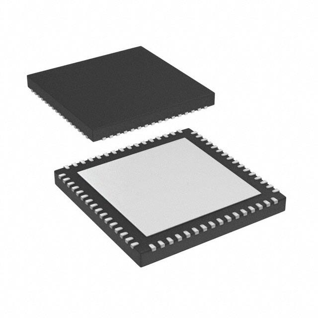


 工商网监
湘ICP备2023018690号
工商网监
湘ICP备2023018690号
