LMK02002
www.ti.com
SNAS418 – AUGUST 2007
LMK02002 Precision Clock Conditioner with Integrated PLL
Check for Samples: LMK02002
FEATURES
DESCRIPTION
•
•
The LMK02002 precision clock conditioner combines
the functions of jitter cleaning/reconditioning,
multiplication, and distribution of a reference clock.
The device integrates a high performance Integer-N
Phase Locked Loop (PLL), and four LVPECL clock
output distribution blocks.
1
2
•
•
•
•
•
•
20 fs Additive Jitter
Integrated Integer-N PLL with Outstanding
Normalized Phase Noise Contribution of -224
dBc/Hz
Clock Output Frequency Range of 1 to 800
MHz
4 LVPECL Clock Outputs
Dedicated Divider and Delay Blocks on Each
Clock Output
Pin Compatible Family of Clocking Devices
3.15 to 3.45 V Operation
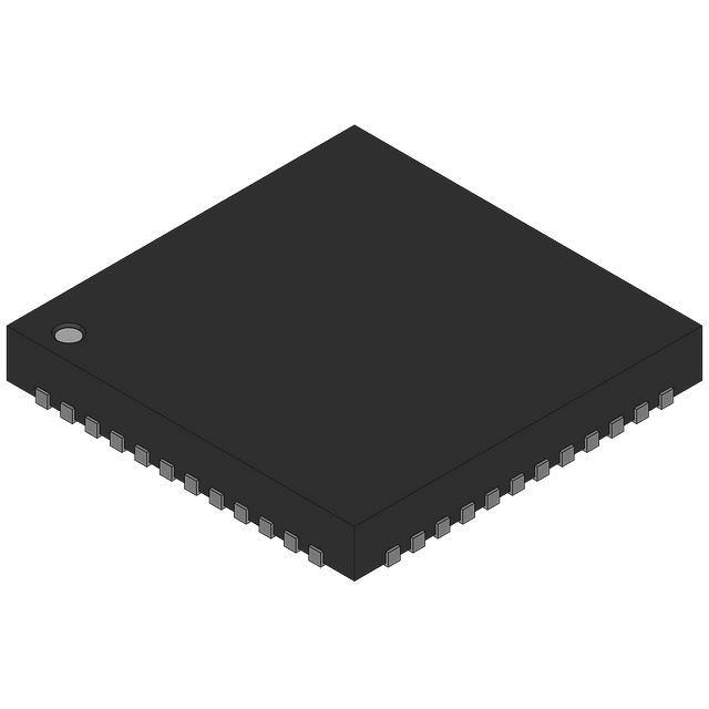
Package: 48 Pin WQFN (7.0 x 7.0 x 0.8 mm)
TARGET APPLICATIONS
•
•
•
•
•
•
Each
clock
distribution
block
includes
a
programmable divider, a phase synchronization
circuit, a programmable delay, a clock output mux,
and an LVPECL output buffer. This allows multiple
integer-related and phase-adjusted copies of the
reference to be distributed to eight system
components.
The clock conditioner comes in a 48-pin WQFN
package and is footprint compatible with other
clocking devices in the same family.
Data Converter Clocking
Networking, SONET/SDH, DSLAM
Wireless Infrastructure
Medical
Test and Measurement
Military / Aerospace
Functional Block Diagram
OSCin
OSCin*
R Divider
Phase
Detector
Charge
Pump
CPout
N Divider
Fin
Fin*
Distribution Path
Divider
DATA
Mux
CLKout0
CLKout0*
Mux
CLKout1
CLKout1*
Mux
CLKout2
CLKout2*
Mux
CLKout3
CLKout3*
Delay
CLK
PWire
Port
Control
Registers
LE
Divider
Delay
Divider
GOE
SYNC*
Device
Control
Delay
LD
Divider
Delay
Clock Buffers
1
2
Please be aware that an important notice concerning availability, standard warranty, and use in critical applications of
Texas Instruments semiconductor products and disclaimers thereto appears at the end of this data sheet.
All trademarks are the property of their respective owners.
PRODUCTION DATA information is current as of publication date.
Products conform to specifications per the terms of the Texas
Instruments standard warranty. Production processing does not
necessarily include testing of all parameters.
Copyright © 2007, Texas Instruments Incorporated
�LMK02002
SNAS418 – AUGUST 2007
www.ti.com
Connection Diagram
CLKout3*
CLKout3
Vcc14
CLKout2*
CLKout2
Vcc13
CLKout1*
CLKout1
Vcc12
CLKout0*
CLKout0
Vcc11
Figure 1. 48-Pin WQFN Package
48
47
46
45
44
43
42
41
40
39
38
37
GND
1
36
Bias
NC
2
35
Fin*
Vcc1
3
34
Fin
CLKuWire
4
33
Vcc10
DATAuWire
5
32
CPout
LEuWire
6
31
Vcc9
NC
7
30
Vcc8
Vcc2
8
29
OSCin*
LDObyp1
9
28
OSCin
LDObyp2
10
27
SYNC*
GOE
11
26
Vcc7
LD
12
25
GND
WQFN-48
Top Down View
17
18
19
20
NC
NC
Vcc4
NC
NC
Vcc5
NC
21
22
23
24
NC
16
NC
15
Vcc6
14
NC
13
Vcc3
DAP
Pin Descriptions
2
Pin #
Pin Name
I/O
1, 25
GND
-
Ground
Description
2, 7, 14, 15, 17, 18, 20,
21, 23, 24
NC
-
No Connection to these pins
3, 8, 13, 16, 19, 22, 26,
30, 31, 33, 37, 40, 43, 46
Vcc1, Vcc2, Vcc3, Vcc4, Vcc5, Vcc6, Vcc7, Vcc8,
Vcc9, Vcc10, Vcc11, Vcc12, Vcc13, Vcc14
-
Power Supply
4
CLKuWire
I
MICROWIRE Clock Input
5
DATAuWire
I
MICROWIRE Data Input
6
LEuWire
I
MICROWIRE Latch Enable Input
9, 10
LDObyp1, LDObyp2
-
LDO Bypass
11
GOE
I
Global Output Enable
12
LD
O
Lock Detect and Test Output
27
SYNC*
I
Global Clock Output Synchronization
28, 29
OSCin, OSCin*
I
Oscillator Clock Input; Must be AC coupled
32
CPout
O
Charge Pump Output
34, 35
Fin, Fin*
I
Frequency Input; Must be AC coupled
36
Bias
I
Bias Bypass
38, 39
CLKout0, CLKout0*
O
LVPECL Clock Output 0
41, 42
CLKout1, CLKout1*
O
LVPECL Clock Output 1
Submit Documentation Feedback
Copyright © 2007, Texas Instruments Incorporated
Product Folder Links: LMK02002
�LMK02002
www.ti.com
SNAS418 – AUGUST 2007
Pin Descriptions (continued)
Pin #
Pin Name
I/O
44, 45
CLKout2, CLKout2*
O
LVPECL Clock Output 2
Description
47, 48
CLKout3, CLKout3*
O
LVPECL Clock Output 3
DAP
DAP
-
Die Attach Pad is Ground
These devices have limited built-in ESD protection. The leads should be shorted together or the device placed in conductive foam
during storage or handling to prevent electrostatic damage to the MOS gates.
Absolute Maximum Ratings
(1) (2) (3)
Symbol
Ratings
Units
Power Supply Voltage
Parameter
VCC
-0.3 to 3.6
V
Input Voltage
VIN
-0.3 to (VCC + 0.3)
V
Storage Temperature Range
TSTG
-65 to 150
°C
Lead Temperature (solder 4 s)
TL
+260
°C
Junction Temperature
TJ
125
°C
(1)
(2)
(3)
"Absolute Maximum Ratings" indicate limits beyond which damage to the device may occur, including inoperability and degradation of
device reliability and/or performance. Functional operation of the device and/or non-degradation at the Absolute Maximum Ratings or
other conditions beyond those indicated in the Recommended Operating Conditions is not implied. The Recommended Operating
Conditions indicate conditions at which the device is functional and the device should not be operated beyond such conditions.
This device is a high performance integrated circuit with ESD handling precautions. Handling of this device should only be done at ESD
protected work stations. The device is rated to a HBM-ESD of > 2 kV, a MM-ESD of > 200 V, and a CDM-ESD of > 1.2 kV.
If Military/Aerospace specified devices are required, please contact the TI Sales Office/ Distributors for availability and specifications.
Recommended Operating Conditions
Symbol
Min
Typ
Max
Units
Ambient Temperature
Parameter
TA
-40
25
85
°C
Power Supply Voltage
VCC
3.15
3.3
3.45
V
Package Thermal Resistance
Package
48-Lead WQFN
(1)
(1)
θJA
θJ-PAD (Thermal Pad)
27.4° C/W
5.8° C/W
Specification assumes 16 thermal vias connect the die attach pad to the embedded copper plane on the 4-layer JEDEC board. These
vias play a key role in improving the thermal performance of the WQFN. It is recommended that the maximum number of vias be used in
the board layout.
Submit Documentation Feedback
Copyright © 2007, Texas Instruments Incorporated
Product Folder Links: LMK02002
3
�LMK02002
SNAS418 – AUGUST 2007
www.ti.com
Electrical Characteristics
(1)
(3.15 V ≤ Vcc ≤ 3.45 V, -40 °C ≤ TA ≤ 85 °C, Differential Inputs/Outputs; except as specified. Typical values represent most
likely parametric norms at Vcc = 3.3 V, TA = 25 °C, and at the Recommended Operation Conditions at the time of product
characterization and are not specified).
Symbol
Parameter
Conditions
Min
Typ
Max
Units
Current Consumption
ICC
Power Supply Current
ICCPD
(2)
Power Down Current
Entire device; CLKout0 & CLKout3
enabled in Bypass Mode
159
Entire device; All Outputs Off (no
emitter resistors placed)
70
POWERDOWN = 1
1
mA
mA
Reference Oscillator
Reference Oscillator Input Frequency
fOSCin square
Range for Square Wave
VOSCinsquare
Square Wave Input Voltage for OSCin and
OSCin*
fFin
Frequency Input Frequency Range
1
200
MHz
0.2
1.6
Vpp
1
800
MHz
AC coupled; Differential (VOD)
Frequency Input
SLEWFin
Frequency Input Slew Rate
DUTYFin
Frequency Input Duty Cycle
PFin
Input Power Range for Fin or Fin*
fCOMP
Phase Detector Frequency
See
(3) (4)
0.5
AC coupled
V/ns
40
60
%
-13
8
dBm
40
MHz
PLL
VCPout = Vcc/2, PLL_CP_GAIN = 1x
ISRCECPout
ISINKCPout
Charge Pump Source Current
Charge Pump Sink Current
100
VCPout = Vcc/2, PLL_CP_GAIN = 4x
400
VCPout = Vcc/2, PLL_CP_GAIN = 16x
1600
VCPout = Vcc/2, PLL_CP_GAIN = 32x
3200
VCPout = Vcc/2, PLL_CP_GAIN = 1x
-100
VCPout = Vcc/2, PLL_CP_GAIN = 4x
-400
VCPout = Vcc/2, PLL_CP_GAIN = 16x
-1600
VCPout = Vcc/2, PLL_CP_GAIN = 32x
-3200
µA
μA
ICPoutTRI
Charge Pump TRI-STATE Current
0.5 V < VCPout < Vcc - 0.5 V
2
ICPout%MIS
Magnitude of Charge Pump
Sink vs. Source Current Mismatch
VCPout = Vcc / 2
TA = 25°C
3
%
ICPoutVTUNE
Magnitude of Charge Pump
Current vs. Charge Pump Voltage Variation
0.5 V < VCPout < Vcc - 0.5 V
TA = 25°C
4
%
ICPoutTEMP
Magnitude of Charge Pump Current vs.
Temperature Variation
4
%
PN10kHz
PLL 1/f Noise at 10 kHz Offset (5)
Normalized to 1 GHz Output Frequency
(1)
(2)
(3)
(4)
(5)
4
PLL_CP_GAIN = 1x
-117
PLL_CP_GAIN = 32x
-122
10
nA
dBc/Hz
The Electrical Characteristics tables list ensured specifications under the listed Recommended Operating Conditions except as
otherwise modified or specified by the Electrical Characteristics Conditions and/or Notes. Typical specifications are estimations only and
are not ensured.
See CURRENT CONSUMPTION / POWER DISSIPATION CALCULATIONS for more current consumption / power dissipation
calculation information.
For all frequencies the slew rate, SLEWFin, is measured between 20% and 80%.
Specification is ensured by characterization and is not tested in production.
A specification in modeling PLL in-band phase noise is the 1/f flicker noise, LPLL_flicker(f), which is dominant close to the carrier. Flicker
noise has a 10 dB/decade slope. PN10kHz is normalized to a 10 kHz offset and a 1 GHz carrier frequency. PN10kHz = LPLL_flicker(10
kHz) - 20log(Fout / 1 GHz), where LPLL_flicker(f) is the single side band phase noise of only the flicker noise's contribution to total noise,
L(f). To measure LPLL_flicker(f) it is important to be on the 10 dB/decade slope close to the carrier. A high phase detector frequency and a
clean crystal are important to isolating this noise source from the total phase noise, L(f). LPLL_flicker(f) can be masked by the reference
oscillator performance if a low power or noisy source is used. The total PLL inband phase noise performance is the sum of LPLL_flicker(f)
and LPLL_flat(f).
Submit Documentation Feedback
Copyright © 2007, Texas Instruments Incorporated
Product Folder Links: LMK02002
�LMK02002
www.ti.com
SNAS418 – AUGUST 2007
Electrical Characteristics (1) (continued)
(3.15 V ≤ Vcc ≤ 3.45 V, -40 °C ≤ TA ≤ 85 °C, Differential Inputs/Outputs; except as specified. Typical values represent most
likely parametric norms at Vcc = 3.3 V, TA = 25 °C, and at the Recommended Operation Conditions at the time of product
characterization and are not specified).
Symbol
PN1Hz
Parameter
Conditions
Normalized Phase Noise Contribution (6)
Clock Distribution Section
JitterADD
Additive RMS Jitter
(7)
(4)
tSKEW
CLKoutX to CLKoutY
VOH
Output High Voltage
VOL
Output Low Voltage
VOD
Differential Output Voltage
(7)
Min
Typ
PLL_CP_GAIN = 1x
-219
PLL_CP_GAIN = 32x
-224
Max
Units
dBc/Hz
- LVPECL Clock Outputs (CLKout0 to CLKout3)
RL = 100 Ω
Distribution Path =
800 MHz
Bandwidth =
12 kHz to 20 MHz
CLKoutX_MUX =
Bypass
20
CLKoutX_MUX =
Divided
CLKoutX_DIV =
4
75
Equal loading and identical clock
configuration
Termination = 50 Ω to Vcc - 2 V
fs
-30
Termination = 50 Ω to Vcc - 2 V
CLKoutX output frequency = 200 MHz
660
Digital LVTTL Interfaces
±3
30
ps
Vcc 0.98
V
Vcc 1.8
V
810
965
mV
Vcc
V
0.8
V
(8)
VIH
High-Level Input Voltage
VIL
Low-Level Input Voltage
IIH
High-Level Input Current
VIH = Vcc
-5.0
5.0
µA
IIL
Low-Level Input Current
VIL = 0
-40.0
5.0
µA
IOH = +500 µA
Vcc 0.4
VOH
High-Level Output Voltage
VOL
Low-Level Output Voltage
2.0
IOL = -500 µA
Digital MICROWIRE Interfaces
V
0.4
V
Vcc
V
(9)
VIH
High-Level Input Voltage
1.6
VIL
Low-Level Input Voltage
0.4
V
IIH
High-Level Input Current
VIH = Vcc
-5.0
5.0
µA
IIL
Low-Level Input Current
VIL = 0
-5.0
5.0
µA
tCS
Data to Clock Set Up Time
See Data Input Timing
25
ns
tCH
Data to Clock Hold Time
See Data Input Timing
8
ns
tCWH
Clock Pulse Width High
See Data Input Timing
25
ns
tCWL
Clock Pulse Width Low
See Data Input Timing
25
ns
tES
Clock to Enable Set Up Time
See Data Input Timing
25
ns
tCES
Enable to Clock Set Up Time
See Data Input Timing
25
ns
tEWH
Enable Pulse Width High
See Data Input Timing
25
ns
MICROWIRE Timing
(6)
(7)
(8)
(9)
A specification in modeling PLL in-band phase noise is the Normalized Phase Noise Contribution, LPLL_flat(f), of the PLL and is defined
as PN1Hz = LPLL_flat(f) – 20log(N) – 10log(fCOMP). LPLL_flat(f) is the single side band phase noise measured at an offset frequency, f, in a
1 Hz Bandwidth and fCOMP is the phase detector frequency of the synthesizer. LPLL_flat(f) contributes to the total noise, L(f). To measure
LPLL_flat(f) the offset frequency, f, must be chosen sufficiently smaller then the loop bandwidth of the PLL, and yet large enough to avoid
a substantial noise contribution from the reference and flicker noise. LPLL_flat(f) can be masked by the reference oscillator performance if
a low power or noisy source is used.
The Clock Distribution Section includes all parts of the device except the PLL section. Typical Additive Jitter specifications apply to the
clock distribution section only.
Applies to GOE, LD, and SYNC*.
Applies to CLKuWire, DATAuWire, and LEuWire.
Submit Documentation Feedback
Copyright © 2007, Texas Instruments Incorporated
Product Folder Links: LMK02002
5
�LMK02002
SNAS418 – AUGUST 2007
www.ti.com
Serial Data Timing Diagram
MSB
DATAuWire
D27
LSB
D26
D25
D24
D23
D0
A3
A2
A1
A0
CLKuWire
tCES
tCS
tCH
tCWH
tES
tCWL
LEuWire
tEWH
Data bits set on the DATAuWire signal are clocked into a shift register, MSB first, on each rising edge of the
CLKuWire signal. On the rising edge of the LEuWire signal, the data is sent from the shift register to the
addressed register determined by the LSB bits. After the programming is complete the CLKuWire, DATAuWire,
and LEuWire signals should be returned to a low state.
Charge Pump Current Specification Definitions
I1 = Charge Pump Sink Current at VCPout = Vcc - ΔV
I2 = Charge Pump Sink Current at VCPout = Vcc/2
I3 = Charge Pump Sink Current at VCPout = ΔV
I4 = Charge Pump Source Current at VCPout = Vcc - ΔV
I5 = Charge Pump Source Current at VCPout = Vcc/2
I6 = Charge Pump Source Current at VCPout = ΔV
ΔV = Voltage offset from the positive and negative supply rails. Defined to be 0.5 V for this device.
Charge Pump Output Current Magnitude Variation vs. Charge Pump Output Voltage
6
Submit Documentation Feedback
Copyright © 2007, Texas Instruments Incorporated
Product Folder Links: LMK02002
�LMK02002
www.ti.com
SNAS418 – AUGUST 2007
Charge Pump Current Specification Definitions (continued)
Charge Pump Sink Current vs. Charge Pump Output Source Current Mismatch
Charge Pump Output Current Magnitude Variation vs. Temperature
Functional Description
The LMK02002 precision clock conditioner combines the functions of jitter cleaning/reconditioning, multiplication,
and distribution of a reference clock. The device integrates a high performance Integer-N Phase Locked Loop
(PLL), and four LVPECL clock output distribution blocks.
Each clock distribution block includes a programmable divider, a phase synchronization circuit, a programmable
delay, a clock output mux, and an LVPECL output buffer. This allows multiple integer-related and phase-adjusted
copies of the reference to be distributed to eight system components.
The clock conditioner comes in a 48-pin WQFN package and is footprint compatible with other clocking devices
in the same family.
BIAS PIN
To properly use the device, bypass Bias (pin 36) with a low leakage 1 µF capacitor connected to Vcc. This is
important for low noise performance.
LDO BYPASS
To properly use the device, bypass LDObyp1 (pin 9) with a 10 µF capacitor and LDObyp2 (pin 10) with a 0.1 µF
capacitor.
OSCILLATOR INPUT PORT (OSCin, OSCin*)
The purpose of OSCin is to provide the PLL with a reference signal. The OSCin port must be AC coupled, refer
to the System Level Diagram in the Application Information section. The OSCin port may be driven single
endedly by AC grounding OSCin* with a 0.1 µF capacitor.
FREQUENCY INPUT PORT (Fin, Fin*)
The purpose of Fin is to provide the PLL with a feedback signal from an external oscillator. The Fin port may be
driven single endedly by AC grounding Fin*.
Submit Documentation Feedback
Copyright © 2007, Texas Instruments Incorporated
Product Folder Links: LMK02002
7
�LMK02002
SNAS418 – AUGUST 2007
www.ti.com
CLKout DELAYS
Each individual clock output includes a delay adjustment. Clock output delay registers (CLKoutX_DLY) support a
150 ps step size and range from 0 to 2250 ps of total delay.
LVPECL OUTPUTS
Each LVPECL output may be disabled individually by programming the CLKoutX_EN bits. All the outputs may be
disabled simultaneously by pulling the GOE pin low or programming EN_CLKout_Global to 0.
GLOBAL CLOCK OUTPUT SYNCHRONIZATION
The SYNC* pin synchronizes the clock outputs. When the SYNC* pin is held in a logic low state, the divided
outputs are also held in a logic low state. When the SYNC* pin goes high, the divided clock outputs are activated
and will transition to a high state simultaneously. Clocks in the bypassed state are not affected by SYNC* and
are always synchronized with the divided outputs.
The SYNC* pin must be held low for greater than one clock cycle of the Frequency Input port, also known as the
distribution path. Once this low event has been registered, the outputs will not reflect the low state for four more
cycles. Similarly once the SYNC* pin becomes high, the outputs will not simultaneously transition high until four
more distribution path clock cycles have passed. See the timing diagram below for further detail. In the timing
diagram below the clocks are programmed as CLKout0_MUX = Bypassed, CLKout1_MUX = Divided,
CLKout1_DIV = 2, CLKout2_MUX = Divided, and CLKout2_DIV = 4.
SYNC* Timing Diagram
Distribution
Path
SYNC*
CLKout0
CLKout1
CLKout2
The SYNC* pin provides an internal pull-up resistor as shown on the functional block diagram. If the SYNC* pin
is not terminated externally the clock outputs will operate normally. If the SYNC* function is not used, clock
output synchronization is not specified.
CLKout OUTPUT STATES
Each clock output may be individually enabled with the CLKoutX_EN bits. Each individual output enable control
bit is gated with the Global Output Enable input pin (GOE) and the Global Output Enable bit
(EN_CLKout_Global).
All clock outputs can be disabled simultaneously if the GOE pin is pulled low by an external signal or
EN_CLKout_Global is set to 0.
8
CLKoutX
_EN bit
EN_CLKout
_Global bit
GOE pin
Clock X Output State
1
1
Low
Low
Don't care
0
Don't care
Off
0
Don't care
Don't care
Off
1
1
High / No Connect
Enabled
Submit Documentation Feedback
Copyright © 2007, Texas Instruments Incorporated
Product Folder Links: LMK02002
�LMK02002
www.ti.com
SNAS418 – AUGUST 2007
When an LVPECL output is in the Off state, the outputs are at a voltage of approximately 1 volt.
GLOBAL OUTPUT ENABLE AND LOCK DETECT
The GOE pin provides an internal pull-up resistor. If it is not terminated externally, the clock output states are
determined by the Clock Output Enable bits (CLKoutX_EN) and the EN_CLKout_Global bit.
By programming the PLL_MUX register to Digital Lock Detect Active High (See PLL_MUX[3:0] -- Multiplexer
Control for LD Pin), the Lock Detect (LD) pin can be connected to the GOE pin in which case all outputs are set
low automatically if the synthesizer is not locked.
POWER ON RESET
When supply voltage to the device increases monotonically from ground to Vcc, the power on reset circuit sets
all registers to their default values, see RESET bit -- R0 only for more information on default register values.
Voltage should be applied to all Vcc pins simultaneously.
General Programming Information
The LMK02002 device is programmed using several 32-bit registers which control the device's operation. The
registers consist of a data field and an address field. The last 4 register bits, ADDR[3:0] form the address field.
The remaining 28 bits form the data field DATA[27:0].
During programming, LEuWire is low and serial data is clocked in on the rising edge of clock (MSB first). When
LEuWire goes high, data is transferred to the register bank selected by the address field. Only registers R0 to
R7, R11, R14, and R15 need to be programmed for proper device operation.
It is required to program register R14.
RECOMMENDED PROGRAMMING SEQUENCE
The recommended programming sequence involves programming R0 with the reset bit set (RESET = 1) to
ensure the device is in a default state. It is not necessary to program R0 again. Registers are programmed in
order with R15 being the last register programmed. An example programming sequence is shown below.
•
•
•
•
•
Program R0 with the reset bit set (RESET = 1). This ensures the device is in a default state.
Program R4 to R7 as necessary with desired clocks with appropriate enable, mux, divider, and delay settings.
Program R11 with DIV4 setting if necessary.
Program R14 with global clock output bit, power down setting, PLL mux setting, and PLL R divider. It is
required to program register R14.
– R14 must be programmed in accordance with the register map as shown in the register map (see
Table 1).
Program R15 with PLL charge pump gain, and PLL N divider.
Submit Documentation Feedback
Copyright © 2007, Texas Instruments Incorporated
Product Folder Links: LMK02002
9
�LMK02002
SNAS418 – AUGUST 2007
www.ti.com
Table 1. LMK02002 REGISTER MAP
Re
gist
er
31
R0
RE
SE
T
0
0
0
0
0
0
0
0
0
0
0
0
R4
0
0
0
0
0
0
0
0
0
0
0
0
0
CLKout0
_MUX
[1:0]
CL
Kou
t0_
EN
CLKout0_DIV
[7:0]
0
CLKout1
_MUX
[1:0]
CL
Kou
t1_
EN
0
CLKout2
_MUX
[1:0]
CLKout3
_MUX
[1:0]
30
29
28
27
26
25
24
23
22
21
20
19
18
17
16
15
14
13
12
11
10
9
8
7
6
5
4
3
2
1
0
A3
A2
A1
A0
0
0
0
0
CLKout0_DLY
[3:0]
0
1
0
0
CLKout1_DIV
[7:0]
CLKout1_DLY
[3:0]
0
1
0
1
CL
Kou
t2_
EN
CLKout2_DIV
[7:0]
CLKout2_DLY
[3:0]
0
1
1
0
CL
Kou
t3_
EN
CLKout3_DIV
[7:0]
CLKout3_DLY
[3:0]
0
1
1
1
Data [27:0]
R5
R6
0
0
0
0
0
0
0
0
0
0
0
0
0
0
0
0
0
0
0
0
0
0
0
0
R7
0
0
0
0
0
0
0
0
0
0
0
0
0
R11
0
0
0
0
0
0
0
0
1
0
0
0
0
1
0
EN
_CL
Kou
t_Gl
oba
l
0
0
0
R14
R15
10
0
0
PLL_
CP_
GAIN
[1:0]
PO TRI PLL
WE
_C
RD ST P_
OW AT PO
N
E
L
0
0
0
0
1
0
0
PLL_MUX
[3:0]
0
DIV
4
0
0
0
0
PLL_R
[11:0]
PLL_N
[17:0]
Submit Documentation Feedback
0
0
0
0
0
0
0
0
0
0
0
0
0
0
0
0
0
0
1
0
1
1
0
0
0
0
1
1
1
0
0
0
0
0
1
1
1
1
Copyright © 2007, Texas Instruments Incorporated
Product Folder Links: LMK02002
�LMK02002
www.ti.com
SNAS418 – AUGUST 2007
REGISTER R4 to R7
Registers R4 through R7 control the eight clock outputs. Register R4 controls CLKout0, Register R5 controls
CLKout1, and so on. There is one additional bit in register R0 called RESET. Aside from this, the functions of
these bits are identical. The X in CLKoutX_MUX, CLKoutX_DIV, CLKoutX_DLY, and CLKoutX_EN denote the
actual clock output which may be from 0 to 3.
RESET bit -- R0 only
This bit is only in register R0. The use of this bit is optional and it should be set to '0' if not used. Setting this bit
to a '1' forces all registers to their power on reset condition and therefore automatically clears this bit. If this bit is
set, all other R0 bits are ignored and R0 needs to be programmed again if used with its proper values and
RESET = 0.
Default
Bit Value
Bit Name
Bit State
Bit Description
Register
Bit
Location
R0
31
RESET
0
No reset, normal operation
Reset to power on defaults
CLKoutX_MUX
0
Bypassed
CLKoutX mux mode
CLKoutX_EN
0
Disabled
CLKoutX enable
CLKoutX_DIV
1
Divide by 2
CLKoutX clock divide
CLKoutX_DLY
0
0 ps
CLKoutX clock delay
DIV4
0
PDF ≤ 20 MHz
Phase Detector Frequency
EN_CLKout_Global
1
Normal - CLKouts normal
Global clock output enable
27
POWERDOWN
0
Normal - Device active
Device power down
26
PLL_CP_TRI
0
Normal - PLL active
TRI-STATE PLL charge pump
PLL_CP_POL
0
Negative Polarity CP
Polarity of charge pump
PLL_MUX
0
Disabled
Multiplexer control for LD pin
PLL_R
10
R divider = 10
PLL R divide value
19:8
PLL_CP_GAIN
0
100 uA
Charge pump current
31:30
N divider = 760
PLL N divide value
PLL_N
760
18:17
R4 to R7
16
15:8
7:4
R11
15
25
R14
24
23:20
R15
25:8
CLKoutX_MUX[1:0] -- Clock Output Multiplexers
These bits control the Clock Output Multiplexer for each clock output. Changing between the different modes
changes the blocks in the signal path and therefore incurs a delay relative to the bypass mode. The different
MUX modes and associated delays are listed below.
CLKoutX_MUX[1:0]
Mode
Added Delay Relative to Bypass Mode
0
Bypassed (default)
0 ps
1
Divided
100 ps
2
Delayed
400 ps
(In addition to the programmed delay)
3
Divided and Delayed
500 ps
(In addition to the programmed delay)
CLKoutX_DIV[7:0] -- Clock Output Dividers
These bits control the clock output divider value. In order for these dividers to be active, the respective
CLKoutX_MUX (See CLKoutX_MUX[1:0] -- Clock Output Multiplexers) bit must be set to either "Divided" or
"Divided and Delayed" mode. After all the dividers are programed, the SYNC* pin must be used to ensure that all
edges of the clock outputs are aligned (See GLOBAL CLOCK OUTPUT SYNCHRONIZATION). The Clock
Output Dividers follow the VCO Divider so the final clock divide for an output is VCO Divider × Clock Output
Divider. By adding the divider block to the output path a fixed delay of approximately 100 ps is incurred.
The actual Clock Output Divide value is twice the binary value programmed as listed in the table below.
Submit Documentation Feedback
Copyright © 2007, Texas Instruments Incorporated
Product Folder Links: LMK02002
11
�LMK02002
SNAS418 – AUGUST 2007
www.ti.com
CLKoutX_DIV[7:0]
Clock Output Divider value
0
0
0
0
0
0
0
0
Invalid
0
0
0
0
0
0
0
1
2 (default)
0
0
0
0
0
0
1
0
4
0
0
0
0
0
0
1
1
6
0
0
0
0
0
1
0
0
8
0
0
0
0
0
1
0
1
10
.
.
.
.
.
.
.
.
...
1
1
1
1
1
1
1
1
510
CLKoutX_DLY[3:0] -- Clock Output Delays
These bits control the delay stages for each clock output. In order for these delays to be active, the respective
CLKoutX_MUX (See CLKoutX_MUX[1:0] -- Clock Output Multiplexers) bit must be set to either "Delayed" or
"Divided and Delayed" mode. By adding the delay block to the output path a fixed delay of approximately 400 ps
is incurred in addition to the delay shown in the table below.
CLKoutX_DLY[3:0]
Delay (ps)
0
0 (default)
1
150
2
300
3
450
4
600
5
750
6
900
7
1050
8
1200
9
1350
10
1500
11
1650
12
1800
13
1950
14
2100
15
2250
CLKoutX_EN bit -- Clock Output Enables
These bits control whether an individual clock output is enabled or not. If the EN_CLKout_Global bit (See
EN_CLKout_Global bit -- Global Clock Output Enable) is set to zero or if GOE pin is held low, all CLKoutX_EN
bit states will be ignored and all clock outputs will be disabled. See CLKout OUTPUT STATES for more
information on CLKout states.
CLKoutX_EN bit
Conditions
CLKoutX State
0
EN_CLKout_Global bit = 1
GOE pin = High / No Connect 1
Disabled (default)
1
Enabled
REGISTER R11
This register only has one bit and only needs to be programmed in the case that the phase detector frequency is
greater than 20 MHz and digital lock detect is used. Otherwise, it is automatically defaulted to the correct values.
DIV4
This bit divides the frequency presented to the digital lock detect circuitry by 4. It is necessary to get a reliable
output from the digital lock detect output in the case of a phase detector frequency greater than 20 MHz.
12
Submit Documentation Feedback
Copyright © 2007, Texas Instruments Incorporated
Product Folder Links: LMK02002
�LMK02002
www.ti.com
SNAS418 – AUGUST 2007
DIV4
Digital Lock Detect Circuitry Mode
0
Not divided; Phase detector frequency ≤ 20 MHz (default)
1
Divided by 4; Phase detector frequency > 20 MHz
REGISTER R14
The LMK02002 requires register R14 to be programmed as shown in the register map (see Table 1).
PLL_R[11:0] -- R Divider Value
These bits program the PLL R Divider and are programmed in binary fashion.
PLL_R[11:0]
PLL R Divide Value
0
0
0
0
0
0
0
0
0
0
0
0
Invalid
0
0
0
0
0
0
0
0
0
0
0
1
1
0
0
0
0
0
0
0
0
0
0
1
0
2
.
.
.
.
.
.
.
.
.
.
.
.
...
0
0
0
0
0
0
0
0
1
0
1
0
10 (default)
.
.
.
.
.
.
.
.
.
.
.
.
...
1
1
1
1
1
1
1
1
1
1
1
1
4095
PLL_MUX[3:0] -- Multiplexer Control for LD Pin
These bits set the output mode of the LD pin. The table below lists several different modes.
PLL_MUX[3:0]
Output Type
LD Pin Function
0
Hi-Z
Disabled (default)
1
Push-Pull
Logic High
2
Push-Pull
Logic Low
3
Push-Pull
Digital Lock Detect (Active High)
4
Push-Pull
Digital Lock Detect (Active Low)
5
Push-Pull
Analog Lock Detect
6
Open Drain NMOS
Analog Lock Detect
7
Open Drain PMOS
Analog Lock Detect
8
Invalid
9
Push-Pull
N Divider Output/2 (50% Duty Cycle)
10
Invalid
11
Push-Pull
R Divider Output/2 (50% Duty Cycle)
12 to 15
Invalid
POWERDOWN bit -- Device Power Down
This bit can power down the device. Enabling this bit powers down the entire device and all blocks, regardless of
the state of any of the other bits or pins.
POWERDOWN bit
Mode
0
Normal Operation (default)
1
Entire Device Powered Down
EN_CLKout_Global bit -- Global Clock Output Enable
This bit overrides the individual CLKoutX_EN bits (See CLKoutX_EN bit -- Clock Output Enables). When this bit
is set to 0, all clock outputs are disabled, regardless of the state of any of the other bits or pins. See CLKout
OUTPUT STATES for more information on CLKout states.
Submit Documentation Feedback
Copyright © 2007, Texas Instruments Incorporated
Product Folder Links: LMK02002
13
�LMK02002
SNAS418 – AUGUST 2007
www.ti.com
EN_CLKout_Global bit
Clock Outputs
0
All Off
1
Normal Operation (default)
PLL_CP_TRI bit -- PLL Charge Pump TRI-STATE
This bit sets the PLL charge pump TRI-STATE.
PLL_CP_TRI
PLL Charge Pump
0
Normal operation (default)
1
TRI-STATE
PLL_CP_POL bit -- PLL Charge Pump Polarity
This bit sets the polarity of the charge pump to either negative or positive. A negative charge pump is used with a
VCO or VCXO which decreases frequency with increasing tuning voltage. A positive charge pump is used with a
VCO or VCXO which increases frequency with increasing tuning voltage.
PLL_CP_POL
PLL Charge Pump Polarity
0
Negative (default)
1
Positive
Register R15
PLL_N[17:0] -- PLL N Divider
These bits program the divide value for the PLL N Divider. The PLL N Divider follows the VCO Divider and
precedes the PLL phase detector. Since the VCO Divider is also in the feedback path from the VCO to the PLL
Phase Detector, the total N divide value, NTotal, is also influenced by the VCO Divider value. NTotal = PLL N
Divider × VCO Divider. The VCO frequency is calculated as, fVCO = fOSCin × PLL N Divider × VCO Divider / PLL R
Divider. Since the PLL N divider is a pure binary counter, there are no illegal divide values for PLL_N[17:0]
except for 0.
PLL_N[17:0]
PLL N Divider Value
0
0
0
0
0
0
0
0
0
0
0
0
0
0
0
0
0
0
0
0
0
0
0
0
0
0
0
0
0
0
0
0
0
0
0
1
Invalid
1
.
.
.
.
.
.
.
.
.
.
.
.
.
.
.
.
.
.
...
0
0
0
0
0
0
0
0
1
0
1
1
1
1
1
0
0
0
760 (default)
.
.
.
.
.
.
.
.
.
.
.
.
.
.
.
.
.
.
...
1
1
1
1
1
1
1
1
1
1
1
1
1
1
1
1
1
1
262143
PLL_CP_GAIN[1:0] -- PLL Charge Pump Gain
These bits set the charge pump gain of the PLL.
14
PLL_CP_GAIN[1:0]
Charge Pump Gain
0
1x (default)
1
4x
2
16x
3
32x
Submit Documentation Feedback
Copyright © 2007, Texas Instruments Incorporated
Product Folder Links: LMK02002
�LMK02002
www.ti.com
SNAS418 – AUGUST 2007
APPLICATION INFORMATION
SYSTEM LEVEL DIAGRAM
The following shows the LMK02002 in a typical application. In this setup the clock may be multiplied,
reconditioned, and redistributed.
Vcc
100Ö
1 PF
Bias
0.1 PF
Fin*
Fin
CPout
0.1 PF
0.1 PF
OSCin
100Ö
CLKout0
CLKout0*
OSCin*
CLKout1
CLKout1*
0.1 PF
CLKout2
LEuWire
CLKuWire
CLKout3
CLKout3*
DATAuWire
To Host
To System
CLKout2*
SYNC*
LMK02002
LD
(optional)
GOE
LDObyp1
LDObyp2
10 PF
0.1 PF
Figure 2. Typical Application
BIAS PIN
To properly use the device, bypass Bias (pin 36) with a low leakage 1 µF capacitor connected to Vcc. This is
important for low noise performance.
LDO BYPASS
To properly use the device, bypass LDObyp1 (pin 9) with a 10 µF capacitor and LDObyp2 (pin 10) with a 0.1 µF
capacitor.
CURRENT CONSUMPTION / POWER DISSIPATION CALCULATIONS
Due to the myriad of possible configurations the following table serves to provide enough information to allow the
user to calculate estimated current consumption of the LMK02002. Unless otherwise noted Vcc = 3.3 V, TA = 25
°C.
Submit Documentation Feedback
Copyright © 2007, Texas Instruments Incorporated
Product Folder Links: LMK02002
15
�LMK02002
SNAS418 – AUGUST 2007
www.ti.com
Table 2. Block Current Consumption
Current
Consumption at
3.3 V (mA)
Power
Dissipated in
device (mW)
Power
Dissipated in
LVPECL emitter
resistors (mW)
70
231
-
The low clock buffer is enabled anytime one of CLKout0
through CLKout3 are enabled
9
29.7
-
LVPECL output, bypass mode (includes 120 Ω emitter
resistors)
40
72
60
LVPECL output, disabled mode (includes 120 Ω emitter
resistors)
17.4
38.3
19.1
0
0
-
Divide enabled, divide = 2
5.3
17.5
-
Divide enabled, divide > 2
8.5
28.0
-
Delay circuitry per Delay enabled, delay < 8
output
Delay enabled, delay > 7
5.8
19.1
-
9.9
32.7
-
Entire device
159
404.7
120
Block
Condition
Entire device,
core current
All outputs off; No LVPECL emitter resistors connected
Clock buffers
(internal)
Output buffers
LVPECL output, disabled mode. No emitter resistors
placed; open outputs
Divide circuitry
per output
CLKout0 & CLKout3 enabled in bypass mode
From Table 2 the current consumption can be calculated in any configuration. For example, the current for the
entire device with two LVPECL (CLKout0 and CLKout3) outputs in bypass mode can be calculated by adding up
the following blocks: core current, clock buffers, and two LVPECL output buffer currents. There will also be two
LVPECL outputs drawing emitter current, but some of the power from the current draw is dissipated in the
external 120 Ω resistors which doesn't add to the power dissipation budget for the device. If delays or divides are
switched in, then the additional current for these stages needs to be added as well.
For power dissipated by the device, the total current entering the device is multiplied by the voltage at the device
minus the power dissipated in any emitter resistors connected to any of the LVPECL outputs. If no emitter
resistors are connected to the LVPECL outputs, this power will be 0 watts. For example, in the case of two
LVPECL (CLKout0 and CLKout3) operating at 3.3 volts, we calculate 3.3 V × (70 + 9 + 40 + 40) mA = 3.3 V ×
159 mA = 524.7 mW. Because the LVPECL outputs have emitter resistors hooked up and the power dissipated
by these resistors is 60 mW for each clock, the total device power dissipation is 524.7 mW - 120 mW = 404.7
mW.
When an LVPECL output is active, ~1.9 V is the average voltage on each output as calculated from the LVPECL
VOH & VOL typical specification. Therefore the power dissipated in each emitter resistor is approximately (1.9 V)2 /
120 Ω = 30 mW. When an LVPECL output is disabled, the emitter resistor voltage is ~1.07 V. Therefore the
power dissipated in each emitter resistor is approximately (1.07 V)2 / 120 Ω = 9.5 mW.
THERMAL MANAGEMENT
Power consumption of the LMK02002 can be high enough to require attention to thermal management. For
reliability and performance reasons the die temperature should be limited to a maximum of 125 °C. That is, as an
estimate, TA (ambient temperature) plus device power consumption times θJA should not exceed 125 °C.
The package of the device has an exposed pad that provides the primary heat removal path as well as excellent
electrical grounding to the printed circuit board. To maximize the removal of heat from the package a thermal
land pattern including multiple vias to a ground plane must be incorporated on the PCB within the footprint of the
package. The exposed pad must be soldered down to ensure adequate heat conduction out of the package. A
recommended land and via pattern is shown in Figure 3. More information on soldering WQFN packages can be
obtained at www.ti.com.
16
Submit Documentation Feedback
Copyright © 2007, Texas Instruments Incorporated
Product Folder Links: LMK02002
�LMK02002
www.ti.com
SNAS418 – AUGUST 2007
5.0 mm, min
0.33 mm, typ
1.2 mm, typ
Figure 3.
To minimize junction temperature it is recommended that a simple heat sink be built into the PCB (if the ground
plane layer is not exposed). This is done by including a copper area of about 2 square inches on the opposite
side of the PCB from the device. This copper area may be plated or solder coated to prevent corrosion but
should not have conformal coating (if possible), which could provide thermal insulation. The vias shown in
Figure 3 should connect these top and bottom copper layers and to the ground layer. These vias act as “heat
pipes” to carry the thermal energy away from the device side of the board to where it can be more effectively
dissipated.
Submit Documentation Feedback
Copyright © 2007, Texas Instruments Incorporated
Product Folder Links: LMK02002
17
�PACKAGE OPTION ADDENDUM
www.ti.com
10-Dec-2020
PACKAGING INFORMATION
Orderable Device
Status
(1)
Package Type Package Pins Package
Drawing
Qty
Eco Plan
(2)
Lead finish/
Ball material
MSL Peak Temp
Op Temp (°C)
Device Marking
(3)
(4/5)
(6)
LMK02002ISQ/NOPB
ACTIVE
WQFN
RHS
48
250
RoHS & Green
SN
Level-3-260C-168 HR
-40 to 85
K02002 I
LMK02002ISQX/NOPB
ACTIVE
WQFN
RHS
48
2500
RoHS & Green
SN
Level-3-260C-168 HR
-40 to 85
K02002 I
(1)
The marketing status values are defined as follows:
ACTIVE: Product device recommended for new designs.
LIFEBUY: TI has announced that the device will be discontinued, and a lifetime-buy period is in effect.
NRND: Not recommended for new designs. Device is in production to support existing customers, but TI does not recommend using this part in a new design.
PREVIEW: Device has been announced but is not in production. Samples may or may not be available.
OBSOLETE: TI has discontinued the production of the device.
(2)
RoHS: TI defines "RoHS" to mean semiconductor products that are compliant with the current EU RoHS requirements for all 10 RoHS substances, including the requirement that RoHS substance
do not exceed 0.1% by weight in homogeneous materials. Where designed to be soldered at high temperatures, "RoHS" products are suitable for use in specified lead-free processes. TI may
reference these types of products as "Pb-Free".
RoHS Exempt: TI defines "RoHS Exempt" to mean products that contain lead but are compliant with EU RoHS pursuant to a specific EU RoHS exemption.
Green: TI defines "Green" to mean the content of Chlorine (Cl) and Bromine (Br) based flame retardants meet JS709B low halogen requirements of


 工商网监
湘ICP备2023018690号
工商网监
湘ICP备2023018690号

