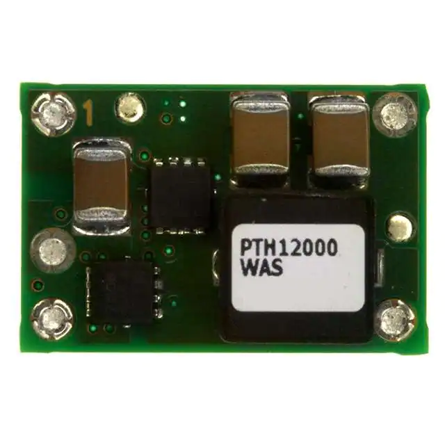
PTH12000W/L — 12-V Input
6-A, 12-V Input Non-Isolated
Wide-Output Adjust Power Module
SLTS202E– MAY 2003 – REVISED NOVENBER 2007
Features
NOMINAL SIZE =
0.75 in x 0.5 in
(19,05 mm x 12,7 mm)
• Up to 6-A Output Current
• 12-V Input Voltage
• Wide-Output Voltage Adjust
(1.2 V to 5.5 V)/(0.8 V to 1.8 V)
• 230 W/in³ Power Density
• Efficiencies up to 92 %
• Pre-Bias Startup
• On/Off Inhibit
• Under-Voltage Lockout
• Output Over-Current Protection
(Non-Latching, Auto-Reset)
• Operating Temp: –40 to +85 °C
• Surface Mount Package
• Safety Agency Approvals:
UL/cUL 60950, EN60950
VDE
Description
Pin Configuration
The PTH12000 series of non-isolated
power modules are small in size and high
on performance. Using double-sided surface mount construction and synchronous
rectification technology, these regulators
deliver up to 6 A of output current while
occupying a PCB area of about half the
size of a standard postage stamp. They
are an ideal choice for applications where
space, performance and cost are important design constraints.
The series operates from an input voltage of 12 V to provide step-down power
conversion to a wide range of output voltages. W-suffix devices are adjustable from
1.2 V to 5.5 V, and L-suffix devices are
adjustable from 0.8 V to 1.8 V. The out-
put voltage is set within the adjustment
range using a single external resistor.
Operating features include an on/off
inhibit, output voltage adjust (trim), and
the ability to start up into an existing
output voltage or prebias. A non-latching
over-current trip provides protection
against load faults.
Target applications include telecom,
industrial, and general purpose circuits,
including low-power dual-voltage systems
that use a DSP, microprocessor, or ASIC.
Package options include both throughhole and surface mount configurations.
Pin
1
2
3
4
5
Function
GND
Vin
Inhibit *
Vo Adjust
Vout
* Denotes negative logic:
Open
= Output On
Ground = Output Off
Standard Application
Rset = Required to set the output voltage higher than
the lowest value (see spec. table for values).
C1 = Required 100 μF capacitor
C2 = Optional 100 μF capacitor
C3 = Optional 10 μF ceramic capacitor
1
2
Inhibit
PTH12000x
(Top View)
4
+
C IN
100 µF
(Required)
3
GND
For technical support and further information visit http://power.ti.com
V OUT
5
C OUT
100 µF
(Optional)
+
V IN
R SET, 1%
(Required)
GND
�PTH12000W/L — 12-V Input
6-A, 12-V Input Non-Isolated
Wide-Output Adjust Power Module
SLTS202E– MAY 2003 – REVISED NOVENBER 2007
Ordering Information
Output Voltage (PTH12000rxx)
Package Options (PTH12000xrr) (1)
Code
W
L
Code
Voltage
1.2 V – 5.5 V
0.8 V – 1.8 V
(Adjust)
(Adjust)
AH
AS
Description
Horiz. T/H
SMD, Standard (3)
Pkg Ref.
(2)
(EUS)
(EUT)
Notes: (1) Add “T” to end of part number for tape and reel on SMD packages only.
(2) Reference the applicable package reference drawing for the dimensions and PC board layout
(3) “Standard” option specifies 63/37, Sn/Pb pin solder material.
Pin Descriptions
Vin: The positive input voltage power node to the module, which is referenced to common GND.
Vout: The regulated positive power output with respect
to the GND node.
GND: This is the common ground connection for the
‘Vin’ and ‘Vout’ power connections. It is also the 0 VDC
reference for the ‘Inhibit’ and ‘Vo Adjust’ control inputs.
Inhibit: The Inhibit pin is an open-collector/drain negative
logic input that is referenced to GND. Applying a lowlevel ground signal to this input disables the module’s
output and turns off the output voltage. When the Inhibit
control is active, the input current drawn by the regulator
is significantly reduced. If the Inhibit pin is left opencircuit, the module will produce an output whenever a
valid input source is applied.
Environmental & Absolute Maximum Ratings
Characteristics
Symbols
Operating Temperature Range
Solder Reflow Temperature(AS)
Solder Reflow Temperature(AZ)
Wave SolderTemperature(AH/AD)
Storage Temperature
Mechanical Shock
Ta
Treflow
Treflow
TWave
Ts
Mechanical Vibration
Weight
Flammability
—
—
Vo Adjust: A 1-% resistor must be connected between this
pin and GND (pin 1) to set the output voltage of the
module higher than its lowest value. The temperature
stability of the resistor should be 100 ppm/°C (or better).
The set-point range is 1.2 V to 5.5 V for W-suffix devices,
and 0.8 V to 1.8 V for L-suffix devices. The resistor value
required for a given output voltage may be calculated
using a formula. If left open circuit, the output voltage
will default to its lowest value. For further information
on output voltage adjustment consult the related application note.
The specification tables also give the preferred resistor
values for a number of standard output voltages.
(Voltages are with respect to GND)
Conditions
Over Vin Range
Surface temperature of module body or pins
Surface temperature of module body or pins
Surface temperature of module body or pins(5 seconds)
—
Per Mil-STD-883D, Method 2002.3
1 msec, ½ sine, mounted
Mil-STD-883D, Method 2007.2
20-2000 Hz
Min
Typ
Max
Units
–40 (i)
—
–55
—
+85
235 (ii)
260 (ii)
260 (ii)
+125
°C
°C
°C
°C
°C
—
500
—
G
—
15
—
G
—
2
—
grams
Meets UL 94V-O
Notes: (i) For operation below 0 °C the external capacitors must have stable characteristics. Use either a low ESR tantalum, Oscon, or ceramic capacitor.
(ii) During soldering of package version do not elevate peak temperature of the module, pins or internal components above the stated maximum.
For technical support and further information visit http://power.ti.com
�PTH12000W — 12-V Input
6-A, 12-V Input Non-Isolated
Wide-Output Adjust Power Module
Electrical Specifications
SLTS202E– MAY 2003 – REVISED NOVENBER 2007
Unless otherwise stated, T a =25 °C, Vin =12 V, V o =3.3 V, C 1 =100 μF, C2 =0 μF, C 3 =0 μF, and Io =Iomax
PTH12000W
Characteristics
Symbols
Conditions
Output Current
Io
Over ΔVadj range
Input Voltage Range
Set-Point Voltage Tolerance
Temperature Variation
Line Regulation
Load Regulation
Total Output Variation
Vin
Vo tol
ΔRegtemp
ΔRegline
ΔRegload
ΔRegtot
Over Io range
Ouput Voltage Adjust Range
Efficiency
ΔVadj
η
Vo Ripple (pk-pk)
Vr
Transient Response
Over-Current Threshold
Under-Voltage Lockout
ttr
ΔVtr
Io trip
UVLO
Inhibit Control (pin 3)
Input High Voltage
Input Low Voltage
Input Low Current
VIH
VIL
IIL
Standby Input Current
Switching Frequency
External Input Capacitance
External Output Capacitance
Iin standby
ƒs
Cin
Cout
Reliability
MTBF
Ta =60 °C, 200 LFM
Ta =25 °C, natural convection
–40 °C 2400 mA
8×12
8×10.5
7.3×5.7
1
1
1
≤4
≤4
≤4
20SVP100M
20SP120M
10TPE220ML
10 V
10 V
25 V
100 μF
220 μF
68 μF
0.100 Ω
0.100 Ω
0.095 Ω
>1090 mA
>1414 mA
>1451 mA
7.3L
×4.3W
×4.1H
N/R [2]
N/R [2]
2
≤5
≤5
≤5
TPSD107M010R0100
TPSV227M010R0100
TPSV686M025R0095
10 V
10 V
100 μF
100 μF
0.080 Ω
0.100 Ω
1200 mA
>1100 mA
7.3L×5.7W
×4.0H
N/R [2]
N/R [2]
≤5
≤5
T520D107M010AS
T495X107M010AS
10 V
25 V
16 V
150 μF
68 μF
100 μF
0.090 Ω
0.095 Ω
0.070 Ω
1100 mA
1600 mA
2890 mA
7.3L×6.0W
×4.1H
10×10.5
N/R [2]
2
1
≤5
≤5
≤5
594D157X0010C2T
594D686X0025R2T
94SP107X0016FBP
Kemet, Ceramic X5R (SMD)
16 V
6.3 V
10 μF
47 μF
0.002 Ω
0.002 Ω
—
1 [3]
N/R [2]
C1210C106M4PAC
≤5
≤5 [1] C1210C476K9PAC (Vo ≤5.1V)
Murata, Ceramic X5R (SMD)
6.3 V
6.3 V
16 V
16 V
100 μF
47 μF
22 μF
10 μF
0.002 Ω
—
1210 case
3225 mm
N/R [2]
N/R [2]
1 [3]
1 [3]
≤3 [1]
≤5 [1]
≤5
≤5
GRM32ER60J107M (Vo ≤5.1V)
GRM32ER60J476M (Vo ≤5.1V)
GRM32ER61C226K
GRM32DR61C106K
TDK, Ceramic X5R (SMD)
6.3 V
6.3 V
16 V
16 V
100 μF
47 μF
22 μF
10 μF
0.002 Ω
—
1210 case
3225 mm
N/R [2]
N/R [2]
1 [3]
1 [3]
≤3 [1]
≤5 [1]
≤5
≤5
C3225X5R0J107MT (Vo ≤5.1V)
C3225X5R0J476MT (Vo ≤5.1V)
C3225X5R1C226MT
C3225X5R1C106MT
AVX, Tantalum TPS (SMD)
Kemet
T520, Poy-Tant (SMD)
T495, Tantalum (SMD)
Vishay-Sprague
594D, Tantalum (SMD)
94SP, Organic (Radial)
Vendor Number
1210 case
3225 mm
EEUFC1E331
EEUFC1V181
EEVFK1E471P
PXA16VC151MJ80TP
20FP120MG
20FS100M
LXZ35VB221M10X12LL
UHD1E221MPR
UPM1V221MHH6
EEFWA1C101P
≤5
≤1 [1] EEFSE0J181R (Vo ≤5.1V)
[1] The voltage rating of this capacitor only allows it to be used for output voltages that are equal to or less than 5.1 V
[2] N/R –Not recommended. The capacitor voltage rating does not meet the minimum derated operating limits.
[3] A ceramic capacitor may be used to complement electrolytic types at the input to further reduce high-frequency ripple current.
For technical support and further information visit http://power.ti.com
�Application Notes
PTH12000 Series
Adjusting the Output Voltage of the PTH12000x
Wide-Output Adjust Power Modules
The Vo Adjust control (pin 4) sets the output voltage of
the PTH12000 product. The adjustment range is from
1.2 V to 5.5 V for the W-suffix modules, and 0.8 V to
1.8 V for L-suffix modules. The adjustment method
requires the addition of a single external resistor, R set,
that must be connected directly between the Vo Adjust
and GND pins 1. Table 2-1 gives the preferred value of the
external resistor for a number of standard voltages, along
with the actual output voltage that this resistance value
provides. Figure 2-1 shows the placement of the required
resistor.
Figure 2-1; Vo Adjust Resistor Placement
Table 2-1; Preferred Values of Rset for Standard Output Voltages
Inhibit
5.009 V
3.294 V
2.503 V
2.010 V
1.801 V
1.506 V
1.200 V
N/A
N/A
N/A
N/A
Rset
N/A
N/A
N/A
N/A
130 Ω
3.57 kΩ
12.1 kΩ
18.7 kΩ
32.4 kΩ
71.5 kΩ
Open
Vout (Actual)
N/A
N/A
N/A
N/A
1.800 V
1.499 V
1.201 V
1.101 V
0.999 V
0.901 V
0.800 V
For other output voltages the value of the required resistor
can either be calculated, or simply selected from the range
of values given in Table 2-3. The following formula may
be used for calculating the adjust resistor value. Select
the appropriate value for the parameters, Rs and Vmin,
from Table 2.2.
Rset
= 10 kΩ ·
0.8 V
Vout – Vmin
– Rs
Table 2.2; Adjust Formula Parameters
Pt. No.
V min
Vmax
Rs
VIN
PTH12000x
Inhibit
CIN
100µF
(Required)
3
VO
5
VOUT
GND
1
RSET, 1 %
COUT
100µF
(Optional)
PTH12000L
Vout (Actual)
280 Ω
2.0 kΩ
4.32 kΩ
8.06 kΩ
11.5 kΩ
24.3 kΩ
Open
N/A
N/A
N/A
N/A
2
+
5V
3.3 V
2.5 V
2V
1.8 V
1.5 V
1.2 V
1.1 V
1.0 V
0.9 V
0.8 V
Rset
VIN
+
PTH12000W
Vout (Req’d)
4
VO Adj
PTH12000W
PTH12000L
1.2 V
5.5 V
1.82 kΩ
0.8 V
1.8 V
7.87 kΩ
For technical support and further information visit http://power.ti.com
kΩ
GND
GND
Notes:
1. A 0.05-W rated resistor may be used. The tolerance
should be 1 %, with a temperature stability of 100 ppm/°C
or better. Place the resistor as close to the regulator as
possible. Connect the resistor directly between pins 4
and 1 using dedicated PCB traces.
2. Never connect capacitors from Vo Adjust to either GND or
Vout. Any capacitance added to the Vo Adjust pin will affect
the stability of the regulator.
�Application Notes continued
PTH12000 Series
Table 2-3; Output Voltage Set-Point Resistor Values
PTH12000W
VOUT
1.200
1.225
1.250
1.275
1.300
1.325
1.350
1.375
1.400
1.425
1.450
1.475
1.50
1.55
1.60
1.65
1.70
1.75
1.80
1.85
1.90
1.95
2.00
2.05
2.10
2.15
2.20
2.25
2.30
2.35
2.40
2.45
2.50
2.55
2.60
2.65
RSET
Open
318.0 kΩ
158.0 kΩ
105.0 kΩ
78.2 kΩ
62.2 kΩ
51.5 kΩ
43.9 kΩ
38.2 kΩ
33.7 kΩ
30.2 kΩ
27.3 kΩ
24.8 kΩ
21.0 kΩ
18.2 kΩ
16.0 kΩ
14.2 kΩ
12.7 kΩ
11.5 kΩ
10.5 kΩ
9.61 kΩ
8.85 kΩ
8.18 kΩ
7.59 kΩ
7.07 kΩ
6.60 kΩ
6.18 kΩ
5.80 kΩ
5.45 kΩ
5.14 kΩ
4.85 kΩ
4.58 kΩ
4.33 kΩ
4.11 kΩ
3.89 kΩ
3.70 kΩ
VOUT
2.70
2.75
2.80
2.85
2.90
2.95
3.00
3.05
3.10
3.15
3.20
3.25
3.30
3.35
3.40
3.50
3.60
3.70
3.80
3.90
4.00
4.10
4.20
4.30
4.40
4.50
4.60
4.70
4.80
4.90
5.00
5.10
5.20
5.30
5.40
5.50
PTH12000L
RSET
3.51 kΩ
3.34 kΩ
3.18 kΩ
3.03 kΩ
2.89 kΩ
2.75 kΩ
2.62 kΩ
2.50 kΩ
2.39 kΩ
2.28 kΩ
2.18 kΩ
2.08 kΩ
1.99 kΩ
1.90 kΩ
1.82 kΩ
1.66 kΩ
1.51 kΩ
1.38 kΩ
1.26 kΩ
1.14 kΩ
1.04 kΩ
939 Ω
847 Ω
761 Ω
680 Ω
604 Ω
533 Ω
466 Ω
402 Ω
342 Ω
285 Ω
231 Ω
180 Ω
131 Ω
85 Ω
41 Ω
VOUT
0.800
0.825
0.850
0.875
0.900
0.925
0.950
0.975
1.000
1.025
1.050
1.075
1.100
1.125
1.150
1.175
1.200
1.225
1.250
1.275
1.300
1.325
1.350
1.375
1.400
1.425
1.450
1.475
1.50
1.55
1.60
1.65
1.70
1.75
1.80
RSET
Open
312.0 kΩ
152.0 kΩ
98.8 kΩ
72.1 kΩ
56.1 kΩ
45.5 kΩ
37.8 kΩ
32.1 kΩ
27.7 kΩ
24.1 kΩ
21.2 kΩ
18.8 kΩ
16.7 kΩ
15.0 kΩ
13.5 kΩ
12.1 kΩ
11.0 kΩ
9.91 kΩ
8.97 kΩ
8.13 kΩ
7.37 kΩ
6.68 kΩ
6.04 kΩ
5.46 kΩ
4.93 kΩ
4.44 kΩ
3.98 kΩ
3.56 kΩ
2.8 kΩ
2.13 kΩ
1.54 kΩ
1.02 kΩ
551 Ω
130 Ω
For technical support and further information visit http://power.ti.com
�Application Notes
PTH12000 Series
Power-Up Characteristics
When configured per the standard application, the
PTH12000x power modules produce a regulated output voltage whenever of a valid input voltage is applied
from Vin (pin 2), with respect to GND (pin 1). During
the power-up period, internal soft-start circuitry slows the
rate that the output voltage rises. This reduces the in-rush
current drawn from the input source. The soft-start circuitry also introduces a short time delay (typically 12 ms)
into the power-up characteristic. The delay is from the
point that a valid input source is recognized, to the initial
rise of the output voltage. Figure 3-1 shows the powerup characteristic of the PTH12000W with the output
voltage set to 5-V. The waveforms were measured with a
2-A resistive load. The initial rise in input current when
the input voltage first starts to rise is the charge current
drawn by the input capacitors.
Figure 3-1
The power modules function normally when the Inhibit
pin is left open-circuit, providing a regulated output
whenever a valid source voltage is connected to Vin with
respect to GND.
Figure 3-2 shows the typical application of the inhibit
function. Note the discrete transistor (Q1). The Inhibit
pin has its own internal pull-up to V in potential. An
open-collector or open-drain device is recommended to
control this input.
Turning Q1 on applies a low voltage to the inhibit control
and disables the output of the module. If Q1 is then turned
off, the module will execute a soft-start power-up. A
regulated output voltage is produced within 25 msec.
Figure 3-3 shows the typical rise in both the output voltage and input current, following the turn-off of Q1. The
turn off of Q1 corresponds to the rise in the waveform,
Vinh. The waveforms were measured with a 5-V output
and 2-A resistive load.
Figure 3-2
Vin (5 V/Div)
VIN
2
PTH12000W
3
+
Iin (2 A/Div)
1
4
RSET
280
1%
C IN
100 µF
VOUT
5
+
Vo (5 V/Div)
Co1
100 µF
Q1
BSS138
1 =Inhibit
HORIZ SCALE: 5 ms/Div
GND
Over-Current Protection
For protectection against load faults, this series incorporates output over-current protection. Applying a load that
exceeds the module’s over-current threshold will cause
the regulated output to shut down. Following shut down
the module will periodically attempt to recover by initiating a soft-start power-up. This is often described as a
“hiccup” mode of operation, whereby the module continues in the cycle of successive shut down and power up
until the load fault is removed. During this period, the
average current flowing into the fault is significantly
reduced. Once the fault is removed, the module automatically recovers and returns to normal operation.
GND
Figure 3-3
Vo (2 V/Div)
Iin (1 A/Div)
Vinh (10 V/Div)
Output On/Off Inhibit
The inhibit control (pin 3) is used wherever there is a
requirement to turn off the regulator output while input
power is applied.
For technical support and further information visit http://power.ti.com
HORIZ SCALE: 5 ms/Div
L
O
A
D
�Application Notes
PTH12000 Series
Pre-Bias Startup Capability
The capability to start up into an output pre-bias condition is now a feature of the PTH12000 series of modules.
(Note: This is a feature enhancement for the the W-suffix
version; see note 1).
the Inhibit pin is held low, and whenver the output is
allowed to rise under soft-start control. Power up under
soft-start control occurs upon the removal of the ground
signal to the Inhibit pin (with input voltage applied), or
when input power is applied. To further ensure that the
regulator doesn’t sink output current, (even with a ground
signal applied to its Inhibit), the input voltage must always
be greater than the applied pre-bias source. This condition must exist throughout the power-up sequence 3.
A pre-bias startup condition occurs as a result of an external
voltage being present at the output of a power module prior
to its output becoming active. This often occurs in complex digital systems when current from another power
source is backfed through a dual-supply logic component,
such as an FPGA or ASIC. Another path might be via
clamp diodes, sometimes used as part of a dual-supply
power-up sequencing arrangement. A prebias can cause
problems with power modules that incorporate synchronous rectifiers. This is because under most operating
conditions, such modules can sink as well as source output
current. The PTH12000x series of modules incorporate
synchronous rectifiers, but will not sink current during
startup, or whenever the Inhibit pin is held low. Startup
includes an initial delay (approx. 8 - 15 ms), followed by
the rise of the output voltage under the control of the
module’s internal soft-start mechanism; see Figure 3-1.
The soft-start period is complete when the output begins
rising above the pre-bias voltage. Once it is complete the
module functions as normal, and will sink current if a
voltage higher than the nominal regulation value is applied
to its output.
Note: If a pre-bias condition is not present, the soft-start period
will be complete when the output voltage has risen to either
the set-point voltage.
Demonstration Circuit
The circuit shown in Figure 3-4 is a demonstrates the
pre-bias startup feature. Figure 3-5 shows the startup
waveforms. The initial rise in Vo 2 is the pre-bias voltage, which is passed from the VCCIO to the VCORE
voltage rail through the ASIC. Note that the output current from the PTH12000L module (Io2) is negligible
until its output voltage rises above the applied pre-bias.
Conditions for Pre-Bias Holdoff
In order for the module to allow an output pre-bias voltage
to exist (and not sink current), certain conditions must be
maintained. The module holds off a pre-bias voltage when
Figure 3–4; Application Circuit Demonstrating Pre-Bias Startup
10
9
VIN = 12 V
2
5
8
Up Dn
Track
Sense
PTH12020W
VIN
Inhibit
Adjust
GND
3
7
1
VO
2
R3
11k0
PTH12000L
VIN
VO
5
Vo2 = 1.8 V
+
8
Inh
VCC
7
2
1
3
3
SENSE
RESET
5
TL7702B
REF
RESET
6
CT
C5
0.1 µF
C6
0.68 µF
4
GND
Adj
1
Io2
4
R2
130
RESIN
330 µF
VCCIO
VCORE
+ C3
+ C4
330 µF
GND
R4
100k
330 µF
R1
2k
330 µF
Vo1 = 3.3 V
+C
2
4
+ C1
6
ASIC
R5
10k0
For technical support and further information visit http://power.ti.com
�Application Notes
PTH12000 Series
Figure 3–5; Pre-Bias Startup Waveforms
Vo 1 (1 V/Div)
Vo 2 (1 V/Div)
Hold-off
Period
Io 2 (2 A/Div)
HORIZ SCALE: 5 ms/Div
Notes
1. Output pre-bias holdoff has now been incorporated into
the W-suffix modules (PTH12000W), with a production
lot date code of “0423” or later.
2. To further ensure that the regulator’s output does not sink
current when power is first applied (even with a ground
signal applied to the Inhibit control pin), the input voltage
must always be greater than the applied pre-bias source.
This condition must exist throughout the power-up
sequence of the power system.
For technical support and further information visit http://power.ti.com
�PTH12000 Tape & Reel and Tray Specification
�PACKAGE OPTION ADDENDUM
www.ti.com
25-Dec-2021
PACKAGING INFORMATION
Orderable Device
Status
(1)
Package Type Package Pins Package
Drawing
Qty
Eco Plan
(2)
Lead finish/
Ball material
MSL Peak Temp
Op Temp (°C)
(3)
Device Marking
(4/5)
(6)
PTH12000LAH
ACTIVE
ThroughHole Module
EUS
5
56
RoHS (In
Work) & Green
(In Work)
SN
N / A for Pkg Type
-40 to 85
PTH12000LAZ
ACTIVE
Surface
Mount Module
EUT
5
49
RoHS (In
Work) & Green
(In Work)
SNAGCU
Level-3-260C-168 HR
-40 to 85
PTH12000LAZT
ACTIVE
Surface
Mount Module
EUT
5
250
RoHS (In
Work) & Green
(In Work)
SNAGCU
Level-3-260C-168 HR
-40 to 85
PTH12000WAD
ACTIVE
ThroughHole Module
EUS
5
56
RoHS Exempt
& Green
SN
N / A for Pkg Type
-40 to 85
PTH12000WAH
ACTIVE
ThroughHole Module
EUS
5
56
RoHS Exempt
& Green
SN
N / A for Pkg Type
-40 to 85
PTH12000WAS
ACTIVE
Surface
Mount Module
EUT
5
49
Non-RoHS
& Green
SNPB
Level-1-235C-UNLIM/
Level-3-260C-168HRS
-40 to 85
PTH12000WAZ
ACTIVE
Surface
Mount Module
EUT
5
49
RoHS (In
Work) & Green
SNAGCU
Level-3-260C-168 HR
-40 to 85
PTH12000WAZT
ACTIVE
Surface
Mount Module
EUT
5
250
RoHS (In
Work) & Green
SNAGCU
Level-3-260C-168 HR
-40 to 85
(1)
The marketing status values are defined as follows:
ACTIVE: Product device recommended for new designs.
LIFEBUY: TI has announced that the device will be discontinued, and a lifetime-buy period is in effect.
NRND: Not recommended for new designs. Device is in production to support existing customers, but TI does not recommend using this part in a new design.
PREVIEW: Device has been announced but is not in production. Samples may or may not be available.
OBSOLETE: TI has discontinued the production of the device.
(2)
RoHS: TI defines "RoHS" to mean semiconductor products that are compliant with the current EU RoHS requirements for all 10 RoHS substances, including the requirement that RoHS substance
do not exceed 0.1% by weight in homogeneous materials. Where designed to be soldered at high temperatures, "RoHS" products are suitable for use in specified lead-free processes. TI may
reference these types of products as "Pb-Free".
RoHS Exempt: TI defines "RoHS Exempt" to mean products that contain lead but are compliant with EU RoHS pursuant to a specific EU RoHS exemption.
Green: TI defines "Green" to mean the content of Chlorine (Cl) and Bromine (Br) based flame retardants meet JS709B low halogen requirements of


 工商网监
湘ICP备2023018690号
工商网监
湘ICP备2023018690号
