Product
Folder
Sample &
Buy
Technical
Documents
Support &
Community
Tools &
Software
TFP410
SLDS145C – OCTOBER 2001 – REVISED DECEMBER 2014
TFP410 TI PanelBus™ Digital Transmitter
1 Features
•
•
1
•
•
•
•
•
•
•
•
•
(1)
3 Description
(1)
Digital Visual Interface (DVI) Compliant
Supports Pixel Rates up to 165 MHz (Including
1080 p and WUXGA at 60 Hz)
Universal Graphics Controller Interface
– 12-Bit, Dual-Edge and 24-Bit, Single-Edge
Input Modes
– Adjustable 1.1 V to 1.8 V and Standard 3.3 V
CMOS Input Signal Levels
– Fully Differential and Single-Ended Input
Clocking Modes
– Standard Intel 12-Bit Digital Video Port
Compatible as on Intel™ 81x Chipsets
Enhanced PLL Noise Immunity
– On-Chip Regulators and Bypass Capacitors for
Reducing System Costs
Enhanced Jitter Performance
– No HSYNC Jitter Anomaly
– Negligible Data-Dependent Jitter
Programmable Using I2C Serial Interface
Monitor Detection Through Hot-Plug and Receiver
Detection
Single 3.3-V Supply Operation
64-Pin TQFP Using TI’s PowerPAD™ Package
TI’s Advanced 0.18-µm EPIC-5™ CMOS Process
Technology
Pin Compatible With SiI164 DVI Transmitter
The TFP410 device is a Texas Instruments
PanelBus™ flat-panel display product, part of a
comprehensive family of end-to-end DVI 1.0compliant solutions, targeted at the PC and consumer
electronics industry.
The TFP410 device provides a universal interface to
allow a glueless connection to most commonly
available graphics controllers. Some of the
advantages of this universal interface include
selectable bus widths, adjustable signal levels, and
differential and single-ended clocking. The adjustable
1.1-V to 1.8-V digital interface provides a low-EMI,
high-speed bus that connects seamlessly with 12-bit
or 24-bit interfaces. The DVI interface supports flatpanel display resolutions up to UXGA at 165 MHz in
24-bit true color pixel format.
The TFP410 device combines PanelBus circuit
innovation with TI’s advanced 0.18 μm EPIC-5 CMOS
process technology and TI’s ultralow ground
inductance PowerPAD package. The result is a
compact 64-pin TQFP package providing a reliable,
low-current, low-noise, high-speed digital interface
solution.
Device Information(1)
PART NUMBER
TFP410
PACKAGE
HTQFP (64)
BODY SIZE (NOM)
10.00 mm × 10.00 mm
(1) For all available packages, see the orderable addendum at
the end of the data sheet.
Typical HDMI Interface
The digital visual interface (DVI) specification is an industry
standard developed by the digital display working group
(DDWG) for high-speed digital connection to digital displays
and has been adopted by industry-leading PC and consumer
electronics manufacturers. The TFP410 is compliant to the
DVI Revision 1.0 specification.
2 Applications
•
•
•
•
(2)
DVD
Blu-ray
HD Projectors
DVI/HDMI Transmitter(2)
HDMI video-only
1
An IMPORTANT NOTICE at the end of this data sheet addresses availability, warranty, changes, use in safety-critical applications,
intellectual property matters and other important disclaimers. PRODUCTION DATA.
�TFP410
SLDS145C – OCTOBER 2001 – REVISED DECEMBER 2014
www.ti.com
Table of Contents
1
2
3
4
5
6
7
7.5 Programming........................................................... 17
7.6 Register Maps ........................................................ 18
Features ..................................................................
Applications ...........................................................
Description .............................................................
Revision History.....................................................
Pin Configuration and Functions .........................
Specifications.........................................................
1
1
1
2
3
6
6.1
6.2
6.3
6.4
6.5
6.6
6.7
6
6
6
6
7
7
9
10 Layout................................................................... 29
Detailed Description ............................................ 10
11 Device and Documentation Support ................. 34
7.1
7.2
7.3
7.4
Absolute Maximum Ratings ......................................
ESD Ratings ............................................................
Recommended Operating Conditions.......................
Thermal Information ..................................................
Electrical Characteristics...........................................
Timing Requirements ................................................
Typical Characteristics ..............................................
Overview .................................................................
Functional Block Diagram .......................................
Feature Description.................................................
Device Functional Modes........................................
10
11
11
12
8
Application and Implementation ........................ 25
8.1 Application Information............................................ 25
8.2 Typical Application ................................................. 25
9
Power Supply Recommendations...................... 28
9.1 DVDD ...................................................................... 28
9.2 TVDD ...................................................................... 28
9.3 PVDD ...................................................................... 28
10.1 Layout Guidelines ................................................. 29
10.2 Layout Example .................................................... 30
10.3 TI PowerPAD 64-Pin HTQFP Package................. 33
11.1 Trademarks ........................................................... 34
11.2 Electrostatic Discharge Caution ............................ 34
11.3 Glossary ................................................................ 34
12 Mechanical, Packaging, and Orderable
Information ........................................................... 34
4 Revision History
Changes from Revision B (May 2011) to Revision C
•
2
Page
Added ESD Ratings table, Thermal Information table, Typical Characteristics section, Feature Description section,
Device Functional Modes, Application and Implementation section, Power Supply Recommendations section,
Layout section, Device and Documentation Support section, and Mechanical, Packaging, and Orderable Information
section. .................................................................................................................................................................................. 1
Submit Documentation Feedback
Copyright © 2001–2014, Texas Instruments Incorporated
Product Folder Links: TFP410
�TFP410
www.ti.com
SLDS145C – OCTOBER 2001 – REVISED DECEMBER 2014
5 Pin Configuration and Functions
DVDD
RESERVED
DKEN
DATA22
DATA23
DATA21
DATA20
DATA18
DATA19
DATA17
DATA16
DATA15
DATA13
DATA14
DGND
DATA12
PAP Package
64 Pin HTQFP
Top View
48 47 46 45 44 43 42 41 40 39 38 37 36 35 34 33
NC
49
32
TGND
DATA11
50
31
TX2+
DATA10
51
30
TX2-
DATA9
52
29
TVDD
DATA8
53
28
TX1+
DATA7
54
27
TX1-
DATA6
55
26
TGND
TX0+
59
22
TVC+
DATA3
60
21
TXC-
DATA2
20
19
TGND
DATA1
61
62
DATA0
63
18
PVDD
DGND
64
17
PGND
8
9 10 11 12 13 14 15 16
TFADJ
DGND
7
BSEL/SCL
6
DSEL/SDA
5
ISEL/RST
4
DVDD
3
PD
2
MSEN/PO1
1
CTL1/A1/DK1
DATA4
EDGE/HTPLG
TVDD
CTL2/A2/DK2
23
VSYNC
58
CTL3/A3/DK3
TX0-
DATA5
VREF
24
HSYNC
25
57
DE
56
DVDD
IDCKIDCK+
Pin Functions
PIN
NAME
NO.
TYPE
DESCRIPTION
INPUT
The upper 12 bits of the 24-bit pixel bus
DATA[23:12]
36−47
DATA[11:0]
50−55,
58−63
I
In 24-bit, single-edge input mode (BSEL = high), this bus inputs the top half of the 24-bit pixel bus. In
12-bit, dual-edge input mode (BSEL = low), these bits are not used to input pixel data. In this mode,
the state of DATA[23:16] is input to the I2C register CFG. This allows 8 bits of user configuration data
to be read by the graphics controller through the I2C interface (see the Register Maps section).
Note: All unused data inputs should be tied to GND or VDD.
The lower 12 bits of the 24-bit pixel bus/12-bit pixel bus input
I
In 24-bit, single-edge input mode (BSEL = high), this bus inputs the bottom half of the 24-bit pixel
bus. In 12-bit, dual-edge input mode (BSEL = low), this bus inputs 1/2 a pixel (12 bits) at every latch
edge (both rising and falling) of the clock.
Submit Documentation Feedback
Copyright © 2001–2014, Texas Instruments Incorporated
Product Folder Links: TFP410
3
�TFP410
SLDS145C – OCTOBER 2001 – REVISED DECEMBER 2014
www.ti.com
Pin Functions (continued)
PIN
NAME
IDCK–
IDCK+
NO.
56
57
TYPE
DESCRIPTION
I
Differential clock input. The TFP410 supports both single-ended and fully differential clock input
modes. In the single-ended clock input mode, the IDCK+ input (pin 57) should be connected to the
single-ended clock source and the IDCK− input (pin 56) should be tied to GND. In the differential
clock input mode, the TFP410 uses the crossover point between the IDCK+ and IDCK– signals as
the timing reference for latching incoming data DATA[23:0], DE, HSYNC, and VSYNC. The
differential clock input mode is only available in the low signal swing mode.
DE
2
I
Data enable. As defined in DVI 1.0 specification, the DE signal allows the transmitter to encode pixel
data or control data on any given input clock cycle. During active video (DE = high), the transmitter
encodes pixel data, DATA[23:0]. During the blanking interval (DE = low), the transmitter encodes
HSYNC, VSYNC and CTL[3:1].
HSYNC
4
I
Horizontal sync input
VSYNC
5
I
Vertical sync input
The operation of these three multifunction inputs depends on the settings of the ISEL (pin 13) and
DKEN (pin 35) inputs. All three inputs support 3.3-V CMOS signal levels and contain weak pulldown
resistors so that if left unconnected they default to all low.
CTL3/A3/DK3
CTL2/A2/DK2
CTL1/A1/DK1
6
7
8
I
When the I2C bus is disabled (ISEL = low) and the de-skew mode is disabled (DKEN = low), these
three inputs become the control inputs, CTL[3:1], which can be used to send additional information
across the DVI link during the blanking interval (DE = low). The CTL3 input is reserved for HDCP
compliant DVI TXs (TFP510) and the CTL[2:1] inputs are reserved for future use.
When the I2C bus is disabled (ISEL = low) and the de-skew mode is enabled (DKEN = high), these
three inputs become the de-skew inputs DK[3:1], used to adjust the setup and hold times of the pixel
data inputs DATA[23:0], relative to the clock input IDCK±.
When the I2C bus is enabled (ISEL = high), these three inputs become the 3 LSBs of the I2C slave
address, A[3:1].
CONFIGURATION/PROGRAMMING
Monitor sense/programmable output 1. The operation of this pin depends on whether the I2C
interface is enabled or disabled. This pin has an open-drain output and is only 3.3-V tolerant. An
external 5-kΩ pullup resistor connected to VDD is required on this pin.
MSEN/PO1
11
O
When I2C is disabled (ISEL = low), a low level indicates a powered on receiver is detected at the
differential outputs. A high level indicates a powered on receiver is not detected. This function is only
valid in dc-coupled systems.
When I2C is enabled (ISEL = high), this output is programmable through the I2C interface (see the
I2C register descriptions section).
I2C interface select/I2C RESET (active low, asynchronous)
If ISEL is high, then the I2C interface is active. Default values for the I2C registers can be found in
the Register Maps section.
ISEL/RST
13
I
If ISEL is low, then I2C is disabled and the chip configuration is specified by the configuration pins
(BSEL, DSEL, EDGE, VREF) and state pins (PD, DKEN).
If ISEL is brought low and then back high, the I2C state machine is reset. The register values are
changed to their default values and are not preserved from before the reset.
Input bus select/I2C clock input. The operation of this pin depends on whether the I2C interface is
enabled or disabled. This pin is only 3.3-V tolerant.
BSEL/SCL
15
I
When I2C is disabled (ISEL = low), a high level selects 24-bit input, single-edge input mode. A low
level selects 12-bit input, dual-edge input mode.
When I2C is enabled (ISEL = high), this pin functions as the I2C clock input (see the Register Maps
section). In this configuration, this pin has an open-drain output that requires an external 5-kΩ pullup
resistor connected to VDD.
DSEL/I2C data. The operation of this pin depends on whether the I2C interface is enabled or
disabled. This pin is only 3.3-V tolerant.
DSEL/SDA
14
I/O
When I2C is disabled (ISEL = low), this pin is used with BSEL and VREF to select the single-ended or
differential input clock mode (see Table 1).
When I2C is enabled (ISEL = high), this pin functions as the I2C bidirectional data line. In this
configuration, this pin has an open-drain output that requires an external 5-kΩ pullup resistor
connected to VDD.
4
Submit Documentation Feedback
Copyright © 2001–2014, Texas Instruments Incorporated
Product Folder Links: TFP410
�TFP410
www.ti.com
SLDS145C – OCTOBER 2001 – REVISED DECEMBER 2014
Pin Functions (continued)
PIN
NAME
NO.
TYPE
DESCRIPTION
Edge select/hot plug input. The operation of this pin depends on whether the I2C interface is enabled
or disabled. This input is 3.3-V tolerant only.
EDGE/HTPLG
9
I
When I2C is disabled (ISEL = low), a high level selects the primary latch to occur on the rising edge
of the input clock IDCK+. A low level selects the primary latch to occur on the falling edge of the
input clock IDCK+. This is the case for both single-ended and differential input clock modes.
When I2C is enabled (ISEL = high), this pin is used to monitor the hot plug detect signal. When used
for hot-plug detection, this pin requires a series
1-kΩ resistor.
Data de-skew enable. The de-skew function can be enabled either through I2C or by this pin when
I2C is disabled. When de-skew is enabled, the input clock to data setup/hold time can be adjusted in
discrete trim increments. The amount of trim per increment is defined by t(STEP).
DKEN
35
I
When I2C is disabled (ISEL = low), a high level enables de-skew with the trim increment determined
by pins DK[3:1] (see the Data De-skew Feature section). A low level disables de-skew and the
default trim setting is used.
When I2C is enabled (ISEL = high), the value of DKEN and the trim increment are selected through
I2C. In this configuration, the DKEN pin should be tied to either GND or VDD to avoid a floating input.
Input reference voltage. Selects the swing range of the digital data inputs (DATA[23:0], DE, HSYNC,
VSYNC, and IDCK±).
VREF
3
I
For high-swing 3.3-V input signal levels, VREF should be tied to VDD.
For low-swing input signal levels, VREF should be set to half of the maximum input voltage level. See
Recommended Operating Conditions for the allowable range for VREF.
The desired VREF voltage level is typically derived using a simple voltage-divider circuit.
Power down (active low). In the powerdown state, only the digital I/O buffers and I2C interface remain
active.
PD
10
I
When I2C is disabled (ISEL = low), a high level selects the normal operating mode. A low level
selects the powerdown mode.
When I2C is enabled (ISEL = high), the power-down state is selected through I2C. In this
configuration, the PD pin should be tied to GND.
Note: The default register value for PD is low, so the device is in powerdown mode when I2C is first
enabled or after an I2C RESET.
RESERVED
RESERVED
34
I
This pin is reserved and must be tied to GND for normal operation.
DVI DIFFERENTIAL SIGNAL OUTPUT PINS
TX0+
TX0−
25
24
O
Channel 0 DVI differential output pair. TX0± transmits the 8-bit blue pixel data during active video
andHSYNC and VSYNC during the blanking interval.
TX1+
TX1−
28
27
O
Channel 1 DVI differential output pair. TX1± transmits the 8-bit green pixel data during active video
and CTL[1] during the blanking interval.
TX2+
TX2−
31
30
O
Channel 2 DVI differential output pair. TX2± transmits the 8-bit red pixel data during active video and
CTL[3:2] during the blanking interval.
TXC+
TXC−
22
21
O
DVI differential output clock.
TFADJ
19
I
Full-scale adjust. This pin controls the amplitude of the DVI output voltage swing, determined by the
value of the pullup resistor RTFADJ connected to TVDD.
POWER AND GROUND PINS
DVDD
1, 12, 33
Power
Digital power supply. Must be set to 3.3 V nominal.
PVDD
18
Power
PLL power supply. Must be set to 3.3 V nominal.
TVDD
23, 29
Power
Transmitter differential output driver power supply. Must be set to 3.3 V nominal.
DGND
16, 48,
64
Ground Digital ground
PGND
17
TGND
20, 26,
32
NC
49
Ground PLL ground
Ground Transmitter differential output driver ground
NC
No connection required. If connected, tie high.
Submit Documentation Feedback
Copyright © 2001–2014, Texas Instruments Incorporated
Product Folder Links: TFP410
5
�TFP410
SLDS145C – OCTOBER 2001 – REVISED DECEMBER 2014
www.ti.com
6 Specifications
6.1 Absolute Maximum Ratings
over operating free-air temperature range (unless otherwise noted) (1)
DVDD, PVDD,
TVDD
RT
MIN
MAX
Supply voltage range
–0.5
4
Input voltage, logic/analog signals
–0.5
External DVI single-ended termination resistance
(1)
V
4
V
0 to open circuit
Ω
300 to open circuit
Ω
Case temperature for 10 seconds
260
°C
JEDEC latch-up (EIA/JESD78)
100
mA
Storage temperature
260
°C
External TFADJ resistance, RTFADJ
Tstg
UNIT
Stresses beyond those listed under Absolute Maximum Ratings may cause permanent damage to the device. These are stress ratings
only, which do not imply functional operation of the device at these or any other conditions beyond those indicated under Recommended
Operating Conditions. Exposure to absolute-maximum-rated conditions for extended periods may affect device reliability.
6.2 ESD Ratings
VALUE
V(ESD)
(1)
Human body model (HBM), per
ANSI/ESDA/JEDEC JS-001 (1)
Electrostatic discharge
DVI pins
±4000
All other pins
±2000
UNIT
V
JEDEC document JEP155 states that 500-V HBM allows safe manufacturing with a standard ESD control process.
6.3 Recommended Operating Conditions
over operating free-air temperature range (unless otherwise noted)
VDD
Supply voltage (DVDD, PVDD, TVDD)
Low-swing mode
MIN
NOM
MAX
3.0
3.3
3.6
UNIT
V
0.55 VDDQ/2 (1)
0.9
V
DVDD
V
VREF
Input reference voltage
AVDD
DVI termination supply voltage (2)
DVI receiver
3.14
3.3
3.46
V
RT
DVI Single-ended termination resistance (3)
DVI receiver
45
50
55
Ω
505
510
515
Ω
0
25
70
°C
High-swing mode
R(TFADJ) TFADJ resistor for DVI-compliant V(SWING) range
TA
(1)
(2)
(3)
400 mV = V(SWING) = 600 mV
Operating free-air temperature range
VDDQ defines the maximum low-level input voltage, it is not an actual input voltage.
AVDD is the termination supply voltage of the DVI link.
RT is the single-ended termination resistance at the receiver end of the DVI link.
6.4 Thermal Information
TFP410
THERMAL METRIC
(1)
PAP
UNIT
64 PINS
RθJA
Junction-to-ambient thermal resistance
26.6
RθJC(top)
Junction-to-case (top) thermal resistance
14.1
RθJB
Junction-to-board thermal resistance
11.3
ψJT
Junction-to-top characterization parameter
0.4
ψJB
Junction-to-board characterization parameter
11.2
RθJC(bot)
Junction-to-case (bottom) thermal resistance
0.9
(1)
6
°C/W
For more information about traditional and new thermal metrics, see the IC Package Thermal Metrics application report (SPRA953).
Submit Documentation Feedback
Copyright © 2001–2014, Texas Instruments Incorporated
Product Folder Links: TFP410
�TFP410
www.ti.com
SLDS145C – OCTOBER 2001 – REVISED DECEMBER 2014
6.5 Electrical Characteristics
over recommended operating free-air temperature range (unless otherwise noted)
PARAMETER
TEST CONDITIONS
MIN
TYP
MAX
UNIT
DC SPECIFICATIONS
VREF = DVDD
0.7 VDD
VIH
High-level input voltage (CMOS input)
VIL
Low-level input voltage (CMOS input)
VOH
High-level digital output voltage (open-drain
output)
VDD = 3 V, IOH = 20 μA
VOL
Low-level digital output voltage (open-drain
output)
VDD = 3.6 V, IOL = 4 mA
0.4
V
IIH
High-level input current
VI = 3.6 V
±25
µA
IIL
Low-level input current
VI = 0
±25
µA
VH
DVI single-ended high-level output voltage
AVDD – 0.01
AVDD + 0.01
V
VL
DVI single-ended low-level output voltage
AVDD – 0.6
AVDD – 0.4
VSWING
DVI single-ended output swing voltage
400
600
VOFF
DVI single-ended standby/off output voltage
IPD
Power-down current (2)
IIDD
Normal power supply current
0.5 V ≤ V ≤ 0.95 V
V
VREF + 0.2
VREF = DVDD
0.3VDD
0.5 V ≤V ≤ 0.95 V
AVDD = 3.3 V ± 5%,
RT (1) = 50 Ω ± 10%,
RTFADJ = 510 Ω ± 1%
VREF – 0.2
2.4
V
V
AVDD – 0.01
Worst-case pattern (3)
V
mVP-P
AVDD + 0.01
V
200
500
µA
200
250
mA
AC SPECIFICATIONS
f(IDCK)
IDCK frequency
25
165
MHz
tr
DVI output rise time (20-80%) (4)
75
240
ps
tf
DVI output fall time (20-80%) (4)
75
240
ps
tsk(D)
DVI output intra-pair + to − differential skew
see Figure 4
tojit
DVI output clock jitter, max.
t(STEP)
De-skew trim increment
(1)
(2)
(3)
(4)
(5)
(6)
(5)
,
f(IDCK) = 165 MHz
50
ps
(6)
150
DKEN = 1
350
ps
ps
RT is the single-ended termination resistance at the receiver end of the DVI link
Assumes all inputs to the transmitter are not toggling.
Black and white checkerboard pattern, each checker is one pixel wide.
Rise and fall times are measured as the time between 20% and 80% of signal amplitude.
Measured differentially at the 50% crossing point using the IDCK+ input clock as a trigger.
Relative to input clock (IDCK).
6.6 Timing Requirements
MIN
NOM
MAX
t(pixel)
Pixel time period (1)
6.06
40
t(IDCK)
IDCK duty cycle
30%
70%
t(ijit)
IDCK clock jitter tolerance
tsk(CC)
DVI output inter-pair or channel-to-channel skew
tsu(IDF)
Data, DE, VSYNC, HSYNC setup time to IDCK+ falling edge, see
Figure 2
th(IDF)
Data, DE, VSYNC, HSYNC hold time to IDCK+ falling edge, see
Figure 2
tsu(IDR)
Data, DE, VSYNC, HSYNC setup time to IDCK+ rising edge, see
Figure 2
th(IDR)
Data, DE, VSYNC, HSYNC hold time to IDCK+ rising edge, see
Figure 2
tsu(ID)
Data, DE, VSYNC, HSYNC setup time to IDCK+ falling/rising
edge, see Figure 3
Dual edge(BSEL=0,
DSEL=1, DKEN=0)
th(ID)
Data, DE, VSYNC, HSYNC hold time to IDCK+ falling/rising edge,
see Figure 3
Dual edge (BSEL=0,
DSEL=1, DKEN=0)
(1)
(2)
2
(2)
, see Figure 2
f(IDCK) = 165 MHz
Single edge (BSEL=1, DSEL=0,
DKEN=0, EDGE=0)
Single edge (BSEL=1, DSEL=0,
DKEN=0, EDGE=1)
UNIT
ns
ns
1.2
ns
1.2
ns
1.3
ns
1.2
ns
1.3
ns
0.9
ns
1
ns
t(pixel) is the pixel time defined as the period of the TXC output clock. The period of IDCK is equal to t(pixel).
Measured differentially at the 50% crossing point using the IDCK+ input clock as a trigger.
Submit Documentation Feedback
Copyright © 2001–2014, Texas Instruments Incorporated
Product Folder Links: TFP410
7
�TFP410
SLDS145C – OCTOBER 2001 – REVISED DECEMBER 2014
www.ti.com
tr
tf
DVI
Outputs
80% VOD
20% VOD
Figure 1. Rise and Fall Time for DVI Outputs
th(IDF)
IDCK−
IDCK+
tsu(IDF)
th(IDR)
tsu(IDR)
VIH
VIL
DATA[23:0], DE,
HSYNC, VSYNC
Figure 2. Control and Single-Edge-Data Setup/Hold Time to IDCK±
IDCK+
tsu(ID)
th(ID)
th(ID)
tsu(ID)
DATA[23:0], DE,
HSYNC, VSYNC
VIH
VIL
Figure 3. Dual Edge Data Setup/Hold Times to IDCK+
tsk(D)
TX+
50%
TX−
Figure 4. Analog Output Intra-Pair ± Differential Skew
TXN
50%
tsk(CC)
TXM
50%
Figure 5. Analog Output Channel-to-Channel Skew
8
Submit Documentation Feedback
Copyright © 2001–2014, Texas Instruments Incorporated
Product Folder Links: TFP410
�TFP410
www.ti.com
SLDS145C – OCTOBER 2001 – REVISED DECEMBER 2014
6.7 Typical Characteristics
900
RTFDAJ(ohm)
800
700
600
500
400
Vswing(mV)
300
200
100
0
Figure 6. RTFDAJ vs Vswing
Submit Documentation Feedback
Copyright © 2001–2014, Texas Instruments Incorporated
Product Folder Links: TFP410
9
�TFP410
SLDS145C – OCTOBER 2001 – REVISED DECEMBER 2014
www.ti.com
7 Detailed Description
7.1 Overview
The TFP410 is a DVI-compliant digital transmitter that is used in digital host monitor systems to T.M.D.S. encode
and serialize RGB pixel data streams. TFP410 supports resolutions from VGA to WUXGA (and 1080p) and can
be controlled in two ways:
1. Configuration and state pins
2. The programmable I2C serial interface (see Table 1)
The host in a digital display system, usually a PC or consumer electronics device, contains a DVI-compatible
transmitter such as the TI TFP410 that receives 24-bit pixel data along with appropriate control signals. The
TFP410 encodes the signals into a high speed, low voltage, differential serial bit stream optimized for
transmission over a twisted-pair cable to a display device. The display device, usually a flat-panel monitor,
requires a DVI compatible receiver like the TI TFP401 to decode the serial bit stream back to the same 24-bit
pixel data and control signals that originated at the host. This decoded data can then be applied directly to the
flat panel drive circuitry to produce an image on the display. Because the host and display can be separated by
distances up to 5 meters or more, serial transmission of the pixel data is preferred (see the T.M.D.S. Pixel Data
and Control Signal Encoding section, Universal Graphics Controller Interface Voltage Signal Levels section, and
Universal Graphics Controller Interface Clock Inputs section).
The TFP410 integrates a high-speed digital interface, a T.M.D.S. encoder, and three differential T.M.D.S. drivers.
Data is driven to the TFP410 encoder across 12 or 24 data lines, along with differential clock pair and sync
signals. The flexibility of the TFP410 allows for multiple clock and data formats that enhance system
performance.
The TFP410 also has enhanced PLL noise immunity, an enhancement accomplished with on-chip regulators and
bypass capacitors.
The TFP410 is versatile and highly programmable to provide maximum flexibility for the user. An I2C host
interface is provided to allow enhanced configurations in addition to power-on default settings programmed by
pin-strapping resistors.
The TFP410 offers monitor detection through receiver detection, or hot-plug detection when I2C is enabled. The
monitor detection feature allows the user enhanced flexibility when attaching to digital displays or receivers (see
the Hot Plug/Unplug (Auto Connect/Disconnect Detection) section and the Register Maps section).
The TFP410 has a data de-skew feature allowing the users to de-skew the input data with respect to the IDCK±
(see the Data De-skew Feature section).
10
Submit Documentation Feedback
Copyright © 2001–2014, Texas Instruments Incorporated
Product Folder Links: TFP410
�TFP410
www.ti.com
SLDS145C – OCTOBER 2001 – REVISED DECEMBER 2014
7.2 Functional Block Diagram
Universal Input
IDCK±
DATA[23:0]
DE
VSYNC
12/24 Bit
I/F
HSYNC
VREF
T.M.D.S. Transmitter
Data
Format
Encoder
Serializer
TX2±
Encoder
Serializer
TX1±
Encoder
Serializer
TX0±
Control
TXC±
EDGE/HTPLG
DKEN
MSEN
PD
ISEL/RST
CTL/A/DK[3:1]
BSEL/SCL
DSEL/SDA
TFADJ
I2C Slave I/F
For DDC
1.8-V Regulators
With Bypass
Capacitors
PLL
7.3 Feature Description
7.3.1 T.M.D.S. Pixel Data and Control Signal Encoding
For transition minimized differential signaling (T.M.D.S.), only one of two possible T.M.D.S. characters for a given
pixel is transmitted at a given time. The transmitter keeps a running count of the number of ones and zeros
previously sent and transmits the character that minimizes the number of transitions and approximates a dc
balance of the transmission line. Three T.M.D.S. channels are used to transmit RGB pixel data during the active
video interval (DE = High). These same three channels are also used to transmit HSYNC, VSYNC, and three
user definable control signals, CTL[3:1], during the inactive display or blanking interval (DE = Low). The following
table maps the transmitted output data to the appropriate T.M.D.S. output channel in a DVI-compliant system.
INPUT PINS
(VALID FOR DE = High)
TRANSMITTED PIXEL DATA
ACTIVE DISPLAY (DE = High)
T.M.D.S. OUTPUT CHANNEL
DATA[23:16]
Channel 2 (TX2 ±)
Red[7:0]
DATA[15:8]
Channel 1 (TX1 ±)
Green[7:0]
DATA[7:0]
Channel 0 (TX0 ±)
Blue[7:0]
INPUT PINS
(VALID FOR DE = Low)
T.M.D.S. OUTPUT CHANNEL
TRANSMITTED CONTROL DATA
BLANKING INTERVAL (DE = Low)
CTL3, CTL2 (1)
Channel 2 (TX2 ±)
CTL[3:2]
(1)
Channel 1 (TX1 ±)
CTL[1]
Channel 0 (TX0 ±)
HSYNC, VSYNC
CTL1
HSYNC, VSYNC
(1)
The TFP410 encodes and transfers the CTL[3:1] inputs during the vertical blanking interval. The CTL3 input is reserved for HDCP
compliant DVI TXs and the CTL[2:1] inputs are reserved for future use. When DE = high, CTL and SYNC pins must be held constant.
Submit Documentation Feedback
Copyright © 2001–2014, Texas Instruments Incorporated
Product Folder Links: TFP410
11
�TFP410
SLDS145C – OCTOBER 2001 – REVISED DECEMBER 2014
www.ti.com
7.3.2 Universal Graphics Controller Interface Voltage Signal Levels
The universal graphics controller interface can operate in the following two distinct voltage modes:
• The high-swing mode where standard 3.3-V CMOS signaling levels are used.
• The low-swing mode where adjustable 1.1-V to 1.8-V signaling levels are used.
To select the high-swing mode, the VREF input pin must be tied to the 3.3-V power supply.
To select the low-swing mode, the VREF must be 0.55 to 0.95 V.
In the low-swing mode, VREF is used to set the midpoint of the adjustable signaling levels. The allowable range of
values for VREF is from 0.55 V to 0.9 V. The typical approach is to provide this from off chip by using a simple
voltage-divider circuit. The minimum allowable input signal swing in the low-swing mode is VREF ±0.2 V. In lowswing mode, the VREF input is common to all differential input receivers.
7.3.3 Universal Graphics Controller Interface Clock Inputs
The universal graphics controller interface of the TFP410 supports both fully differential and single-ended clock
input modes. In the differential clock input mode, the universal graphics controller interface uses the crossover
point between the IDCK+ and IDCK− signals as the timing reference for latching incoming data (DATA[23:0], DE,
HSYNC, and VSYNC). Differential clock inputs provide greater common-mode noise rejection. The differential
clock input mode is only available in the low-swing mode. In the single-ended clock input mode, the IDCK+ input
(Pin 57) should be connected to the single-ended clock source and the IDCK− input (Pin 56) should be tied to
GND.
The universal graphics controller interface of the TFP410 provides selectable 12-bit dual-edge, and 24-bit singleedge, input clocking modes. In the 12-bit dual-edge, the 12-bit data is latched on each edge of the input clock. In
the 24-bit single-edge mode, the 24-bit data is latched on the rising edge of the input clock when EDGE = 1 and
the falling edge of the input clock when EDGE = 0.
DKEN and DK[3:1] allow the user to compensate the skew between IDCK± and the pixel data and control
signals. See Table 10 for details.
7.4 Device Functional Modes
7.4.1 Universal Graphics Controller Interface Modes
Table 1 is a tabular representation of the different modes for the universal graphics controller interface. The 12bit mode is selected when BSEL=0 and the 24-bit mode when BSEL=1. The 12-bit mode uses dual-edge
clocking and the 24-bit mode uses single-edge clocking. The EDGE input is used to control the latching edge in
24-bit mode, or the primary latching edge in 12-bit mode. When EDGE=1, the data input is latched on the rising
edge of the input clock; and when EDGE=0, the data input is latched on the falling edge of the input clock. A fully
differential input clock is available only in the low-swing mode. Single-ended clocking is not recommended in the
low-swing mode as this decreases common-mode noise rejection.
Note that BSEL, DSEL, and EDGE are determined by register CTL_1_MODE when I2C is enabled (ISEL=1) and
by input pins when I2C is disabled (ISEL=0).
Table 1. Universal Graphics Controller Interface Options (Tabular Representation)
BSEL
EDGE
DSEL
BUS WIDTH
LATCH MODE
CLOCK EDGE
0.55 V − 0.9 V
VREF
0
0
0
12-bit
Dual-edge
Falling
Differential (1) (2)
0.55 V − 0.9 V
0
0
1
12-bit
Dual-edge
Falling
Single-ended
0.55 V – 0.9 V
0
1
0
12-bit
Dual-edge
Rising
Differential (1) (2)
0.55 V − 0.9 V
0
1
1
12-bit
Dual-edge
Rising
Single-ended
0.55 V – 0.9 V
1
0
0
24-bit
Single-edge
Falling
Single-ended
0.55 V – 0.9 V
1
0
1
24-bit
Single-edge
Falling
Differential (1) (3)
0.55 V – 0.9 V
1
1
0
24-bit
Single-edge
Rising
Single-ended
0.55 V – 0.9 V
1
1
1
24-bit
Single-edge
Rising
Differential (1) (3)
(1)
(2)
(3)
12
CLOCK MODE
The differential clock input mode is only available in the low signal swing mode (that is, VREF ≤ 0.9 V).
The TFP410 does not support a 12-bit dual-clock, single-edge input clocking mode.
The TFP410 does not support a 24-bit single-clock, dual-edge input clocking mode.
Submit Documentation Feedback
Copyright © 2001–2014, Texas Instruments Incorporated
Product Folder Links: TFP410
�TFP410
www.ti.com
SLDS145C – OCTOBER 2001 – REVISED DECEMBER 2014
Device Functional Modes (continued)
Table 1. Universal Graphics Controller Interface Options (Tabular Representation) (continued)
BSEL
EDGE
DSEL
BUS WIDTH
LATCH MODE
CLOCK EDGE
DVDD
VREF
0
0
X
12-bit
Dual-edge
Falling
Single-ended (4)
DVDD
0
1
X
12-bit
Dual-edge
Rising
Single-ended (4)
DVDD
1
0
X
24-bit
Single-edge
Falling
Single-ended (4)
DVDD
1
1
X
24-bit
Single-edge
Rising
Single-ended (4)
(4)
CLOCK MODE
In the high-swing mode (VREF = DVDD), DSEL is a don’t care; therefore, the device is always in the single-ended latch mode.
12-Bit, Dual-Edge Input Mode (BSEL = 0)
DE
D[11:0]
P0L
P0H
P1L
PN−1L
P1H
PNH
PNL
PN+1L
L = Low Half Pixel
H = High Half Pixel
IDCK+
DSEL=1
EDGE=0
IDCK+
DSEL=1
EDGE=1
{(IDCK+) − (IDCK−)}
DSEL=0
EDGE=0
{(IDCK+) − (IDCK−)}
DSEL=0
EDGE=1
Single-Ended
Clock Input
Mode
Differential
Clock Input
Mode (Low
Swing Only)
First Latch Edge
Figure 7. Universal Graphics Controller Interface Options for 12-Bit Mode (Graphical Representation)
24-Bit, Single-Edge Input Mode (BSEL = 1)
DE
P0
D[23:0]
P1
PN-1
PN
IDCK+
DSEL=0
EDGE=0
IDCK+
DSEL=0
EDGE=1
{(IDCK+) − (IDCK−)}
DSEL=1
EDGE=0
{(IDCK+) − (IDCK−)}
DSEL=1
EDGE=1
Single-Ended
Clock Input
Mode
Differential
Clock Input
Mode (Low
Swing Only)
First Latch Edge
Figure 8. Universal Graphics Controller Interface Options for 24-Bit Mode (Graphical Representation)
Submit Documentation Feedback
Copyright © 2001–2014, Texas Instruments Incorporated
Product Folder Links: TFP410
13
�TFP410
SLDS145C – OCTOBER 2001 – REVISED DECEMBER 2014
www.ti.com
Table 2. 12-Bit Mode Data Mapping
P0
P1
PIN NAME
P0L
P0H
LOW
D11
G0[3]
D10
P2
P1L
P1H
P2L
P2H
HIGH
LOW
R0[7]
G1[3]
HIGH
LOW
HIGH
R1[7]
G2[3]
G0[2]
R0[6]
R2[7]
G1[2]
R1[6]
G2[2]
D9
G0[1]
R2[6]
R0[5]
G1[1]
R1[5]
G2[1]
R2[5]
D8
D7
G0[0]
R0[4]
G1[0]
R1[4]
G2[0]
R2[4]
B0[7]
R0[3]
B1[7]
R1[3]
B2[7]
R2[3]
D6
B0[6]
R0[2]
B1[6]
R1[2]
B2[6]
R2[2]
D5
B0[5]
R0[1]
B1[5]
R1[1]
B2[5]
R2[1]
D4
B0[4]
R0[0]
B1[4]
R1[0]
B2[4]
R2[0]
D3
B0[3]
G0[7]
B1[3]
G1[7]
B2[3]
G2[7]
D2
B0[2]
G0[6]
B1[2]
G1[6]
B2[2]
G2[6]
D1
B0[1]
G0[5]
B1[1]
G1[5]
B2[1]
G2[5]
D0
B0[0]
G0[4]
B1[0]
G1[4]
B2[0]
G2[4]
Table 3. 24-Bit Mode Data Mapping
PIN NAME
P0
P1
P2
PIN NAME
P0
P1
P2
D23
R0[7]
R1[7]
R2[7]
D11
G0[3]
G1[3]
G2[3]
D22
R0[6]
R1[6]
R2[6]
D10
G0[2]
G1[2]
G2[2]
D21
R0[5]
R1[5]
R2[5]
D9
G0[1]
G1[1]
G2[1]
D20
R0[4]
R1[4]
R2[4]
D8
G0[0]
G1[0]
G2[0]
D19
R0[3]
R1[3]
R2[3]
D7
B0[7]
B1[7]
B2[7]
D18
R0[2]
R1[2]
R2[2]
D6
B0[6]
B1[6]
B2[6]
D17
R0[1]
R1[1]
R2[1]
D5
B0[5]
B1[5]
B2[5]
D16
R0[0]
R1[0]
R2[0]
D4
B0[4]
B1[4]
B2[4]
D15
G0[7]
G1[7]
G2[7]
D3
B0[3]
B1[3]
B2[3]
D14
G0[6]
G1[6]
G2[6]
D2
B0[2]
B1[2]
B2[2]
D13
G0[5]
G1[5]
G2[5]
D1
B0[1]
B1[1]
B2[1]
D12
G0[4]
G1[4]
G2[4]
D0
B0[0]
B1[0]
B2[0]
7.4.2 Data De-skew Feature
The de-skew feature allows adjustment of the input setup/hold time. Specifically, the input data DATA[23:0] can
be latched slightly before or after the latching edge of the clock IDCK± depending on the amount of de-skew
desired. When de-skew enable (DKEN) is enabled, the amount of de-skew is programmable by setting the three
bits DK[3:1]. When disabled, a default de-skew setting is used. To allow maximum flexibility and ease of use,
DKEN and DK[3:1] are accessed directly through configuration pins when I2C is disabled, or through registers of
the same name when I2C is enabled. When using I2C mode, the DKEN pin should be tied to ground to avoid a
floating input.
14
Submit Documentation Feedback
Copyright © 2001–2014, Texas Instruments Incorporated
Product Folder Links: TFP410
�TFP410
www.ti.com
SLDS145C – OCTOBER 2001 – REVISED DECEMBER 2014
The input setup/hold time can be varied with respect to the input clock by an amount t(CD) given by the formula in
Equation 1.
t(CD) = (DK[3:1] – 4) × t(STEP)
where
•
•
•
t(STEP) is the adjustment increment amount
DK[3:1] is a number from 0 to 7 represented as a 3-bit binary number
t(CD) is the cumulative de-skew amount
(1)
(DK[3:1]-4) is simply a multiplier in the range {-4,-3,-2,-1, 0, 1, 2, 3} for t(STEP). Therefore, data can be latched in
increments from 4 times the value of t(STEP) before the latching edge of the clock to 3 times the value of t(STEP)
after the latching edge. Note that the input clock is not changed, only the time when data is latched with respect
to the clock.
DATA[23:0]
IDCK±
−t(CD)
DK[3:1]
t(CD)
000
−4 × t(STEP)
t(CD)
100
0
Default Falling
−t(CD)
111
000
3 × t(STEP) −4 × t(STEP)
t(CD)
100
0
Default Rising
111
3 × t(STEP)
Figure 9. A Graphical Representation of the De-Skew Function
7.4.3 Hot Plug/Unplug (Auto Connect/Disconnect Detection)
TFP410 supports hot plug/unplug (auto connect/disconnect detection) for the DVI link. The receiver sense input
(RSEN) bit indicates if a DVI receiver is connected to TXC+ and TXC–. The HTPLG bit reflects the current state
of the HTPLG pin connected to the monitor via the DVI connector. When I2C is disabled (ISEL=0), the RSEN
value is available on the MSEN pin. When I2C is enabled, the connection status of the DVI link and HTPLG
sense pins are provided by the CTL_2_MODE register. The MSEL bits of the CTL_2_MODE register can be
used to program the MSEN to output the HTPLG value, the RSEN value, an interrupt, or be disabled.
The source of the interrupt event is selected by TSEL in the CTL_2_MODE register. An interrupt is generated by
a change in status of the selected signal. The interrupt status is indicated in the MDI bit of CTL_2_MODE and
can be output via the MSEN pin. The interrupt continues to be asserted until a 1 is written to the MDI bit,
resetting the bit back to 0. Writing 0 to the MDI bit has no effect.
7.4.4 Device Configuration and I2C RESET Description
The TFP410 device configuration can be programmed by several different methods to allow maximum flexibility
for the user’s application. Device configuration is controlled depending on the state of the ISEL/RST pin,
configuration pins (BSEL, DSEL, EDGE, VREF) and state pins (PD, DKEN). I2C bus select and I2C RESET (active
low) are shared functions on the ISEL/RST pin, which operates asynchronously.
Holding ISEL/RST low causes the device configuration to be set by the configuration pins (BSEL, DSEL, EDGE,
and VREF) and state pins (PD, DKEN). The I2C bus is disabled.
Holding ISEL/RST high causes the chip configuration to be set based on the configuration bits (BSEL, DSEL,
EDGE) and state bits (PD, DKEN) in the I2C registers. The I2C bus is enabled.
Momentarily bringing ISEL/RST low and then back high while the device is operating in normal or power-down
mode will RESET the I2C registers to their default values. The device configuration will be changed to the default
power-up state with I2C enabled. After power up, the device must be reset. It is suggested that this pin be tied to
the system reset signal, which is low during power up and is then asserted high after all the power supplies are
fully functional.
Submit Documentation Feedback
Copyright © 2001–2014, Texas Instruments Incorporated
Product Folder Links: TFP410
15
�TFP410
SLDS145C – OCTOBER 2001 – REVISED DECEMBER 2014
www.ti.com
7.4.5 DE Generator
The TFP410 contains a DE generator that can be used to generate an internal DE signal when the original data
source does not provide one. There are several I2C programmable values that control the DE generator (see
Figure 10). DE_GEN in the DE_CTL register enables this function. When enabled, the DE pin is ignored.
DE_TOP and DE_LIN are line counts used to control the number of lines after VSYNC goes active that DE is
enabled, and the total number of lines that DE remains active, respectively. The polarity of VSYNC must be set
by VS_POL in the DE_CTL register.
DE_DLY and DE_CNT are pixel counts used to control the number of pixels after HSYNC goes active that DE is
enabled, and the total number of pixels that DE remains active, respectively. The polarity of HSYNC must be set
by HS_POL in the DE_CTL register.
The TFP410 also counts the total number of HSYNC pulses between VSYNC pulses, and the total number of
pixels between HSYNC pulses. These values, the total vertical and horizontal resolutions, are available in
V_RES and H_RES, respectively. These values are available at all times, whether or not the DE generator is
enabled.
Full Vertical Frame
DE_TOP
DE_DLY
DE_CNT
V_RES
DE_LIN
Actual Display Area
H_RES
Figure 10. DE Generator Register Functions
16
Submit Documentation Feedback
Copyright © 2001–2014, Texas Instruments Incorporated
Product Folder Links: TFP410
�TFP410
www.ti.com
SLDS145C – OCTOBER 2001 – REVISED DECEMBER 2014
7.5 Programming
7.5.1 I2C interface
The I2C interface is used to access the internal TFP410 registers. This two-pin interface consists of the SCL
clock line and the SDA serial data line. The basic I2C access cycles are shown in Figure 11 and Figure 12.
SDA
SCL
Start Condition (S)
Stop Condition (P)
Figure 11. I2C Start and Stop Conditions
The basic access write cycle consists of the following:
1. A start condition
2. A slave address cycle
3. A sub-address cycle
4. Any number of data cycles
5. A stop condition
The basic access read cycle consists of the following:
1. A start condition
2. A slave write address cycle
3. A sub-address cycle
4. A restart condition
5. A slave read address cycle
6. Any number of data cycles
7. A stop condition
The start and stop conditions are shown in Figure 11. The high to low transition of SDA while SCL is high defines
the start condition. The low to high transition of SDA while SCL is high defines the stop condition. Each cycle,
data or address, consists of 8 bits of serial data followed by one acknowledge bit generated by the receiving
device. Thus, each data/address cycle contains 9 bits as shown in Figure 12.
1
2
3
4
5
6
7
8
9
1
2
3
4
5
6
7
8
9
1
2
3
4
5
6
7
8
9
SCL
SDA
Slave Address
Sub-Address
Data
Stop
2
Figure 12. I C Access Cycles
Following a start condition, each I2C device decodes the slave address. The TFP410 responds with an
acknowledge by pulling the SDA line low during the ninth clock cycle if it decodes the address as its address.
During subsequent sub-address and data cycles, the TFP410 responds with acknowledge as shown in
Figure 13. The sub-address is auto-incremented after each data cycle.
Submit Documentation Feedback
Copyright © 2001–2014, Texas Instruments Incorporated
Product Folder Links: TFP410
17
�TFP410
SLDS145C – OCTOBER 2001 – REVISED DECEMBER 2014
www.ti.com
Programming (continued)
The transmitting device must not drive the SDA signal during the acknowledge cycle so that the receiving device
may drive the SDA signal low. The master indicates a not acknowledge condition (A) by keeping the SDA signal
high just before it asserts the stop condition (P). This sequence terminates a read cycle as shown in Figure 14.
The slave address consists of 7 bits of address along with 1 bit of read/write information (read = 1, write = 0) as
shown below in Figure 12 and Figure 13. For the TFP410, the selectable slave addresses (including the R/W bit)
using A[3:1] are 0x70, 0x72, 0x74, 0x76, 0x78, 0x7A, 0x7C, and 0x7E for write cycles and 0x71, 0x73, 0x75,
0x77, 0x79, 0x7B, 0x7D, and 0x7F for read cycles.
S
Slave Address
W
A
Sub-Address
A
Data
A
Data
A
P
Where:
From Master
From Slave
A Acknowledge
S Start condition
P Stop Condition
Figure 13. I2C Write Cycle
S
Slave Address
W
A
Sub-Address
A
Sr
Slave Address
R
A
Data
A
Data
/A
P
Where:
/A
R
W
From Master
From Slave
A Acknowledge
S Start condition
Not acknowledge (SDA high)
Read Condition = 1
Write Condition = 0
P Stop Condition
Sr Restart Condition
Figure 14. I2C Read Cycle
7.6 Register Maps
The TFP410 is a standard I2C slave device. All the registers can be written and read through the I2C interface
(unless otherwise specified). The TFP410 slave machine supports only byte read and write cycles. Page mode is
not supported. The 8-bit binary address of the I2C machine is 0111 A3A2A1X, where A[3:1] are pin
programmable or set to 000 by default. The I2C base address of the TFP410 is dependent on A[3:1] (pins 6, 7
and 8 respectively) as shown below.
REGISTER
VEN_ID
DEV_ID
18
A[3:1]
WRITE ADDRESS
(Hex)
READ ADDRESS
(Hex)
000
70
71
001
72
73
010
74
75
011
76
77
100
78
79
101
7A
7B
110
7C
7D
111
7E
7F
RW
SUBADDRESS
R
00
VEN_ID[7:0]
R
01
VEN_ID[15:8]
R
02
DEV_ID[7:0]
R
03
DEV_ID[15:8]
BIT7
BIT6
BIT5
BIT4
Submit Documentation Feedback
BIT3
BIT2
BIT1
BIT0
Copyright © 2001–2014, Texas Instruments Incorporated
Product Folder Links: TFP410
�TFP410
www.ti.com
SLDS145C – OCTOBER 2001 – REVISED DECEMBER 2014
REGISTER
RW
SUBADDRESS
BIT7
BIT6
BIT5
BIT4
BIT3
REV_ID
R
04
RESERVED
R
05-07
CTL_1_MODE
RW
08
RSVD
CTL_2_MODE
RW
09
VLOW
CTL_3_MODE
RW
0A
CFG
RW
0B
RESERVED
RW
0C-31
Reserved
DE_DLY
RW
32
DE_DLY[7:0]
DE_CTL
RW
33
RSVD
DE_TOP
RW
34
RSVD
RESERVED
RW
35
DE_CNT
RW
36
RW
37
RW
38
DE_LIN
RW
39
R
3A
H_RES
V_RES
RESERVED
R
3B
R
3C
BIT2
BIT1
BIT0
REV_ID[7:0]
Reserved
TDIS
VEN
HEN
MSEL
DK
DSEL
BSEL
EDGE
PD
TSEL
RSEN
HTPLG
MDI
DKEN
CTL
RSVD
RSVD
DE_DLY[8]
CFG
DE_GEN
VS_POL
HS_POL
DE_DLY[6:0]
Reserved
DE_CNT[7:0]
Reserved
DE_CNT[10:8]
DE_LIN[7:0]
Reserved
DE_LIN[10:8]
H_RES[7:0]
Reserved
H_RES[10:8]
V_RES[7:0]
R
3D
R
3E−FF
Reserved
V_RES[10:8]
7.6.1 VEN_ID Register (Sub-Address = 01−00 ) [reset = 0x014C]
Figure 15. VEN_ID Register
15
14
13
12
11
VEN_ID[15:8]
10
9
8
7
6
5
4
3
VEN_ID[7:0]
2
1
0
Table 4. VEN_ID Field Descriptions
Field
Type
Description
15:8
Bit
VEN_ID
R
7:0
VEN_ID
R
These read-only registers contain the 16-bit Texas Instruments vendor ID. VEN_ID is
hardwired to 0x014C.
7.6.2 DEV_ID Register (Sub-Address = 03–02) [reset = 0x0410]
Figure 16. DEV_ID Register
15
14
13
12
11
DEV_ID[15:8]
10
9
8
7
6
5
4
3
DEV_ID[7:0]
2
1
0
Table 5. DEV_ID Register Field Descriptions
Bit
Field
Type
Description
15:8
DEV_ID
R
7:0
DEV_ID
R
These read-only registers contain the 16-bit device ID for the TFP410. DEV_ID is
hardwired to 0x0410.
Submit Documentation Feedback
Copyright © 2001–2014, Texas Instruments Incorporated
Product Folder Links: TFP410
19
�TFP410
SLDS145C – OCTOBER 2001 – REVISED DECEMBER 2014
www.ti.com
7.6.3 REV_ID Register (Sub-Address = 04) [reset = 0x00]
Figure 17. REV_ID Register
7
6
5
4
3
2
1
0
REV_ID[7:0]
Table 6. REV_ID Register Field Descriptions
Bit
Field
Type
Description
7:0
REV_ID
R
This read-only register contains the revision ID.
7.6.4 Reserved Register (Sub-Address = 07–05) [reset = 0x641400]
Figure 18. Reserved
15
14
13
12
11
RESERVED[15:8]
10
9
8
7
6
5
4
3
RESERVED[7:0]
2
1
0
Table 7. Reserved Field Descriptions
Bit
Field
Type
Description
15:8
RESERVED
Read Only
—
7:0
RESERVED
Read Only
—
7.6.5 CTL_1_MODE (Sub-Address = 08) [reset = 0xFE]
Figure 19. CTL_1_MODE Register
7
RSVD
6
TDIS
5
VEN
4
HEN
3
DSEL
2
BSEL
1
EDGE
0
PD
Table 8. CTL_1_MODE Field Descriptions
20
Bit
Field
Type
Description
7
RSVD
R/W
Reserved
6
TDIS
R/W
This read/write register contains the T.M.D.S. disable mode
0: T.M.D.S. circuitry enable state is determined by PD.
1: T.M.D.S. circuitry is disabled.
5
VEN
R/W
This read/write register contains the vertical sync enable mode.
0: VSYNC input is transmitted as a fixed low
1: VSYNC input is transmitted in its original state
4
HEN
R/W
This read/write register contains the horizontal sync enable mode.
0: HSYNC input is transmitted as a fixed low
1: HSYNC input is transmitted in its original state
3
DSEL
R/W
This read/write register is used in combination with BSEL and VREF to select the
single-ended or differential input clock mode. In the high-swing mode, DSEL is a
don’t care because IDCK is always single-ended.
2
BSEL
R/W
This read/write register contains the input bus select mode.
0: 12-bit operation with dual-edge clock
1: 24-bit operation with single-edge clock
1
EDGE
R/W
This read/write register contains the edge select mode.
0: Input data latches to the falling edge of IDCK+
1: Input data latches to the rising edge of IDCK+
0
PD
R/W
This read/write register contains the power-down mode.
0: Power down (default after RESET)
1: Normal operation
Submit Documentation Feedback
Copyright © 2001–2014, Texas Instruments Incorporated
Product Folder Links: TFP410
�TFP410
www.ti.com
SLDS145C – OCTOBER 2001 – REVISED DECEMBER 2014
7.6.6 CTL_2_MODE Register (Sub-Address = 09) [reset = 0x00]
Figure 20. CTL_2_MODE Register
7
VLOW
6
5
MSEL[3:1]
4
3
TSEL
2
RSEN
1
HTPLG
0
MDI
Table 9. CTL_2_MODE Field Descriptions
Bit
7
6:4
3
Field
Type
Description
VLOW
R/W
This read only register indicates the VREF input level.
0: This bit is a logic level (0) if the VREF analog input selects high-swing inputs
1: This bit is a logic level (1) if the VREF analog input selects low-swing inputs
MSEL[3:1]
R/W
This read/write register contains the source select of the monitor sense output pin.
000: Disabled. MSEN output high
001: Outputs the MDI bit (interrupt)
010: Outputs the RSEN bit (receiver detect)
011: Outputs the HTPLG bit (hot plug detect)
TSEL
R/W
This read/write register contains the interrupt generation source select.
0: Interrupt bit (MDI) is generated by monitoring RSEN
1: Interrupt bit (MDI) is generated by monitoring HTPLG
2
RSEN
R/W
This read only register contains the receiver sense input logic state, which is valid
only for dc-coupled systems.
0: A powered-on receiver is not detected
1: A powered-on receiver is detected (that is, connected to the DVI transmitter
outputs)
1
HTPLG
R/W
This read only register contains the hot plug detection input logic state.
0: Logic level detected on the EDGE/HTPLG pin (pin 9)
1: High level detected on the EDGE/HTPLG pin (pin 9)
0
MDI
R/W
This read/write register contains the monitor detect interrupt mode.
0: Detected logic level change in detection signal (to clear, write one to this bit)
1: Logic level remains the same
7.6.7 CTL_3_MODE Register (Sub-Address = 0A) [reset = 0x80]
Figure 21. CTL_3_MODE Register
7
6
DK[3:1]
5
4
DKEN
3
2
CTL[3:1]
1
0
RSVD
Table 10. CTL_3_MODE Register Field Descriptions
Bit
Field
Type
Description
7:5
DK[3:1]
RW
This read/write register contains the de-skew setting, each increment adjusts the
skew by t(STEP).
000: Step 1 (minimum setup/maximum hold)
001: Step 2
010: Step 3
011: Step 4
100: Step 5 (default)
101: Step 6
110: Step 7
111: Step 8 (maximum setup/minimum hold)
4
DKEN
RW
This read/write register controls the data de-skew enable.
0: Data de-skew is disabled, the values in DK[3:1] are not used
1: Data de-skew is enabled, the de-skew setting is controlled through DK[3:1]
CTL[3:1]
RW
This read/write register contains the values of the three CTL[3:1] bits that are
output on the DVI port during the blanking interval.
RSVD
RW
—
3:1
0
Submit Documentation Feedback
Copyright © 2001–2014, Texas Instruments Incorporated
Product Folder Links: TFP410
21
�TFP410
SLDS145C – OCTOBER 2001 – REVISED DECEMBER 2014
www.ti.com
7.6.8 CFG Register (Sub-Address = 0B)
Figure 22. CFG Register
7
6
5
4
3
2
1
0
CFG[7:0]
Table 11. CFG Register Field Descriptions
Bit
Field
7:0 (D[23:16]) CFG
Type
Description
Read Only
This read-only register contains the state of the inputs D[23:16]. These pins can
be used to provide the user with selectable configuration data through the I2C
bus.
7.6.9 RESERVED Register (Sub-Address = 0E–0C) [reset = 0x97D0A9]
Figure 23. RESERVED Register
7
6
5
4
3
2
1
0
1
0
RESERVED
Table 12. RESERVED Register Field Descriptions
Bit
Field
Type
Description
7:0
RESERVED
R/W
—
7.6.10 DE_DLY Register (Sub-Address = 32) [reset = 0x00]
Figure 24. DE_DLY Register
7
6
5
4
3
2
DE_DLY[7:0]
Table 13. DE_DLY Field Descriptions
Bit
Field
Type
Description
7:0
DE_DLY
R/W
This read/write register defines the number of pixels after HSYNC goes active
that DE is generated, when the DE generator is enabled.
7.6.11 DE_CTL Register (Sub-Address = 33) [reset = 0x00]
Figure 25. DE_CTL Register
7
Reserved
6
DE_GEN
5
VS_POL
4
HS_POL
3
2
Reserved
1
0
DE_DLY[8]
Table 14. DE_CTL Register Field Descriptions
Bit
Field
Type
Description
7
Reserved
R/W
—
6
DE_GEN
R/W
This read/write register enables the internal DE generator.
0: DE generator is disabled. Signal required on DE pin
1: DE generator is enabled. DE pin is ignored.
5
VS_POL
R/W
This read/write register sets the VSYNC polarity.
0: VSYNC is considered active low.
1: VSYNC is considered active high.
Line counts are reset on the VSYNC active edge.
4
HS_POL
R/W
This read/write register sets the HSYNC polarity.
0: HSYNC is considered active low.
1: HSYNC is considered active high. Pixel counts are reset on the HSYNC active edge.
1:3
Reserved
R/W
—
DE_DLY[8]
R/W
This read/write register contains the top bit of DE_DLY.
0
22
Submit Documentation Feedback
Copyright © 2001–2014, Texas Instruments Incorporated
Product Folder Links: TFP410
�TFP410
www.ti.com
SLDS145C – OCTOBER 2001 – REVISED DECEMBER 2014
7.6.12 DE_TOP Register (Sub-Address = 34) [reset = 0x00]
Figure 26. DE_TOP Register
7
6
5
4
3
2
1
0
DE_TOP[7:0]
Table 15. DE_TOP Register Field Descriptions
Bit
Field
Type
Description
7:0
DE_TOP
R/W
This read/write register defines the number of pixels after VSYNC goes active
that DE is generated, when the DE generator is enabled.
7.6.13 DE_CNT Register (Sub-Address = 37–36) [reset = 0x0000]
Figure 27. DE_CNT Register
7
6
5
4
3
2
1
0
DE_CNT[7:0]
Reserved
DE_CNT[10:8]
Table 16. DE_CNT Register Field Descriptions
Field
Type
Description
10:8
Bit
DE_CNT
R/W
7:0
DE_CNT
R/W
These read/write registers define the width of the active display, in pixels, when the
DE generator is enabled.
7.6.14 DE_LIN Register (Sub-Address = 39–38) [reset = 0x0000]
Figure 28. DE_LIN Register
7
6
5
4
3
2
1
0
DE_LIN[7:0]
Reserved
DE_LIN[10:8]
Table 17. DE_LIN Register Field Descriptions
Bit
Field
Type
Description
10:8
DE_LIN
R/W
7:0
DE_LIN
R/W
These read/write registers define the height of the active display, in lines, when the
DE generator is enabled.
7.6.15 H_RES Register (Sub-Address = 3B−3A)
Figure 29. H_RES Register
7
6
5
4
3
2
1
0
H_RES[7:0]
Reserved
H_RES[10:8]
Table 18. H_RES Register Field Descriptions
Field
Type
Description
10:8
Bit
H_RES
Read Only
7:0
H_RES
Read Only
These read-only registers return the number of pixels between consecutive
HSYNC pulses.
Submit Documentation Feedback
Copyright © 2001–2014, Texas Instruments Incorporated
Product Folder Links: TFP410
23
�TFP410
SLDS145C – OCTOBER 2001 – REVISED DECEMBER 2014
www.ti.com
7.6.16 V_RES Register (Sub-Address = 3D−3C)
Figure 30. V_RES Register
7
6
5
4
3
2
1
0
V_RES[7:0]
Reserved
V_RES[10:8]
Table 19. V_RES Register Field Descriptions
24
Bit
Field
Type
Description
10:8
V_RES
Read Only
7:0
V_RES
Read Only
These read-only registers return the number of lines between consecutive
VSYNC pulses.
Submit Documentation Feedback
Copyright © 2001–2014, Texas Instruments Incorporated
Product Folder Links: TFP410
�TFP410
www.ti.com
SLDS145C – OCTOBER 2001 – REVISED DECEMBER 2014
8 Application and Implementation
NOTE
Information in the following applications sections is not part of the TI component
specification, and TI does not warrant its accuracy or completeness. TI’s customers are
responsible for determining suitability of components for their purposes. Customers should
validate and test their design implementation to confirm system functionality.
8.1 Application Information
The TFP401 is a DVI (Digital Visual Interface) compliant digital receiver that is used in digital flat panel display
systems to receive and decode T.M.D.S. encoded RGB pixel data streams. In a digital display system a host,
usually a PC or workstation, contains a DVI compliant transmitter that receives 24 bit pixel data along with
appropriate control signals and encodes them into a high-speed, low voltage differential serial bit stream fit for
transmission over a twisted-pair cable to a display device. The display device, usually a flat-panel monitor, will
require a DVI compliant receiver like the TI TFP401 to decode the serial bit stream back to the same 24-bit pixel
data and control signals that originated at the host. This decoded data can then be applied directly to the flat
panel drive circuitry to produce an image on the display. Because the host and display can be separated by
distances up to 5 meters or more, serial transmission of the pixel data is preferred. The TFP401 will support
resolutions up to UXGA.
8.2 Typical Application
Figure 31. Typical Application for the TFP410 Device
8.2.1 Design Requirements
PARAMETER
VALUE
Power supply
3.3 V dc at 1 A
Input clock
Single-ended
Input clock frequency range
25 MHz — 165 MHz
Output format
24 bits/pixel
Input clock latching
Rising edge
I2C EEPROM support
No
De-skew
No
Submit Documentation Feedback
Copyright © 2001–2014, Texas Instruments Incorporated
Product Folder Links: TFP410
25
�TFP410
SLDS145C – OCTOBER 2001 – REVISED DECEMBER 2014
www.ti.com
8.2.2 Detailed Design Procedure
8.2.2.1 Data and Control Signals
The trace length of data and control signals out of the receiver should be kept as close to equal as possible.
Trace separation should be approximately 5 times the height. As a general rule, traces also should be less than
2.8” if possible (longer traces can be acceptable).
Delay = 85 × SQRT × er
where
• er = 4.35; relative permativity of 50% resin FR-4 @ 1 GHz
• Delay = 177 pS/in
Length of rising edge = Tr(ps) / Delay; Tr = 3 ns
(2)
where
• = 3000 ps / 177 ps per inch
• = 16.9 inches
Length of rising edge / 6 = Max length of trace for lumped circuit.
16.9 / 6 = 2.8 inches
(3)
(4)
(5)
Figure 32. Data Signals
8.2.2.2 Configuration Options
The TFP410 can be configured in several modes depending on the required input format, for example 1
byte/clock, 2 bytes/clock, falling/rinsing clock edge.
Refer to Table 1 for more information about configuration options.
26
Submit Documentation Feedback
Copyright © 2001–2014, Texas Instruments Incorporated
Product Folder Links: TFP410
�TFP410
www.ti.com
SLDS145C – OCTOBER 2001 – REVISED DECEMBER 2014
8.2.2.3 Power Supplies Decoupling
Digital, analog, and PLL supplies must be decoupled from each other to avoid electrical noise on the PLL and the
core.
Figure 33. Power Decoupling
8.2.3 Application Curves
Sometimes the Panel does not support the same format as the GPU (graphics processor unit). In these cases
the user must decide how to connect the unused bits.
260
240
220
200
180
160
140
120
100
80
60
40
20
0
B2 B1 = GND, B0=1
B2 B1 B0 = B7 B6 B5
Pixel Value (dec)
Pixel Value (dec)
Figure 34 and Figure 35 show the mismatches between the 18-bit GPU and a 24-bit LCD where “x” and “y”
represent the 2 LSB of the Panel.
0
2
4
6
8 10 12 14 16 18 20 22 24 26 28 30 32 34
Pixel samples
D001
260
240
220
200
180
160
140
120
100
80
60
40
20
0
x=GND, y=1
x=B7, y=B6
0
4
Figure 34. 16b GPU to 24b LCD
8 12 16 20 24 28 32 36 40 44 48 52 56 60 64
Pixel samples
D002
Figure 35. 18b GPU to 24b LCD
Submit Documentation Feedback
Copyright © 2001–2014, Texas Instruments Incorporated
Product Folder Links: TFP410
27
�TFP410
SLDS145C – OCTOBER 2001 – REVISED DECEMBER 2014
www.ti.com
9 Power Supply Recommendations
Use solid ground planes. Tie ground planes together with as many vias as is practical. This will provide a
desirable return path for current. Each supply should be on separate split power planes, where each power plane
should be as large an area as possible. Connect PanelBus receiver power and ground pins and all bypass caps
to appropriate power or ground plane with via. Vias should be as fat and short as practical, the goal is to
minimize the inductance.
9.1 DVDD
Place one 0.01-µF capacitor as close as possible between each DVDD device pins and ground. A 22-µF
tantalum capacitor should be placed between the supply and 0.01-µF capacitors. A ferrite bead should be used
between the source and the 22-µF capacitor.
9.2 TVDD
Place one 0.01-µF capacitor as close as possible between each TVDD device pins and ground. A 22-µF
tantalum capacitor should be placed between the supply and 0.01-µF capacitors. A ferrite bead should be used
between the source and the 22-µF capacitor.
9.3 PVDD
Place three 0.01-µF capacitors in parallel as close as possible between the PVDD device pin and ground. A
22-µF tantalum capacitor should be placed between the supply and 0.01-µF capacitors. A ferrite bead should be
used between the source and the 22-µF capacitor.
28
Submit Documentation Feedback
Copyright © 2001–2014, Texas Instruments Incorporated
Product Folder Links: TFP410
�TFP410
www.ti.com
SLDS145C – OCTOBER 2001 – REVISED DECEMBER 2014
10 Layout
10.1 Layout Guidelines
10.1.1 Layer Stack
The pinout of Texas Instruments' High Speed Interface (HSI) devices features differential signal pairs and the
remaining signals comprise the supply rails, VCC and ground, and lower-speed signals, such as control pins. As
an example, consider a device X which is a repeater/re-driver, so both inputs and outputs are high-speed
differential signals. These guidelines can be applied to other high-speed devices such as drivers, receivers,
multiplexers, and so on.
A minimum of four layers is required to accomplish a low-EMI PCB design. Layer stacking should be in the
following order (top-to-bottom): high-speed differential signal layer, ground plane, power plane and control signal
layer.
Figure 36. PCB Stack Up
10.1.2 Routing High-Speed Differential Signal Traces
(RxC-, RxC+, Rx0-, Rx0+, Rx1-, Rx1+, Rx2-, Rx2+)
Trace impedance should be controlled for optimal performance. Each differential pair should be equal in length
and symmetrical and should have equal impedance to ground with a trace separation of 2 times to 4 times the
height. A differential trace separation of 4 times the height yields about 6% cross-talk (6% effect on impedance).
We recommend that differential trace routing should be side-by-side, though it is not important that the differential
traces be tightly coupled together, because tight coupling is not achievable on PCB traces. Typical ratios on
PCBs are only 20% to 50%; 99.9% is the value of a well balanced twisted pair cable. Each differential trace
should be as short as possible (< 2 inches is preferable) with no 90° angles. These high-speed transmission
traces should be on layer 1, which is the top layer.
RxC-, RxC+, Rx0-, Rx0+, Rx1-, Rx1+, Rx2-, Rx2+ signals all route directly from the DVI connector pins to the
device, no external components are needed.
10.1.3 DVI Connector
Clear-out holes for connector pins should leave space between pins to allow continuous ground through the pin
field. Allow enough spacing in ground plane around signal pins vias however, keep enough copper between vias
to allow for ground current to flow between the vias. Avoid creating a large ground plane slot around the entire
connector, because minimizing the via capacitance is the goal.
Submit Documentation Feedback
Copyright © 2001–2014, Texas Instruments Incorporated
Product Folder Links: TFP410
29
�TFP410
SLDS145C – OCTOBER 2001 – REVISED DECEMBER 2014
www.ti.com
10.2 Layout Example
DVI connector trace matching is shown in Figure 37.
Figure 37. DVI Signal Routing
Keep the data lines as far as possible from each other as shown in Figure 38.
30
Submit Documentation Feedback
Copyright © 2001–2014, Texas Instruments Incorporated
Product Folder Links: TFP410
�TFP410
www.ti.com
SLDS145C – OCTOBER 2001 – REVISED DECEMBER 2014
Layout Example (continued)
Figure 38. Data Signal Routing
Connect the thermal pad to ground as shown in Figure 39.
Submit Documentation Feedback
Copyright © 2001–2014, Texas Instruments Incorporated
Product Folder Links: TFP410
31
�TFP410
SLDS145C – OCTOBER 2001 – REVISED DECEMBER 2014
www.ti.com
Layout Example (continued)
Figure 39. Ground Routing
32
Submit Documentation Feedback
Copyright © 2001–2014, Texas Instruments Incorporated
Product Folder Links: TFP410
�TFP410
www.ti.com
SLDS145C – OCTOBER 2001 – REVISED DECEMBER 2014
10.3 TI PowerPAD 64-Pin HTQFP Package
The TFP410 is available in TI’s thermally enhanced 64-pin TQFP PowerPAD package. The PowerPAD package
is a 10-mm × 10-mm × 1.0-mm TQFP outline with 0,5 mm lead-pitch. The PowerPAD package has a specially
designed die mount pad that offers improved thermal capability over typical TQFP packages of the same outline.
The TI 64-pin TQFP PowerPAD package offers a backside solder plane that connects directly to the die mount
pad for enhanced thermal conduction. For thermal considerations, soldering the backside of the TFP410 to the
application board is not required because the device power dissipation is well within the package capability when
not soldered.
Soldering the backside of the device to the PCB ground plane is recommended for electrical considerations.
Because the die pad is electrically connected to the chip substrate and hence chip ground, connecting the back
side of the PowerPAD package to a PCG ground plane provides a low-inductance, low-impedance connection to
help improve EMI, ground bounce, and power supply noise performance.
Table 20 contains the thermal properties of the TI 64-pin TQFP PowerPAD package. The 64-pin TQFP nonPowerPAD package is included only for reference.
Table 20. TI 64-Pin TQFP (10-mm × 10-mm × 1.0-mm) / 0.5-mm Lead-Pitch
PARAMETER
RθJA
Thermal resistance, junction-to-ambient (1) (2)
RθJC
Thermal resistance, junction-to-case
PD
(1)
(2)
(3)
(1) (2)
Power handling capabilities of package
(1) (2) (3)
WITHOUT
PowerPAD™
PowerPAD™
NOT CONNECTED TO
PCB THERMAL PLANE
PowerPAD™
CONNECTED TO PCB
THERMAL PLANE (1)
75.83°C/W
42.20°C/W
21.47°C/W
7.80°/W
0.38°C/W
0.38°C/W
0.92 W
1.66 W
3.26 W
Specified with the PowerPAD bond pad on the backside of the package soldered to a 2-oz. Cu plate PCB thermal plane.
Airflow is at 0 LFM (no airflow)
Specified at 150°C junction temperature and 80°C ambient temperature.
Submit Documentation Feedback
Copyright © 2001–2014, Texas Instruments Incorporated
Product Folder Links: TFP410
33
�TFP410
SLDS145C – OCTOBER 2001 – REVISED DECEMBER 2014
www.ti.com
11 Device and Documentation Support
11.1 Trademarks
PowerPAD, EPIC-5, PanelBus are trademarks of Texas Instruments.
Intel is a trademark of Intel Corporation.
All other trademarks are the property of their respective owners.
11.2 Electrostatic Discharge Caution
These devices have limited built-in ESD protection. The leads should be shorted together or the device placed in conductive foam
during storage or handling to prevent electrostatic damage to the MOS gates.
11.3 Glossary
SLYZ022 — TI Glossary.
This glossary lists and explains terms, acronyms, and definitions.
12 Mechanical, Packaging, and Orderable Information
The following pages include mechanical, packaging, and orderable information. This information is the most
current data available for the designated devices. This data is subject to change without notice and revision of
this document. For browser-based versions of this data sheet, refer to the left-hand navigation.
34
Submit Documentation Feedback
Copyright © 2001–2014, Texas Instruments Incorporated
Product Folder Links: TFP410
�PACKAGE OPTION ADDENDUM
www.ti.com
10-Dec-2020
PACKAGING INFORMATION
Orderable Device
Status
(1)
Package Type Package Pins Package
Drawing
Qty
Eco Plan
(2)
Lead finish/
Ball material
MSL Peak Temp
Op Temp (°C)
Device Marking
(3)
(4/5)
(6)
TFP410PAP
ACTIVE
HTQFP
PAP
64
160
RoHS & Green
NIPDAU
Level-3-260C-168 HR
0 to 70
TFP410PAP
TFP410PAPG4
ACTIVE
HTQFP
PAP
64
160
RoHS & Green
NIPDAU
Level-3-260C-168 HR
0 to 70
TFP410PAP
(1)
The marketing status values are defined as follows:
ACTIVE: Product device recommended for new designs.
LIFEBUY: TI has announced that the device will be discontinued, and a lifetime-buy period is in effect.
NRND: Not recommended for new designs. Device is in production to support existing customers, but TI does not recommend using this part in a new design.
PREVIEW: Device has been announced but is not in production. Samples may or may not be available.
OBSOLETE: TI has discontinued the production of the device.
(2)
RoHS: TI defines "RoHS" to mean semiconductor products that are compliant with the current EU RoHS requirements for all 10 RoHS substances, including the requirement that RoHS substance
do not exceed 0.1% by weight in homogeneous materials. Where designed to be soldered at high temperatures, "RoHS" products are suitable for use in specified lead-free processes. TI may
reference these types of products as "Pb-Free".
RoHS Exempt: TI defines "RoHS Exempt" to mean products that contain lead but are compliant with EU RoHS pursuant to a specific EU RoHS exemption.
Green: TI defines "Green" to mean the content of Chlorine (Cl) and Bromine (Br) based flame retardants meet JS709B low halogen requirements of
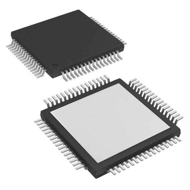


 工商网监
湘ICP备2023018690号
工商网监
湘ICP备2023018690号

