User's Guide
SLVUAT5 – November 2016
TPA3244 Evaluation Module
This user’s guide describes the operation of the evaluation module (TPA3244EVM, rev. B) for the
TPA3244 40-W Continuous/100-W Peak Stereo PurePath™ Ultra-HD Analog Input Power Stage. The
user’s guide also provides design information, which includes schematic, BOM, and PCB layout. For
questions and support, go to the E2E forums (e2e.ti.com).
The main contents of this document are:
• Hardware descriptions and implementation
• Design information
Related documents:
• TPA3244 data sheet (SLASEC6)
spacer
1
2
3
4
5
Contents
Hardware Overview.......................................................................................................... 3
1.1
TPA3244EVM Features ............................................................................................ 3
1.2
TPA3244EVM Frequency Adjust ................................................................................. 4
1.3
TPA3244EVM Single-Ended and Differential Input ............................................................ 4
1.4
TPA3244EVM Clip Overtemperature and Fault Indicators .................................................... 5
1.5
TPA3244EVM LC Filter ............................................................................................ 5
TPA3244EVM Setup ........................................................................................................ 7
2.1
TPA3244EVM Setup ............................................................................................... 7
2.2
Hardware Requirements ........................................................................................... 7
2.3
Hardware Default Setup BTL (2.0) ............................................................................... 8
Using the TPA3244EVM in Different Output Configurations ......................................................... 10
3.1
BTL Plus Two SE (2.1) Operation .............................................................................. 10
3.2
PBTL (0.1) Output Operation .................................................................................... 12
3.3
Single-Ended (SE) Output (4.0) Operation .................................................................... 13
Optional Inductors .......................................................................................................... 14
Board Layouts, Bill of Materials, and Schematic ....................................................................... 15
5.1
TPA3244EVM Board Layouts ................................................................................... 15
5.2
TPA3244EVM Board Dimension ................................................................................ 17
5.3
Bill of Materials .................................................................................................... 18
5.4
TPA3244EVM Schematic ........................................................................................ 21
List of Figures
1
TPA3244EVM ................................................................................................................ 3
2
Type-2 Filter for BD or AD Modulation .................................................................................... 5
3
TPA3244EVM LC Filter Cutoff Frequency
4
5
6
7
8
9
10
............................................................................... 6
TPA3244EVM Connections ................................................................................................ 7
TPA3245EVM THD + N vs Output Power 30 V, BTL 4 Ω, 600 kHz ................................................ 14
TPA3244EVM Top Composite Assembly ............................................................................... 15
TPA3244EVM Bottom Composite Assembly ........................................................................... 16
TPA3244EVM Board Dimension ......................................................................................... 17
TPA3244EVM Schematic 1 ............................................................................................... 21
TPA3244EVM Schematic 2 ............................................................................................... 22
SLVUAT5 – November 2016
Submit Documentation Feedback
TPA3244 Evaluation Module
Copyright © 2016, Texas Instruments Incorporated
1
�www.ti.com
11
TPA3244EVM Schematic 3 ............................................................................................... 23
List of Tables
1
Frequency Adjust Master Mode Selection ................................................................................ 4
2
Fault and Clip Overtemperature Status ................................................................................... 5
3
Stereo BTL Default Jumper States ........................................................................................ 8
4
Mode Selection Pins ....................................................................................................... 10
5
SE + 1 BTL Default Jumper States ...................................................................................... 10
6
PBTL Default Jumper States
7
SE 4.0 Default Jumper States ............................................................................................ 13
8
Bill of Materials
.............................................................................................
.............................................................................................................
12
18
Trademarks
PurePath is a trademark of Texas Instruments.
All other trademarks are the property of their respective owners.
2
TPA3244 Evaluation Module
SLVUAT5 – November 2016
Submit Documentation Feedback
Copyright © 2016, Texas Instruments Incorporated
�Hardware Overview
www.ti.com
1
Hardware Overview
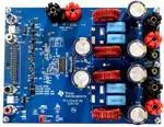
The TPA3244EVM PurePath™ Ultra-HD evaluation module demonstrates the TPA3244DDW integrated
circuit from Texas Instruments. The TPA3244DDW is a high-performance, high-power, class-D amplifier
that enables true premium sound quality with high-efficiency class-D technology. It features an advance
integrated feedback design and high-speed gate driver error correction (PurePath Ultra-HD), which
enables ultra-low distortion across the audio band and superior audio quality. This EVM supports two BTL
(stereo 2.0) output channels, one PBTL (mono 0.1) output channel, one BTL plus two SE (2.1) output
channels, and four SE (4.0) output channel configurations. The NE5532 is a high-performance audio op
amp designed to allow TPA3244DDW operation with differential or single-ended input signals to the EVM
with differential inputs yielding the optimal performance. The TPA3244EVM is a complete 2-VRMS analog
input 2 × 40-W continuous/2 × 100-W peak stereo high-power amplifier ready for evaluation and excellent
listening experience.
Figure 1. TPA3244EVM
1.1
TPA3244EVM Features
The TPA3244EVM has following features:
• Stereo PurePath Ultra-HD evaluation module
• Self-contained protection system (short circuit, clip, and thermal)
• Standard 4-VRMS differential input or 2-V single-ended line input
• BTL, PBTL, and SE output configuration support
• Frequency adjust and oscillator sync interface
• Single supply voltage range 14–31.5 V
• Double-sided, plated-through, 2-oz Cu, 2-layer PCB layout
SLVUAT5 – November 2016
Submit Documentation Feedback
TPA3244 Evaluation Module
Copyright © 2016, Texas Instruments Incorporated
3
�Hardware Overview
1.2
www.ti.com
TPA3244EVM Frequency Adjust
The TPA3244EVM offers hardware trimmed oscillator frequency by external control of the FREQ_ADJ pin.
The Frequency adjust can be used to reduce interference problems while using a radio receiver tuned
within the AM band, the switching frequency can be changed from nominal to lower values. These values
should be chosen such that the nominal and the lower value switching frequencies together results in the
fewest cases of interference throughout the AM band. The oscillator frequency can be selected by the
value of the FREQ_ADJ resistor connected to GND in master mode according to Table 1.
Table 1. Frequency Adjust Master Mode Selection
Master Mode
Resistor to GND
PWM Frequency
Nominal
10 kΩ
600 kHz
AM1
20 kΩ
500 kHz
AM2
30 kΩ
450 kHz
For slave-mode operation, turn off the oscillator by pulling the FREQ_ADJ pin to DVDD. This configures
the OSC_I/O pins as inputs to be slaved from an external differential clock. In a master/slave system interchannel delay is automatically set up between the switching phases of the audio channels, which can be
illustrated by no idle channels switching at the same time. This will not influence the audio output, but only
the switch timing to minimize noise coupling between audio channels through the power supply. This will
optimize audio performance and result in better operating conditions for the power supply. The interchannel delay will be set up for a slave device depending on the polarity of the OSC_I/O connection such
that slave mode 1 is selected by connecting the OSC_I/O of the master device with the OSC_I/O of the
slave device with the same polarity (+ to + and – to –), while slave mode 2 is selected by connecting the
OSC_I/O's with the inverse polarity (+ to – and – to +).
1.3
TPA3244EVM Single-Ended and Differential Input
The TPA3244EVM supports both differential and single-ended inputs. For single-ended inputs, J4 or J19
jumpers are set to the SE position, so that the TPA3244EVM uses the NE5532 to convert the singleended input signal to differential to properly drive the differential inputs of the TPA3244. The input RCA
jack, J3, is used to provide INA inputs and RCA jack J14 is used to provide INB inputs. RCA jack J18 is
used to provide INC inputs and RCA jack J15 is used to provide IND inputs with differential inputs.
For differential input operation, J4 or J19 jumpers are set to the DIFF position, and the TPA3244EVM uses
the NE5532 to buffer the differential input signal to the differential inputs of the TPA3244. The input RCA
jack, J3, is used to provide INA, RCA jack J14 provides INB, RCA jack J18 provides INC, and RCA jack
J15 provides IND with differential inputs.
NOTE: 1. Single-ended input settings on the TPA3244EVM should only be used for channels with
output configuration BTL or PBTL, not SE. However, for best performance, a differential input
should be used when in BTL or PBTL modes.wever, for best performance, a differential inpu
2. For SE output configuration J4 or J19 jumpers for that channel must be set to the DIFF
position, so the input signal INx is mapped directly to OUTx.
4
TPA3244 Evaluation Module
SLVUAT5 – November 2016
Submit Documentation Feedback
Copyright © 2016, Texas Instruments Incorporated
�Hardware Overview
www.ti.com
1.4
TPA3244EVM Clip Overtemperature and Fault Indicators
The TPA3244EVM is equipped with LED indicators that illuminate when the FAULT or CLIP_OTW pin
goes low. See Table 2 and the TPA3244 data sheet (SLASEC6) for more details.
Table 2. Fault and Clip Overtemperature Status
1.5
FAULT
CLIP_OTW
Description
0
0
Overtemperature (OTE) or overload (OLP) or undervoltage (UVP). Junction temperature higher
than 125°C (overtemperature warning).
0
0
Overload (OLP) or undervoltage (UVP). Junction temperature higher than 125°C (overtemperature
warning).
0
1
Overload (OLP) or undervoltage (UVP). Junction temperature lower than 125°C.
1
0
Junction temperature higher than 125°C (overtemperature warning)
1
1
Junction temperature lower than 125°C and no OLP or UVP faults (normal operation)
TPA3244EVM LC Filter
The TPA3244EVM is equipped 10-µH inductors and 1-µF capacitors for the output LC filter. These
components are setup as a Type-2 filter shown in Figure 2, since this allows the support of both BTL and
SE output configurations required for the EVM.
LBTL
Vout+
Cg
+
Vout
RBTL
_
Vout Cg
LBTL
Figure 2. Type-2 Filter for BD or AD Modulation
SLVUAT5 – November 2016
Submit Documentation Feedback
TPA3244 Evaluation Module
Copyright © 2016, Texas Instruments Incorporated
5
�Hardware Overview
www.ti.com
This filter has the following frequency response under the loading conditions listed in Figure 3.
Figure 3. TPA3244EVM LC Filter Cutoff Frequency
6
TPA3244 Evaluation Module
SLVUAT5 – November 2016
Submit Documentation Feedback
Copyright © 2016, Texas Instruments Incorporated
�TPA3244EVM Setup
www.ti.com
2
TPA3244EVM Setup
This section describes the TPA3244EVM hardware setup and connection.
2.1
TPA3244EVM Setup
Figure 4 illustrates the TPA3244EVM connections.
Figure 4. TPA3244EVM Connections
2.2
Hardware Requirements
The following hardware is required for this EVM:
• TPA3244EVM
• Power supply 5–14 A/14–31.5 VDC
• Two 2–8 Ω (approximately 200 W) speaker and resistor loads
• Four speaker/banana cables
• RCA input cables
• Analog output audio source
SLVUAT5 – November 2016
Submit Documentation Feedback
TPA3244 Evaluation Module
Copyright © 2016, Texas Instruments Incorporated
7
�TPA3244EVM Setup
2.3
www.ti.com
Hardware Default Setup BTL (2.0)
BTL (2.0) default hardware setup is as follows:
• Remove the EVM from the ESD bag.
• Check that jumpers are in their default state as shown in Figure 1 and Table 3 for stereo BTL
operation:
Table 3. Stereo BTL Default Jumper States
•
•
•
•
•
•
•
•
•
•
•
8
Jumper
Setting
J29
IN
Comment
PVDD to 15-V Buck
J31
IN
12-V LDO to 12-V terminal
J32
IN
3.3-V LDO to 3.3-V terminal
J33
IN
3.3-V LDO to 3.3-V terminal
J21
OUT
CSTART SE
J16
3 to 4
Master mode
J5
2 to 3
M1 – BTL
J6
2 to 3
M2 – BTL
J22
IN
OUTA capacitor shunt
J23
IN
OUTB capacitor shunt
J24
IN
OUTC capacitor shunt
J25
IN
OUTD capacitor shunt
J26
2 to 3
INC select
J27
2 to 3
IND select
J7
OUT
PBTL select INC
J8
OUT
PBTL select IND
J10
OUT
INC/D DIFF input
J12
OUT
INC/D DIFF input
J4
1 to 2
INA/B SE input
J19
1 to 2
INC/D SE input
Set S1 to the RESET position.
Set power supply to 30 V (14- to 31.5-V range) and current to 10 A (5- to 14-A range). Do not power
up until all connections are completed.
Connect power supply to TPA3244EVM positive terminal to PVDD (RED) and negative terminal to
GND (BLACK).
Connect left channel speaker/power resistor load (4–8 Ω) to TPA3244EVM positive output terminal to
OUTA (RED) and AP analog input channel A positive terminal.
Connect left channel speaker/power resistor load (4–8 Ω) to TPA3244EVM negative output terminal to
OUTB (BLACK) and AP analog input channel A negative terminal.
Connect right channel speaker/power resistor load (4–8 Ω) to TPA3244EVM positive output terminal to
OUTC (RED) and AP analog input channel B positive terminal.
Connect right channel speaker/power resistor load (4–8 Ω) to TPA3244EVM negative output terminal
to OUTD (BLACK) and AP analog input channel B negative terminal.
Be careful not to mix up PVDD and OUTA and OUTB terminals, since the colors are the same (RED).
For single-ended stereo inputs, connect AP channel A XLR to RCA male jacks to female RCA jacks
input A/AB (RED) and AP channel B XLR to RCA male jacks to female RCA jacks input C/CD (WHITE)
and set J4 and J19 jumper positions to SE.
For differential stereo inputs, connect the positive RCA male jacks to female RCA jack input A/AB
(RED) and input C/CD (WHITE) and connect negative RCA male jacks to female RCA jacks input B
(BLUE) and input D (BLACK) and set J4 and J19 jumper positions to DIFF.
Power up the power supply once all the connections are made correctly and the 3.3-V and 12-V LEDs
(GREEN) illuminate.
TPA3244 Evaluation Module
SLVUAT5 – November 2016
Submit Documentation Feedback
Copyright © 2016, Texas Instruments Incorporated
�TPA3244EVM Setup
www.ti.com
•
•
Set S1 to the NORMAL position.
CLIP_OTWz (ORANGE) and FAULTz (RED) LEDs should be off, if the audio source is off.
NOTE: J3/J10 and J18/J15 can be used for differential inputs to INA/INB and INC/IND, respectively.
Using a smart phone, tablet, or PC with headphone to RCA cable, audio streaming via headphone jack
can begin once the EVM is powered up correctly with jumpers in their default state. Start the media player
of your choice and enjoy the enhanced audio performance the TPA3244 provides as a quick check of the
setup.
SLVUAT5 – November 2016
Submit Documentation Feedback
TPA3244 Evaluation Module
Copyright © 2016, Texas Instruments Incorporated
9
�Using the TPA3244EVM in Different Output Configurations
3
www.ti.com
Using the TPA3244EVM in Different Output Configurations
The TPA3244EVM can be configured for four different output operations. The 2.0 BTL configuration is the
default setup of the TPA3244EVM described in Section 2.3. The remaining three configurations are 2.1
BTL plus two single-ended (SE) outputs, 0.1 PBTL output, and 4.0 single-ended (SE) outputs.
Table 4. Mode Selection Pins
Mode Pins
3.1
Input Mode
Output Configuration Description
M2
M1
0
0
2N + 1
2 × BTL
0
1
2N/1N + 1
1 × BTL + 2 × SE
1
0
2N + 1
1 × PBTL
1
1
1N + 1
4 × SE
Stereo BTL output configuration
2.1 BTL + SE mode. Channel AB: BTL, channel C + D: SE
Paralleled BTL configuration. Connect INPUT_C and INPUT_D to
GND.
Single-ended output configuration
BTL Plus Two SE (2.1) Operation
Configure the EVM as follows for 2 SE + 1 BTL operation:
Table 5. SE + 1 BTL Default Jumper States
•
•
•
•
•
•
10
Jumper
Setting
Comment
J29
IN
PVDD to 15-V Buck3
J31
IN
12-V LDO to 12-V terminal
J32
IN
3.3-V LDO to 3.3-V terminal
J33
IN
3.3-V LDO to 3.3-V terminal
J21
IN
CSTART SE
J16
3 to 4
Master mode
J5
1 to 2
M1 – 2XSE + BTL
J6
2 to 3
M2 - 2XSE + BTL
J22
IN
OUTA capacitor shunt
J23
IN
OUTB capacitor shunt
J24
OUT
OUTC capacitor shunt
J25
OUT
OUTD capacitor shunt
J26
2 to 3
INC select
J27
2 to 3
IND select
J7
OUT
PBTL select INC
J8
OUT
PBTL select IND
J10
OUT
INC/D DIFF input
J12
OUT
INC/D DIFF input
J4
1 to 2
INA/B SE input
J19
1 to 2
INC/D SE input
Set J6 to L and J5 to H.
Connect left (stereo) speaker/power resistor load (2–4 Ω) positive terminal to OUTC and remove
jumper J24.
Connect right (stereo) speaker/power resistor load (2–4 Ω) positive terminal to OUTD and remove
jumper J25.
Connect subwoofer (mono) speaker/power resistor load (4–8 Ω) positive terminal to OUTA and
negative terminal to OUTB.
Set J19 jumper position to DIFF.
Connect left (stereo) channel input to female RCA jack input C/CD (WHITE) for OUTC speaker.
TPA3244 Evaluation Module
SLVUAT5 – November 2016
Submit Documentation Feedback
Copyright © 2016, Texas Instruments Incorporated
�Using the TPA3244EVM in Different Output Configurations
www.ti.com
•
•
•
Connect right (stereo) channel input to female RCA jack input D (BLACK) for OUTD speaker.
For single-ended subwoofer (mono) input, connect RCA male jack to female RCA jack input A/AB
(RED) and set J4 jumper positions to SE.
For differential subwoofer (mono) inputs, connect positive RCA male jack to female RCA jack input
A/AB (RED) and connect negative RCA male jack to female RCA jack input B (YELLOW) and set J4
jumper positions to DIFF.
NOTE: OUTC and OUTD are the single-ended output channels and OUTA and OUTB are the BTL
channel for 2.1 operations.
SLVUAT5 – November 2016
Submit Documentation Feedback
TPA3244 Evaluation Module
Copyright © 2016, Texas Instruments Incorporated
11
�Using the TPA3244EVM in Different Output Configurations
3.2
www.ti.com
PBTL (0.1) Output Operation
Configure the EVM as follows for PBTL operations:
Table 6. PBTL Default Jumper States
•
•
•
•
•
•
Jumper
Setting
J29
IN
Comment
PVDD to 15-V Buck
J31
IN
12-V LDO to 12-V terminal
J32
IN
3.3-V LDO to 3.3-V terminal
J33
IN
3.3-V LDO to 3.3-V terminal
J21
OUT
CSTART SE
J16
3 to 4
Master mode
J5
2 to 3
M1 – PBTL
J6
1 to 2
M2 – PBTL
J22
IN
OUTA capacitor shunt
J23
IN
OUTB capacitor shunt
J24
IN
OUTC capacitor shunt
J25
IN
OUTD capacitor shunt
J26
2 to 3
INC select
J27
2 to 3
IND select
J7
2 to 3
PBTL select INC – GND
J8
2 to 3
PBTL select IND – GND
J10
OUT
INC/D DIFF input
J12
OUT
INC/D DIFF input
J4
1 to 2
INA/B SE input
J19
1 to 2
INC/D SE input
Set J6 to H and J5 to L.
Connect speaker/power resistor (2–4 Ω) positive terminal to OUTA and OUTC (OUT A and C shorted).
Connect speaker/power resistor (2–4 Ω) negative terminal to OUTB and OUTD (OUT B and D
shorted).
Install PBTL jumpers J7 and J8 (pulls input C and input D to GND).
For single-ended mono input, connect RCA male jack to female RCA jack input A/AB (RED) and set
J4 jumper positions to SE.
For differential mono inputs, connect positive RCA male jack to female RCA jack input A/AB (RED)
and connect negative RCA male jack to female RCA jack input B (YELLOW) and set J4 jumper
position to DIFF.
NOTE: INA and INB are the inputs for PBTL and INC and IND are grounded for PBTL operation.
12
TPA3244 Evaluation Module
SLVUAT5 – November 2016
Submit Documentation Feedback
Copyright © 2016, Texas Instruments Incorporated
�Using the TPA3244EVM in Different Output Configurations
www.ti.com
3.3
Single-Ended (SE) Output (4.0) Operation
Configure the EVM as follows for 4 single-ended operations:
Table 7. SE 4.0 Default Jumper States
•
•
•
•
•
•
•
•
•
•
Jumper
Setting
J29
IN
Comment
PVDD to 15-V Buck
J31
IN
12-V LDO to 12-V terminal
J32
IN
3.3-V LDO to 3.3-V terminal
J33
IN
3.3-V LDO to 3.3-V terminal
J21
IN
CSTART SE
J16
3 to 4
Master mode
J5
1 to 2
M1 – 4XSE
J6
1 to 2
M2 – 4XSE
J22
OUT
OUTA capacitor shunt
J23
OUT
OUTB capacitor shunt
J24
OUT
OUTC capacitor shunt
J25
OUT
OUTD capacitor shunt
J26
2 to 3
INC select
J27
2 to 3
IND select
J7
OUT
PBTL select INC
J8
OUT
PBTL select IND
J10
OUT
INC/D DIFF input
J12
OUT
INC/D DIFF input
J4
2 to 3
INA/B DIFF input
J19
2 to 3
INC/D DIFF input
Set J6 to H and J5 to H.
Connect speaker/power resistor (2–4 Ω) positive terminal to OUTA and Ground. Remove jumper J22.
Connect speaker/power resistor (2–4 Ω) positive terminal to OUTB and Ground. Remove jumper J23.
Connect speaker/power resistor (2–4 Ω) positive terminal to OUTC and Ground. Remove jumper J24.
Connect speaker/power resistor (2–4 Ω) positive terminal to OUTD and Ground. Remove jumper J25.
Set both J4 and J19 jumper positions to DIFF.
Connect input to female RCA jack input A/AB (RED) for OUTA speaker.
Connect input to female RCA jack input B (YELLOW) for OUTB speaker.
Connect input to female RCA jack input C/CD (WHITE) for OUTC speaker.
Connect input to female RCA jack input D (BLACK) for OUTD speaker.
NOTE: The performance of the TPA3244EVM/TPA3244 is dependent on the power supply. Design
the power supply with margins that can deliver the needed power. In low-frequency
applications, additional bulk capacitance may be needed. Replacing the bulk capacitors on
the TPA3244EVM with more capacitance may be necessary, depending on the power supply
used.
SLVUAT5 – November 2016
Submit Documentation Feedback
TPA3244 Evaluation Module
Copyright © 2016, Texas Instruments Incorporated
13
�Optional Inductors
4
www.ti.com
Optional Inductors
The TPA3244EVM includes component pads for optional output inductors L8 and L9. These pads fit
Coilcraft inductors UA8013-AL (7 µH) and UA8014-AL (10 µH). These dual-core inductors provide
extremely high performance in a small footprint to help shrink the solution size and cost. If using L8 and
L9, make sure to de-solder L2, L3, L4, and L5 first.
The plot in Figure 5 shows THD + N vs. output power for the TPA3245EVM (Pad-Up version of the
TPA3244) using the standard toroid inductors and the Coilcraft UA8013-AL (7 µH) and UA8014-AL (10
µH).
10
MA5172-AE 10 PH
UA8013-AL 7 PH Dual Inductor
UA8014-AL 10 PH Dual Inductor
THD + N (%)
1
0.1
0.01
0.001
0.01
0.1
1
10
100
Watts
200
D001
Figure 5. TPA3245EVM THD + N vs Output Power 30 V, BTL 4 Ω, 600 kHz
14
TPA3244 Evaluation Module
SLVUAT5 – November 2016
Submit Documentation Feedback
Copyright © 2016, Texas Instruments Incorporated
�Board Layouts, Bill of Materials, and Schematic
www.ti.com
5
Board Layouts, Bill of Materials, and Schematic
5.1
TPA3244EVM Board Layouts
Figure 6 and Figure 7 illustrate the board layouts for the EVM.
Figure 6. TPA3244EVM Top Composite Assembly
SLVUAT5 – November 2016
Submit Documentation Feedback
TPA3244 Evaluation Module
Copyright © 2016, Texas Instruments Incorporated
15
�Board Layouts, Bill of Materials, and Schematic
www.ti.com
Figure 7. TPA3244EVM Bottom Composite Assembly
16
TPA3244 Evaluation Module
SLVUAT5 – November 2016
Submit Documentation Feedback
Copyright © 2016, Texas Instruments Incorporated
�Board Layouts, Bill of Materials, and Schematic
www.ti.com
5.2
TPA3244EVM Board Dimension
Figure 8 illustrates the TPA3244EVM board dimensions 160 mm × 120 mm (image represented here is
not actual size).
Figure 8. TPA3244EVM Board Dimension
SLVUAT5 – November 2016
Submit Documentation Feedback
TPA3244 Evaluation Module
Copyright © 2016, Texas Instruments Incorporated
17
�Board Layouts, Bill of Materials, and Schematic
5.3
www.ti.com
Bill of Materials
Table 8 displays the BOM for this EVM.
Table 8. Bill of Materials
Designator
Qty
Value
!PCB1
1
C1
1
0.047uF
C2, C9, C13, C14,
C15, C22, C51, C67,
C68, C69, C72, C82,
C90
13
0.1uF
C3, C83, C84
3
1uF
C4
1
2.2uF
C5
1
C6
Description
Package Reference
Printed Circuit Board
Part Number
Manufacturer
AAP071
Any
CAP, CERM, 0.047 µF, 25 V, +/- 10%, X7R, 0402
0402
GRM155R71E473KA88D
Murata
CAP, CERM, 0.1 µF, 50 V, +/- 10%, X7R, 0603
0603
C0603C104K5RACTU
Kemet
CAP, CERM, 1 µF, 50 V, +/- 10%, X7R, 0603
0603
UMK107AB7105KA-T
Taiyo Yuden
CAP, CERM, 2.2 µF, 50 V, +/- 10%, X7R, 0805
0805
C2012X7R1H225K125AC
TDK
47uF
CAP, AL, 47 µF, 16 V, +/- 20%, 0.36 ohm, SMD
SMT Radial D
EEE-FK1C470P
Panasonic
1
4.7uF
CAP, CERM, 4.7 µF, 25 V, +/- 10%, X7R, 1206
1206
GRM31CR71E475KA88L
Murata
C7
1
5600pF
CAP, CERM, 5600 pF, 50 V, +/- 10%, X7R, 0603
0603
GRM188R71H562KA01D
Murata
C8, C50
2
0.47uF
CAP, CERM, 0.47 µF, 25 V, +/- 10%, X7R, 0603
0603
GRM188R71E474KA12D
Murata
C10
1
100uF
CAP, AL, 100 µF, 6.3 V, +/- 20%, 0.7 ohm, SMD
SMT Radial C
EEE-FK0J101UR
Panasonic
C11, C26, C37, C45,
C61
5
0.01uF
CAP, CERM, 0.01 µF, 50 V, +/- 10%, X7R, 0603
0603
C0603C103K5RACTU
Kemet
C12
1
4700pF
CAP, CERM, 4700 pF, 50 V, +/- 10%, X7R, 0603
0603
C0603X472K5RACTU
Kemet
C16, C53, C70, C81,
C89, C91
6
10uF
CAP, CERM, 10 µF, 16 V, +/- 10%, X5R, 0805
0805
EMK212BJ106KG-T
Taiyo Yuden
C17, C28, C55, C63
4
10uF
CAP, CERM, 10 µF, 16 V, +/- 10%, X7R, 1206
1206
GRM31CR71C106KAC7L
Murata
C18, C23, C57, C65
4
22pF
CAP, CERM, 22 pF, 50 V, +/- 5%, C0G/NP0, 0603
0603
GRM1885C1H220JA01D
Murata
C19, C30, C58, C64
4
100pF
CAP, CERM, 100 pF, 50 V, +/- 5%, C0G/NP0, 0603
0603
GRM1885C1H101JA01D
Murata
C20, C38, C62, C66,
C71
5
10uF
CAP, AL, 10 µF, 16 V, +/- 20%, 1.35 ohm, SMD
SMT Radial B
EEE-FK1C100R
Panasonic
C21, C34, C42, C56
4
1500uF
CAP, AL, 1500 µF, 63 V, +/- 20%, 0.03 ohm, AEC-Q200 Grade 2, TH
Dia 18mm
EEU-FC1J152
Panasonic
C24, C35, C43, C59
4
1uF
CAP, Film, 1 µF, 250 V, +/- 5%, TH
18x9.5x17.5mm
PHE426HB7100JR06
Kemet
C25, C36, C44, C60
4
1000pF
CAP, CERM, 1000 pF, 50 V, +/- 1%, C0G/NP0, 0603
0603
GRM1885C1H102FA01J
Murata
C27, C29, C52, C54
4
0.033uF
CAP, CERM, 0.033 µF, 25 V, +/- 10%, X7R, 0603
0603
GRM188R71E333KA01D
Murata
C31, C46
2
2200uF
CAP, AL, 2200 µF, 50 V, +/- 20%, 0.023 ohm, AEC-Q200 Grade 2, TH
Dia 18mm
EEU-FC1H222
Panasonic
C32, C33, C47, C48
4
1uF
CAP, CERM, 1 µF, 50 V, +/- 10%, X7R, 1206
1206
GRM31MR71H105KA88L
Murata
C39
1
47uF
CAP, AL, 47 µF, 50 V, +/- 20%, 0.68 ohm, SMD
SMT Radial E
EEE-FK1H470P
Panasonic
C40, C41
2
1uF
CAP, CERM, 1 µF, 16 V, +/- 10%, X7R, 0603
0603
GRM188R71C105KA12D
Murata
C49
1
0.047uF
CAP, CERM, 0.047 µF, 50 V, +/- 10%, X7R, 0603
0603
GRM188R71H473KA61D
Murata
D1
1
100V
Diode, Schottky, 100 V, 1 A, SMA
SMA
B1100-13-F
Diodes Inc.
D2
1
Orange
LED, Orange, SMD
LED_0805
LTST-C170KFKT
Lite-On
D3
1
100V
Diode, Schottky, 100 V, 3 A, SMA
SMA
SK310A-TP
Micro Commercial Components
D4
1
Red
LED, Red, SMD
Red 0805 LED
LTST-C170KRKT
Lite-On
D5, D6
2
Green
LED, Green, SMD
LED_0805
LTST-C171GKT
Lite-On
H1, H2, H3, H4, H5
5
MACHINE SCREW PAN PHILLIPS M3
M3 Screw
RM3X8MM 2701
APM HEXSEAL
H6, H7, H8, H9, H10
5
Standoff, Hex,25mm Length, M3, Aluminum
Standoff M3
24438
Keystone
18
TPA3244 Evaluation Module
SLVUAT5 – November 2016
Submit Documentation Feedback
Copyright © 2016, Texas Instruments Incorporated
�Board Layouts, Bill of Materials, and Schematic
www.ti.com
Table 8. Bill of Materials (continued)
Designator
Description
Package Reference
Part Number
Manufacturer
J1, J2, J9
Qty
3
Value
Dual Binding Posts with Base, 2x1, TH
Dual Binding Posts with Base,
2x1, TH
6883
Pomona Electronics
J3
1
RCA Jack, Vertical, Red, TH
RCA JACK, RED
RCJ-022
CUI Inc.
J4, J5, J6, J19, J26,
J27
6
Header, 100mil, 3x1, Gold, TH
PBC03SAAN
PBC03SAAN
Sullins Connector Solutions
J7, J8, J21, J29,
J30, J32, J33
7
Header, 100mil, 2x1, Gold, TH
Sullins 100mil, 1x2, 230 mil
above insulator
PBC02SAAN
Sullins Connector Solutions
J10, J12
2
Header, 2.54 mm, 3x1, TH
Header, 2.54mm, 3x1, TH
22-11-2032
Molex
J11, J20
2
Binding Post, BLACK, TH
11.4x27.2mm
7007
Keystone
J14
1
RCA Jack, Vertical, Black, TH
RCA Jack, Vertical, Black, TH
RCJ-021
CUI Inc.
J15
1
RCA Jack, Vertical, Blue, TH
RCA Jack, Vertical, Blue, TH
RCJ-025
CUI Inc.
J16
1
Header, 100mil, 4x2, Tin, TH
Header, 4x2, 100mil, Tin
PEC04DAAN
Sullins Connector Solutions
J17
1
Header (friction lock), 100mil, 4x1, Gold, TH
Header 4x1 keyed
0022112042
Molex
J18
1
RCA Jack, Vertical, White, TH
RCA JACK, WHITE
RCJ-023
CUI Inc.
J22, J23, J24, J25,
J31
5
JUMPER TIN SMD
6.85x0.97x2.51 mm
S1911-46R
Harwin
J28
1
Receptacle, 100mil, 14x2, Gold, TH
14x2 Receptacle
SSW-114-01-G-D
Samtec
L1
1
100uH
Inductor, Shielded Drum Core, Ferrite, 100 µH, 1.5 A, 0.165 ohm, SMD
SMD
7447714101
Wurth Elektronik
L2, L3, L4, L5
4
10uH
Inductor, Toroid, Powdered Iron, 10 µH, 6.1 A, 0.026 ohm, TH
28.6x12.3mm
MA5172-AE
Coilcraft
L6
1
10uH
Inductor, Wirewound, 10 µH, 0.8 A, 0.204 ohm, SMD
2-Pin SMD, Body 4 x 4 mm,
Height 1.2 mm
NRS4012T100MDGJV
Taiyo Yuden
L7
1
10uH
Inductor, Wirewound, 10 µH, 0.08 A, 0.36 ohm, SMD
0603
GLFR1608T100M-LR
TDK
Q1, Q2
2
60V
MOSFET, N-CH, 60 V, 0.17 A, SOT-23
SOT-23
2N7002-7-F
Diodes Inc.
R1, R3, R4, R12,
R30, R44, R46
7
0
RES, 0, 5%, 0.1 W, 0603
0603
CRCW06030000Z0EA
Vishay-Dale
R2
1
182k
RES, 182 k, 1%, 0.125 W, 0805
0805
ERJ-6ENF1823V
Panasonic
R5, R10, R19, R23,
R33, R35
6
100
RES, 100, 1%, 0.1 W, 0603
0603
CRCW0603100RFKEA
Vishay-Dale
R6
1
100k
RES, 100 k, 1%, 0.1 W, 0603
0603
CRCW0603100KFKEA
Vishay-Dale
R7, R8, R20, R21,
R25, R27, R37, R38,
R41, R42
10
10.0k
RES, 10.0 k, 0.1%, 0.1 W, 0603
0603
RT0603BRD0710KL
Yageo America
R9, R43, R45, R48
4
100k
RES, 100 k, 1%, 0.063 W, 0402
0402
CRCW0402100KFKED
Vishay-Dale
R11, R14, R18, R22
4
3.3
RES, 3.3, 5%, 0.1 W, 0603
0603
CRCW06033R30JNEA
Vishay-Dale
R13
1
22.0k
RES, 22.0 k, 1%, 0.1 W, 0603
0603
RC0603FR-0722KL
Yageo America
R15
1
30.0k
RES, 30.0 k, 1%, 0.1 W, 0603
0603
RC0603FR-0730KL
Yageo America
R16
1
20.0k
RES, 20.0 k, 1%, 0.1 W, 0603
0603
RC0603FR-0720KL
Yageo America
R17, R36, R52
3
10.0k
RES, 10.0 k, 1%, 0.1 W, 0603
0603
CRCW060310K0FKEA
Vishay-Dale
R24, R28
2
47k
RES, 47 k, 5%, 0.1 W, 0603
0603
RC0603JR-0747KL
Yageo America
R26
1
3.30k
RES, 3.30 k, 1%, 0.1 W, 0603
0603
RC0603FR-073K3L
Yageo America
R29, R31
2
1.00k
RES, 1.00 k, 1%, 0.1 W, 0603
0603
CRCW06031K00FKEA
Vishay-Dale
R32
1
9.10k
RES, 9.10 k, 1%, 0.1 W, 0603
0603
RC0603FR-079K1L
Yageo America
R34
1
360
RES, 360, 5%, 0.063 W, 0402
0402
CRCW0402360RJNED
Vishay-Dale
SLVUAT5 – November 2016
Submit Documentation Feedback
TPA3244 Evaluation Module
Copyright © 2016, Texas Instruments Incorporated
19
�Board Layouts, Bill of Materials, and Schematic
www.ti.com
Table 8. Bill of Materials (continued)
Designator
Qty
Value
Description
Package Reference
Part Number
Manufacturer
R39
1
4.99k
RES, 4.99 k, 1%, 0.063 W, 0402
0402
CRCW04024K99FKED
Vishay-Dale
R40
1
1.00k
RES, 1.00 k, 1%, 0.063 W, 0402
0402
CRCW04021K00FKED
Vishay-Dale
R57
1
1.00k
RES, 1.00 k, 1%, 0.1 W, 0402
0402
ERJ-2RKF1001X
Panasonic
R58
1
1.50k
RES, 1.50 k, 1%, 0.063 W, 0402
0402
CRCW04021K50FKED
Vishay-Dale
S1
1
Switch, SPDT, On-On, 2 Pos, TH
Switch, 7x4.5mm
200USP1T1A1M2RE
E-Switch
SH1, SH2, SH3,
SH4, SH5, SH6,
SH7, SH8, SH9,
SH10, SH11, SH12,
SH13
13
Shunt, 100mil, Gold plated, Black
Shunt
969102-0000-DA
3M
U1
1
High Voltage 1A Step Down Switching Regulator, 10-pin LLP, Pb-Free
SDC10A
LM5010ASD/NOPB
Texas Instruments
U2
1
1A Low Dropout Regulator, 4-pin SOT-223, Pb-Free
MP04A
LM2940IMP-12/NOPB
Texas Instruments
U3
1
FIXED LOW-DROPOUT VOLTAGE REGULATOR, DCY0004A
DCY0004A
TLV1117-33IDCY
Texas Instruments
U4
1
40-W Stereo, 100-W peak PurePath™ Ultra-HD Pad Down Class-D Amplifier, DDW0044D
DDW0044D
TPA3244DDWR
Texas Instruments
U5, U6
2
Dual Low-Noise Operational Amplifier, 10 to 30 V, 0 to 70 degC, 8-pin SOIC (D0008A),
Green (RoHS & no Sb/Br)
D0008A
NE5532ADR
Texas Instruments
U7
1
ULTRA-SMALL SUPPLY VOLTAGE SUPERVISORS, DCK0005A
DCK0005A
TPS3802K33DCKR
Texas Instruments
C73, C74, C75, C76
0
22pF
CAP, CERM, 22 pF, 50 V, +/- 5%, C0G/NP0, 0603
0603
GRM1885C1H220JA01D
Murata
C77, C78, C79, C80
0
1uF
CAP, CERM, 1 µF, 50 V, +/- 10%, X7R, 1206
1206
GRM31MR71H105KA88L
Murata
C85, C86, C87, C88
0
1000pF
CAP, CERM, 1000 pF, 50 V, +/- 1%, C0G/NP0, 0603
0603
GRM1885C1H102FA01J
Murata
FID1, FID2, FID3,
FID4, FID5, FID6
0
Fiducial mark. There is nothing to buy or mount.
N/A
N/A
N/A
J13
0
Header, 100mil, 2x1, Gold, TH
Sullins 100mil, 1x2, 230 mil
above insulator
PBC02SAAN
Sullins Connector Solutions
L8, L9
0
5uH
Coupled inductor, 5 µH, 16.6 A, 0.006 ohm, SMD
15.5x14mm
RA7231-ALB
Coilcraft
R47, R49, R50, R51
0
18.0k
RES, 18.0 k, 1%, 0.1 W, 0603
0603
RC0603FR-0718KL
Yageo America
R53, R54, R55, R56
0
2.7
RES, 2.7, 5%, 3 W, SM_3, 10.5x5x5.5mm
SM_3, 10.5x5x5.5mm
SMW32R7JT
TE Connectivity
R59, R60, R61, R62
0
10.0
RES, 10.0, 1%, 0.1 W, 0603
0603
CRCW060310R0FKEA
Vishay-Dale
R63, R64, R65, R66
0
0
RES, 0, 5%, 0.1 W, 0603
0603
CRCW06030000Z0EA
Vishay-Dale
R67
0
0
RES, 0, 5%, 0.125 W, 0805
0805
ERJ-6GEY0R00V
Panasonic
TP1, TP2, TP3, TP4,
TP5, TP6, TP7, TP8,
TP9, TP10, TP11,
TP12, TP13, TP14
0
Test Point, Multipurpose, Grey, TH
Grey Multipurpose Testpoint
5128
Keystone
TP15,
TP18,
TP21,
TP24,
TP27,
0
Testpoint
Test Point, 0.45mm hole size
TP_H0.45P0.75
Texas Instruments
20
TP16,
TP19,
TP22,
TP25,
TP28
TP17,
TP20,
TP23,
TP26,
1x2
TPA3244 Evaluation Module
SLVUAT5 – November 2016
Submit Documentation Feedback
Copyright © 2016, Texas Instruments Incorporated
�Board Layouts, Bill of Materials, and Schematic
www.ti.com
5.4
TPA3244EVM Schematic
The schematics for TPA3244EVM are illustrated in Figure 9 through Figure 11.
C18
C20
LEFT+
INA-RCA
R9
INPUT SE A
SE AB
DIFF A+
GND


 工商网监
湘ICP备2023018690号
工商网监
湘ICP备2023018690号
