CY7C166
16 K × 4 Static RAM
16 K × 4 Static RAM
Features
Functional Description
The CY7C166 is a high-performance CMOS static RAMs
organized as 16,384 by 4 bits. Easy memory expansion is
provided by an active LOW Chip Enable (CE) and tri-state
drivers. The CY7C166 has an active LOW Output Enable (OE)
feature. This device has an automatic power-down feature,
reducing the power consumption by 65% when deselected.
■
High speed
❐ 15 ns
■
Output enable (OE) feature
■
CMOS for optimum speed/power
■
Low active power
❐ 633 mW
■
Low standby power
❐ 110 mW
■
TTL-compatible inputs and outputs
■
Automatic power-down when deselected
Writing to the device is accomplished when the Chip Enable (CE)
and Write Enable (WE) inputs are both LOW (and the Output
Enable (OE) is LOW). Data on the four input/output pins (I/O0
through I/O3) is written into the memory location specified on the
address pins (A0 through A13).
Reading the device is accomplished by taking Chip Enable (CE)
LOW (and OE LOW), while Write Enable (WE) remains HIGH.
Under these conditions the contents of the memory location
specified on the address pins will appear on the four data I/O
pins.
The I/O pins stay in a high-impedance state when Chip Enable
(CE) is HIGH (or Output Enable (OE) is HIGH). A die coat is used
to insure alpha immunity.
Logic Block Diagram
16K x 4
ARRAY
I/O1
I/O0
CE
WE
(OE)
A13
A0
A9
A10
A11
A12
•
I/O2
POWER
DOWN
COLUMN
DECODER
Cypress Semiconductor Corporation
Document #: 38-05025 Rev. *C
I/O3
SENSE AMPS
A1
A2
A3
A4
A5
A6
A7
A8
ROW DECODER
INPUT BUFFER
198 Champion Court
•
San Jose, CA 95134-1709
•
408-943-2600
Revised November 29, 2010
[+] Feedback
�CY7C166
Contents
Pin Configuration ............................................................. 3
Selection Guide ................................................................ 3
Maximum Ratings ............................................................. 4
Operating Range ............................................................... 4
Electrical Characteristics ................................................. 4
Capacitance ...................................................................... 4
AC Test Loads and Waveforms ....................................... 5
Switching Characteristics ................................................ 5
Switching Waveforms ...................................................... 6
Read Cycle No. 1 ........................................................ 6
Read Cycle No. 2 ........................................................ 6
Write Cycle No. 1(WE Controlled) ............................... 7
Write Cycle No. 2(CE Controlled) ................................ 7
Typical DC and AC Characteristics ................................ 8
Document #: 38-05025 Rev. *C
CY7C166 Truth Table ....................................................... 9
Address Designators ....................................................... 9
Ordering Information ........................................................ 9
Ordering Code Definitions ........................................... 9
Package Diagram ............................................................ 10
Acronyms ........................................................................ 10
Document Conventions ................................................. 10
Units of Measure ....................................................... 10
Document History Page ................................................. 11
Sales, Solutions, and Legal Information ...................... 12
Worldwide Sales and Design Support ....................... 12
Products .................................................................... 12
PSoC Solutions ......................................................... 12
Page 2 of 12
[+] Feedback
�CY7C166
Pin Configuration
SOJ
Top View
A5
A6
A7
A8
A9
A10
A11
A12
A13
CE
OE
GND
1
24
2
23
3
22
4
21
5
20
6 7C166 19
18
7
17
8
9
16
10
15
11
14
12
13
VCC
A4
A3
A2
A1
A0
NC
I/O3
I/O2
I/O1
I/O0
WE
Selection Guide
Description
CY7C166-15
Maximum Access Time (ns)
15
Maximum Operating Current (mA)
115
Maximum CMOS Standby Current (mA)
20
Document #: 38-05025 Rev. *C
Page 3 of 12
[+] Feedback
�CY7C166
Maximum Ratings
Exceeding the maximum ratings may impair the useful life of the
device. These user guidelines are not tested.
Storage temperature ................................ –65 °C to +150 °C
Ambient temperature with
power applied ........................................... –55 °C to +125 °C
Supply voltage to ground potential ...............–0.5 V to +7.0 V
Output current into outputs (LOW) .............................. 20 mA
Static discharge voltage.......................................... > 2001 V
(per MIL-STD-883, method 3015)
Latch-up current .................................................... > 200 mA
Operating Range
DC voltage applied to outputs
in high Z State[1] ...........................................–0.5 V to +7.0 V
[1]
DC input voltage ........................................–0.5 V to +7.0 V
Range
Ambient
Temperature
VCC
Commercial
0 °C to +70 °C
5 V 10%
Electrical Characteristics
Over the Operating Range
–15
Parameter
Description
Test Conditions
VOH
Output HIGH voltage
VCC = Min, IOH = –4.0 mA
VOL
Output LOW voltage
VCC = Min, IOL = 8.0 mA
VIH
Input HIGH voltage
voltage[1]
Min
Max
Unit
2.4
–
V
–
0.4
V
2.2
VCC
V
–0.5
0.8
V
+5
A
VIL
Input LOW
IIX
Input leakage current
GND < VI < VCC
–5
IOZ
Output leakage current
GND < VO < VCC, output disabled
–5
+5
A
ICC
VCC operating supply current
VCC = Max, IOUT = 0 mA
–
115
mA
ISB1
Automatic CE
power-down current[2]
Max VCC, CE > VIH,
Min Duty Cycle = 100%
–
40
mA
ISB2
Automatic CE
power-down current[2]
Max VCC, CE > VCC – 0.3 V,
VIN > VCC – 0.3 V or VIN < 0.3 V
–
20
mA
Capacitance[3]
Parameter
Description
CIN
Input capacitance
COUT
Output capacitance
Test Conditions
TA = 25 °C, f = 1 MHz,
VCC = 5.0 V
Max
Unit
10
pF
10
pF
Notes
1. Minimum voltage is equal to –3.0 V for pulse durations less than 30 ns.
2. A pull-up resistor to VCC on the CE input is required to keep the device deselected during VCC power-up, otherwise ISB will exceed values given.
3. Tested initially and after any design or process changes that may affect these parameters.
Document #: 38-05025 Rev. *C
Page 4 of 12
[+] Feedback
�CY7C166
AC Test Loads and Waveforms
R1 481
5V
OUTPUT
R1 481
5V
OUTPUT
30 pF
R2
255
INCLUDING
JIG AND
SCOPE (a)
ALL INPUT PULSES
3.0 V
5 pF
INCLUDING
JIG AND
SCOPE (b)
R2
255
GND
90%
10%
90%
10%
< 5 ns
< 5 ns
C164–5
Equivalent to:
THÉVENIN EQUIVALENT
167
OUTPUT
1.73 V
Switching Characteristics
Over the Operating Range[4]
CY7C166-15
Parameter
Description
Min
Max
Unit
READ CYCLE
tRC
Read cycle time
15
–
ns
tAA
Address to data valid
–
15
ns
tOHA
Output hold from address change
3
–
ns
tACE
CE LOW to data valid
–
15
ns
tDOE
OE LOW to data valid
–
10
ns
tLZOE
OE LOW to low Z
3
–
ns
tHZOE
OE HIGH to high Z
–
8
ns
tLZCE
CE LOW to low Z[5]
3
–
ns
–
8
ns
Z[5, 6]
tHZCE
CE HIGH to high
tPU
CE LOW to power-up
0
–
ns
tPD
CE HIGH to power-down
–
15
ns
tWC
Write cycle time
15
–
ns
tSCE
CE LOW to write end
12
–
ns
tAW
Address set-up to write end
12
–
ns
tHA
Address hold from write end
0
–
ns
tSA
Address set-up to write start
0
–
ns
tPWE
WE pulse width
12
–
ns
tSD
Data set-up to write end
10
–
ns
tHD
Data hold from write end
0
–
ns
WE HIGH to low
Z[5]
5
–
ns
WE LOW to high
Z[5, 6]
–
7
ns
WRITE CYCLE[7]
tLZWE
tHZWE
Notes
4. Test conditions assume signal transition time of 5 ns or less, timing reference levels of 1.5 V, input pulse levels of 0 to 3.0 V, and output loading of the specified
IOL/IOH and 30 pF load capacitance.
5. At any given temperature and voltage condition, tHZCE is less than tLZCE for any given device. These parameters are guaranteed by design and not 100% tested.
6. tHZCE and tHZWE are specified with CL = 5 pF as in part (b) in AC Test Loads. Transition is measured 500 mV from steady-state voltage.
7. The internal write time of the memory is defined by the overlap of CE LOW and WE LOW. Both signals must be LOW to initiate a write and either signal can terminate a
write by going HIGH. The data input set-up and hold timing should be referenced to the rising edge of the signal that terminates the write.
Document #: 38-05025 Rev. *C
Page 5 of 12
[+] Feedback
�CY7C166
Switching Waveforms
Read Cycle No. 1[8, 9]
tRC
ADDRESS
tOHA
DATA OUT
tAA
PREVIOUS DATA VALID
DATA VALID
Read Cycle No. 2[8, 10]
tRC
CE
tACE
OE
7C166
tHZOE
tHZCE
tDOE
DATA OUT
tLZOE
HIGH IMPEDANCE
tLZCE
V CC
SUPPLY
CURRENT
HIGH
IMPEDANCE
DATA VALID
tPD
tPU
50%
50%
ICC
ISB
Notes
8. WE is HIGH for read cycle.
9. Device is continuously selected, CE = VIL. (CY7C166: OE = VIL also).
10. Address valid prior to or coincident with CE transition LOW.
Document #: 38-05025 Rev. *C
Page 6 of 12
[+] Feedback
�CY7C166
Switching Waveforms (continued)
Write Cycle No. 1(WE Controlled)[11,12]
tWC
ADDRESS
tSCE
CE
tSA
tAW
tHA
tPWE
WE
tSD
tHD
DATAINVALID
DATA IN
tHZWE
DATA I/O
tLZWE
HIGH IMPEDANCE
DATA UNDEFINED
Write Cycle No. 2(CE Controlled)[11,12,13]
tWC
ADDRESS
tSA
tSCE
CE
tAW
tHA
tPWE
WE
tSD
DATA IN
DATA I/O
tHD
DATAIN VALID
HIGH IMPEDANCE
Notes
11. The internal write time of the memory is defined by the overlap of CE LOW and WE LOW. Both signals must be LOW to initiate a write and either signal can terminate
a write by going HIGH. The data input set-up and hold timing should be referenced to the rising edge of the signal that terminates the write.
12. CY7C166 only: Data I/O will be high-impedance if OE = VIH.
13. If CE goes HIGH simultaneously with WE HIGH, the output remains in a high-impedance state.
Document #: 38-05025 Rev. *C
Page 7 of 12
[+] Feedback
�CY7C166
Typical DC and AC Characteristics
SB
1.2
1.2
I CC
0.8
0.6
0.4
4.5
5.0
0.8
0.6
0.4
V CC = 5.0V
V IN = 5.0V
5.5
6.0
I SB
0.0
–55
25
NORMALIZED ACCESS TIME
vs. AMBIENT TEMPERATURE
1.4
1.6
1.3
1.4
NORMALIZED tAA
NORMALIZED t AA
NORMALIZED ACCESS TIME
vs. SUPPLY VOLTAGE
1.2
TA = 25°C
1.0
1.2
1.0
VCC =5.0V
0.8
0.9
0.8
4.0
4.5
5.0
5.5
0.6
–55
6.0
3.0
30.0
2.5
25.0
2.0
1.5
1.0
25
3.0
4.0
SUPPLY VOLTAGE (V)
Document #: 38-05025 Rev. *C
40
20
0
0.0
1.0
15.0
10.0
VCC = 4.5V
TA = 25°C
5.0
0.0
0
200
400
600
800 1000
CAPACITANCE (pF)
3.0
4.0
140
OUTPUT SINK CURRENT
vs. OUTPUT VOLTAGE
120
100
VCC = 5.0V
TA =25°C
80
60
40
20
0
0.0
125
20.0
2.0
OUTPUT VOLTAGE (V)
1.0
2.0
3.0
4.0
OUTPUT VOLTAGE (V)
NORMALIZED I CC vs. CYCLE TIME
1.25
5.0
0.5
2.0
V CC = 5.0V
TA = 25°C
60
TYPICAL ACCESS TIME CHANGE
vs. OUTPUT LOADING
DELTA tAA (ns)
NORMALIZED I PO
TYPICAL POWER-ON CURRENT
vs. SUPPLY VOLTAGE
1.0
80
AMBIENT TEMPERATURE (°C)
SUPPLY VOLTAGE (V)
0.0
0.0
100
AMBIENT TEMPERATURE (°C)
SUPPLY VOLTAGE (V)
1.1
125
120
OUTPUT SINK CURRENT (mA)
0.0
4.0
I CC
0.2
I SB
0.2
1.0
OUTPUT SOURCE CURRENT
vs. OUTPUT VOLTAGE
NORMALIZED I CC
1.0
NORMALIZED I,CC
I
NORMALIZED I,CC
I
SB
1.4
NORMALIZED SUPPLY CURRENT
vs. AMBIENT TEMPERATURE
OUTPUT SOURCE CURRENT (mA)
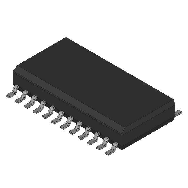
Figure 1. 24-pin (300-mil) SOJ (51-85030)
NORMALIZED SUPPLY CURRENT
vs. SUPPLY VOLTAGE
VCC = 5.0V
TA = 25°C
VIN = 0.5V
1.00
0.75
0.50
10
20
30
40
CYCLE FREQUENCY (MHz)
Page 8 of 12
[+] Feedback
�CY7C166
CY7C166 Truth Table
CE
WE
OE
Input/Output
Mode
Power
H
X
X
High Z
Deselect/power-down
Standby (ISB)
L
H
L
Data out
Read
Active (ICC)
L
L
H
Data in
Write
Active (ICC)
L
H
H
High Z
Select/output disabled
Active (ICC)
Address Designators
Address
Name
Address
Function
CY7C166 Pin
Number
A5
X3
1
A6
X4
2
A7
X5
3
A8
X6
4
A9
X7
5
A10
Y5
6
A11
Y4
7
A12
Y0
8
A13
Y1
9
A0
Y2
19
A1
Y3
20
A2
X0
21
A3
X1
22
A4
X2
23
Ordering Information
Speed
(ns)
15
Ordering Code
CY7C166-15VC
Package
Diagram
Package Type
51-85030
24-pin (300-Mil) Molded SOJ
Operating
Range
Commercial
Ordering Code Definitions
CY 7C 166 - 15
V C
C = Temperature range (Commercial)
V = 24-pin (300-Mil) Molded SOJ
15 = Speed grade
Part Identifier
Family: 7C = Fast asynchronous SRAM
Company ID: CY = Cypress
Document #: 38-05025 Rev. *C
Page 9 of 12
[+] Feedback
�CY7C166
Package Diagram
Figure 1. 24-pin (300-mil) SOJ, 51-85030
51-85030 *C
Acronyms
Document Conventions
Acronym
Description
CMOS
complementary metal oxide semiconductor
CE
chip enable
DIP
dual inline package
I/O
input/output
OE
output enable
SRAM
static random access memory
SOJ
small outline J-lead
TTL
WE
Units of Measure
Symbol
Unit of Measure
ns
nano seconds
V
Volts
µA
micro Amperes
mA
milli Amperes
mV
milli Volts
transistor-transistor logic
mW
milli Watts
write enable
pF
pico Farad
°C
degree Celcius
W
Watts
%
percent
Document #: 38-05025 Rev. *C
Page 10 of 12
[+] Feedback
�CY7C166
Document History Page
Document Title: CY7C166 16 K × 4 Static RAM
Document Number: 38-05025
REV.
ECN NO.
of
Issue Date Orig.
Change
Description of Change
**
106811
09/10/01
SZV
Change from Spec number: 38-00032 to 38-05025
*A
486744
See ECN
NXR
Removed 20 ns and 35 ns speed bin from Product offering
Removed 24-pin (300-Mil) Molded DIP package
Changed the description of IIX from Input Load Current to Input Leakage
Current in DC Electrical Characteristics table
Removed IOS parameter from DC Electrical Characteristics table
Updated the ordering information table
*B
2894113
03/17/2010
VKN
Added Table of Contents
Removed CY7C164 part from the data sheet
Removed 25 ns speed bin
Removed 22-pin (300-Mil) PDIP package
Updated ordering Information Table
Updated Package Diagram (Figure 1)
Added Sales, Solutions, and Legal Information
*C
3096933
11/29/2010
PRAS
Document #: 38-05025 Rev. *C
Added Ordering Code Definitions.
Added Acronyms and Units of Measure.
Minor edits.
Page 11 of 12
[+] Feedback
�CY7C166
Sales, Solutions, and Legal Information
Worldwide Sales and Design Support
Cypress maintains a worldwide network of offices, solution centers, manufacturer’s representatives, and distributors. To find the office
closest to you, visit us at Cypress Locations.
Products
Automotive
Clocks & Buffers
Interface
Lighting & Power Control
PSoC Solutions
cypress.com/go/automotive
cypress.com/go/clocks
psoc.cypress.com/solutions
cypress.com/go/interface
PSoC 1 | PSoC 3 | PSoC 5
cypress.com/go/powerpsoc
cypress.com/go/plc
Memory
Optical & Image Sensing
PSoC
Touch Sensing
USB Controllers
Wireless/RF
cypress.com/go/memory
cypress.com/go/image
cypress.com/go/psoc
cypress.com/go/touch
cypress.com/go/USB
cypress.com/go/wireless
© Cypress Semiconductor Corporation, 2001-2010. The information contained herein is subject to change without notice. Cypress Semiconductor Corporation assumes no responsibility for the use of
any circuitry other than circuitry embodied in a Cypress product. Nor does it convey or imply any license under patent or other rights. Cypress products are not warranted nor intended to be used for
medical, life support, life saving, critical control or safety applications, unless pursuant to an express written agreement with Cypress. Furthermore, Cypress does not authorize its products for use as
critical components in life-support systems where a malfunction or failure may reasonably be expected to result in significant injury to the user. The inclusion of Cypress products in life-support systems
application implies that the manufacturer assumes all risk of such use and in doing so indemnifies Cypress against all charges.
Any Source Code (software and/or firmware) is owned by Cypress Semiconductor Corporation (Cypress) and is protected by and subject to worldwide patent protection (United States and foreign),
United States copyright laws and international treaty provisions. Cypress hereby grants to licensee a personal, non-exclusive, non-transferable license to copy, use, modify, create derivative works of,
and compile the Cypress Source Code and derivative works for the sole purpose of creating custom software and or firmware in support of licensee product to be used only in conjunction with a Cypress
integrated circuit as specified in the applicable agreement. Any reproduction, modification, translation, compilation, or representation of this Source Code except as specified above is prohibited without
the express written permission of Cypress.
Disclaimer: CYPRESS MAKES NO WARRANTY OF ANY KIND, EXPRESS OR IMPLIED, WITH REGARD TO THIS MATERIAL, INCLUDING, BUT NOT LIMITED TO, THE IMPLIED WARRANTIES
OF MERCHANTABILITY AND FITNESS FOR A PARTICULAR PURPOSE. Cypress reserves the right to make changes without further notice to the materials described herein. Cypress does not
assume any liability arising out of the application or use of any product or circuit described herein. Cypress does not authorize its products for use as critical components in life-support systems where
a malfunction or failure may reasonably be expected to result in significant injury to the user. The inclusion of Cypress’ product in a life-support systems application implies that the manufacturer
assumes all risk of such use and in doing so indemnifies Cypress against all charges.
Use may be limited by and subject to the applicable Cypress software license agreement.
Document #: 38-05025 Rev. *C
Revised November 29, 2010
Page 12 of 12
All products and company names mentioned in this document may be the trademarks of their respective holders.
[+] Feedback
�


 工商网监
湘ICP备2023018690号
工商网监
湘ICP备2023018690号
