182
CY7C182
8Kx9 Static RAM
Features
The CY7C182, which is oriented toward cache memory applications, features fully static operation requiring no external
clocks or timing strobes. The automatic power-down feature
reduces the power consumption by more than 70% when the
circuit is deselected. Easy memory expansion is provided by
an active-LOW Chip Enable (CE1), an active HIGH Chip Enable (CE2), an active-LOW Output Enable (OE), and threestate drivers.
• High speed
— tAA = 25 ns
• x9 organization is ideal for cache memory applications
• CMOS for optimum speed/power
• Low active power
— 770 mW
• Low standby power
— 195 mW
• TTL-compatible inputs and outputs
• Automatic power-down when deselected
• Easy memory expansion with CE1, CE2, OE options
An active-LOW Write Enable signal (WE) controls the writing/reading operation of the memory. When CE1 and WE inputs are both LOW, data on the nine data input/output pins
(I/O0 through I/O8) is written into the memory location addressed by the address present on the address pins (A0
through A12). Reading the device is accomplished by selecting
the device and enabling the outputs, (CE1 and OE active LOW
and CE2 active HIGH), while (WE) remains inactive or HIGH.
Under these conditions, the contents of the location addressed
by the information on address pins is present on the nine data
input/output pins.
Functional Description
The CY7C182 is a high-speed CMOS static RAM organized
as 8,192 by 9 bits and it is manufactured using Cypress’s highperformance CMOS technology. Access times as fast as 25 ns
are available with maximum power consumption of only 770
mW.
The input/output pins remain in a high-impedance state unless
the chip is selected, outputs are enabled, and write enable
(WE) is HIGH.
A die coat is used to insure alpha immunity.
Logic Block Diagram
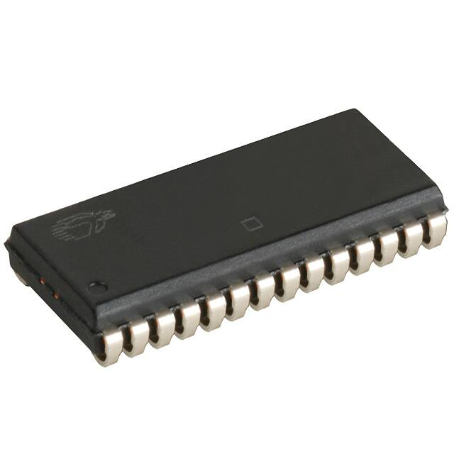
Pin Configuration
DIP/SOJ
Top View
256 x 32 x 9
ARRAY
1
28
V CC
I/O0
A5
2
27
WE
A6
3
26
CE 2
I/O1
A7
4
25
A3
A8
5
24
A2
A9
6
23
A1
A 10
7
22
OE
A 11
8
21
A0
A 12
9
20
CE 1
I/O 0
10
19
I/O 8
I/O 1
11
18
I/O 7
I/O 2
12
17
I/O 6
I/O 3
13
16
I/O 5
GND
14
15
I/O 4
I/O2
SENSE AMPS
A1
A2
A3
A4
A5
A6
A7
A8
ROW DECODER
INPUT BUFFER
A4
I/O3
I/O4
I/O5
I/O6
CE1
CE2
WE
POWER
DOWN
COLUMN
DECODER
I/O8
A12
A11
A10
OE
A0
A9
C182–2
I/O7
C182–1
Selection Guide
7C182-25
7C182-35
7C182-45
Maximum Access Time (ns)
25
35
45
Maximum Operating Current (mA)
140
140
140
Maximum Standby Current (mA)
35
35
35
Cypress Semiconductor Corporation
Document #: 38-05031 Rev. **
•
3901 North First Street
•
San Jose
•
CA 95134 • 408-943-2600
Revised August 24, 2001
�CY7C182
Maximum Ratings
Output Current into Outputs (LOW)............................. 20 mA
Static Discharge Voltage .......................................... >2001V
(per MIL-STD-883, Method 3015.2)
(Above which the useful life may be impaired. For user guidelines, not tested.)
Storage Temperature .....................................−65°C to +150°C
Latch-Up Current.................................................... >200 mA
Ambient Temperature with
Power Applied..................................................−55°C to +125°C
Operating Range
Supply Voltage to Ground Potential[1] ..............−0.5V to +7.0V
Range
Ambient
Temperature
VCC
DC Voltage Applied to Outputs
in High Z State[1] .................................................−0.5V to +7.0V
Commercial
0°C to + 70°C
5V ± 10%
DC Input Voltage[1] ..............................................−0.5V to +7.0V
Electrical Characteristics Over the Operating Range
7C182-25, 35, 45
Parameter
Description
Test Conditions
VOH
Output HIGH Voltage
VCC Min., IOH = −4.0 mA.
VOL
Output LOW Voltage
VCC Min., IOL = 8.0 mA
VIH
Input HIGH Voltage
VIL
Input LOW Voltage[1]
IIX
Input Load Current
GND < VIN < VCC,
GND < VOUT < VCC,
Output Disabled
IOZ
Output Leakage Current
VCC = Max., VOUT = GND
IOS
Output Short Circuit
Current[2]
ICC
Min.
Max.
Unit
2.4
V
0.4
V
2.2
VCC
V
−0.5
0.8
V
−10
+10
µA
−10
+10
µA
VCC = Max., VOUT = GND
−300
mA
VCC Operating Circuit
Current
VCC Max., Output Current = 0 mA,
f = Max., VIN = VCC or GND
140
mA
Automatic Power-Down
Current — TTL Inputs
Max VCC, CE1 > VIH, CE2 < VIL,
VIN > VIH or VIN < VIL, f = fMAX
35
mA
Automatic Power-Down
Current — CMOS Inputs
Max VCC, CE1 > VCC − 0.3V, CE2 < 0.3V,
VIN > VCC − 0.3V or VIN < 0.3V, f = 0
20
mA
Capacitance[3]
Parameter
Description
COUT
Output Capacitance
CIN
Input Capacitance
Test Conditions
TA = 25°C, f = 1 MHz,
VCC = 5.0V
Max.
Unit
10
pF
10
pF
Note:
1. VIL (min.) = −3.0V for pulse durations of less than 20 ns.
2. Duration of the short circuit should not exceed 30 seconds. Not more than one output should be shorted at one time.
3. Tested initially and after any design or process changes that may affect these parameters.
AC Test Loads and Waveforms
R1 481Ω
5V
OUTPUT
R2
255Ω
30 pF
R1 481Ω
5V
OUTPUT
INCLUDING
JIG AND
SCOPE
3.0V
INCLUDING
JIG AND
SCOPE
(a)
Equivalent to:
R2
255Ω
5 pF
C182–3
GND
10%
< 5 ns
ALL INPUT PULSES
90%
90%
10%
< 5 ns
C182–4
(b)
THÉVENIN EQUIVALENT
167Ω
OUTPUT
Document #: 38-05031 Rev. **
1.73V
Page 2 of 7
�CY7C182
Switching Characteristics Over the Operating Range
7C182-25
Parameter
READ CYCLE
Description
Min.
Max.
7C182-35
Min.
Max.
7C182-45
Min.
Max.
Unit
[4]
tRC
Read Cycle Time
tAA
Address to Data Valid
tOHA
Data Hold from Address Change
tACE1
CE1 Access Time
25
35
45
ns
tACE2
CE2 Access Time
25
35
45
ns
tLZCE1
CE1 LOW to Low Z
5
5
5
ns
tLZCE2
CE2 HIGH to Low Z
5
5
5
ns
tHZCE1
25
35
25
3
45
35
3
ns
45
3
ns
[5]
18
20
25
[5]
18
20
25
CE1 HIGH to High Z
ns
ns
tHZCE2
CE2 LOW to High Z
tPU
CE1 LOW to Power-Up
tPD
CE1 HIGH to Power-Down
20
20
25
ns
tDOE
OE Access Time
18
20
20
ns
tLZOE
OE LOW to Low Z
tHZOE
0
0
3
[5]
OE HIGH to High Z
0
3
18
ns
3
20
ns
25
ns
WRITE CYCLE[6]
tWC
Write Cycle Time
25
35
45
ns
tSA
Address Set-Up Time
0
0
0
ns
tAW
Address Valid to End of Write
20
30
40
ns
tSD
Data Set-Up Time
15
20
25
ns
tSCE1
CE1 LOW to Write End
20
30
40
ns
tSCE2
CE2 HIGH to Write End
20
30
40
ns
tPWE
WE Pulse Width
20
25
30
ns
tHA
Address Hold from End of Write
0
0
0
ns
tHD
Data Hold Time
0
0
0
ns
3
3
3
ns
tLZWE
tHZWE
Write HIGH to Low Z
[7]
Write LOW to High Z
[5, 7, 8]
13
15
20
ns
Notes:
4. WE is HIGH for read cycle.
5. tHZCE and tHZWE are specified with CL = 5 pF. Transition is measured ± 500 mV from steady-state voltage.
6. The internal write time of the memory is defined by the overlap of CE1 LOW, CE2 HIGH, and WE LOW. All three signals must be asserted to initiate a write
and any signal can terminate a write by being deasserted. The data input set-up and hold timing should be referenced to the rising edge of the signal that
terminates the write.
7. At any given temperature and voltage condition, tLZWE is less than tHZWE for any given device. These parameters are sampled and not 100% tested.
8. Address valid prior to or coincident with CE transition LOW and CE2 transition HIGH.
Document #: 38-05031 Rev. **
Page 3 of 7
�CY7C182
Switching Waveforms
Read Cycle
No. 1[4, 9]
tRC
ADDRESS
tOHA
DATA OUT
tAA
PREVIOUS DATA VALID
DATA VALID
C182–5
Read Cycle No. 2
[4, 10]
tRC
CE1
tACE1
tACE2
CE2
OE
OE
tHZOE
tDOE
DATA OUT
tHZCE
tLZOE
HIGH IMPEDANCE
HIGH
IMPEDANCE
DATA VALID
tLZCE
VCC
SUPPLY
CURRENT
tPD
tPU
ICC
50%
50%
ISB
C182–6
[6]
Write Cycle No. 1 (WE Controlled)
tWC
ADDRESS
tSCE1
tSCE2
CS1
CS2
tAW
WE
tHA
tSA
tPWE
tHD
tSD
DATA IN
DATA VALID
tHZWE
DATA I/O
tLZWE
HIGH IMPEDANCE
DATA UNDEFINED
C182–7
Notes:
9. Device is continuously selected. OE, CE1 = VIL. CE2 = VIH.
10. If CE1 goes HIGH and CE2 goes LOW simultaneously with WE HIGH, the output remains in a high-impedance state.
Document #: 38-05031 Rev. **
Page 4 of 7
�CY7C182
Switching Waveforms (continued)
Write Cycle No. 2 (CE Controlled)
[6, 10]
tWC
ADDRESS
CE1
tSCE1
tSA
tSCE2
CE2
tHA
tAW
tPWE
WE
tSD
DATA IN
tHD
DATA VALID
tHZWE
HIGH IMPEDANCE
DATA I/O
DATA UNDEFINED
C182–8
Truth Table
CE1
CE2
OE
WE
Data In
Data Out
H
X
X
X
Z
Z
Mode
L
H
L
H
Z
Valid
Read
L
H
X
L
Valid
Z
Write
L
H
H
H
Z
Z
Output Disable
X
L
X
X
Z
Z
Deselect
Deselect/Power-Down
Ordering Information
Speed
(ns)
25
35
45
Ordering Code
Package
Name
Package Type
CY7C182−25PC
P21
28-Lead (300-Mil) Molded DIP
CY7C182−25VC
V21
28-Lead Molded SOJ
CY7C182−35PC
P21
28-Lead (300-Mil) Molded DIP
CY7C182−35VC
V21
28-Lead Molded SOJ
CY7C182−45PC
P21
28-Lead (300-Mil) Molded DIP
CY7C182−45VC
V21
28-Lead Molded SOJ
Document #: 38-05031 Rev. **
Operating
Range
Commercial
Commercial
Commercial
Page 5 of 7
�CY7C182
Package Diagrams
28-Lead (300-Mil) Molded DIP P21
51-85014-B
28-Lead (300-Mil) Molded SOJ V21
51-85031-B
Document #: 38-05031 Rev. **
Page 6 of 7
© Cypress Semiconductor Corporation, 2001. The information contained herein is subject to change without notice. Cypress Semiconductor Corporation assumes no responsibility for the use
of any circuitry other than circuitry embodied in a Cypress Semiconductor product. Nor does it convey or imply any license under patent or other rights. Cypress Semiconductor does not authorize
its products for use as critical components in life-support systems where a malfunction or failure may reasonably be expected to result in significant injury to the user. The inclusion of Cypress
Semiconductor products in life-support systems application implies that the manufacturer assumes all risk of such use and in doing so indemnifies Cypress Semiconductor against all charges.
�CY7C182
Document Title: CY7C182 8K x 9 Static RAM
Document Number: 38-05031
REV.
ECN NO.
Issue
Date
Orig. of
Change
Description of Change
**
106825
09/15/01
SZV
Change from Spec number: 38-00110 to 38-05031
Document #: 38-05031 Rev. **
Page 7 of 7
�


 工商网监
湘ICP备2023018690号
工商网监
湘ICP备2023018690号
