n-Channel Power MOSFET
OptiMOS™
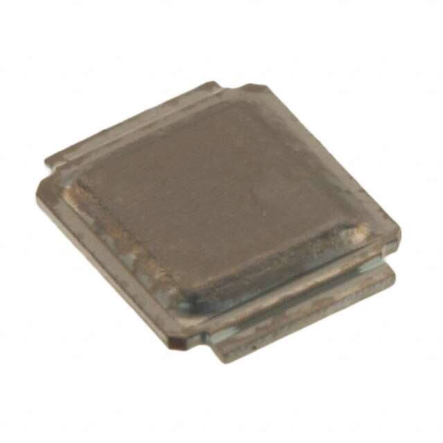
BSB014N04LX3 G
Data Sheet
2.3, 2011-05-24
Final
Industrial & Multimarket
�OptiMOS™ Power-MOSFET
BSB014N04LX3 G
1
Description
OptiMOS™40V products are class leading power MOSFETs for highest power
density and energy efficient solutions. Ultra low gate- and output charges together
with lowest on state resistance in small footprint packages make OptiMOS™ 40V
the best choice forthe demanding requirements of voltage regulator solutions in
Servers, Datacom and Telecom applications. Super fast switching Control FETs
together with low EMI Sync FETs provide solutions that are easy to design in.
OptiMOS™ products are available in high performance packages to tackle your
most challenging applications giving full flexibility in optimizing space- efficiency
and cost. OptiMOS™ products are designed to meet and exceed the energy
efficiency and power density requirements of the sharpened next generation
voltage regulation standards in computing applications
Features
•
•
•
•
•
•
•
•
•
•
•
Optimized for high switching frequency DC/DC converter
100% avalanche tested
Excellent gate charge x RDS(on) product (FOM)
Qualified according to JEDEC1) for target applications
Pb-free plating; RoHS compliant
Very low on-resistance RDS(on)
Low profile (2|ID|RDS(on)max,
ID=30 A
Dynamic characteristics
Parameter
Symbol
Values
Min.
Typ.
Max.
Input capacitance
Ciss
-
12700
16900
Output capacitance
Coss
-
2400
3200
Reverse transfer capacitance
Crss
-
140
-
Turn-on delay time
td(on)
-
12
-
Rise time
tr
-
8.4
-
Turn-off delay time
td(off)
-
60
-
Fall time
tf
-
10
-
Final Data Sheet
3
Unit
Note /
Test Condition
pF
VGS=0 V, VDS=20 V,
f=1 MHz
ns
VDD=20V, VGS=10 V,
ID=30 A, RG= 1.6 Ω
2.3, 2011-05-24
�OptiMOS™ Power-MOSFET
BSB014N04LX3 G
Electrical characteristics
Table 6
Gate charge characteristics1)
Parameter
Symbol
Values
Min.
Typ.
Max.
Unit
Note /
Test Condition
nC
VDD=20 V,
ID=30 A,
VGS=0 to 10 V
Gate to source charge
Qgs
-
33
-
Gate charge at threshold
Qg(th)
-
19
-
Gate to drain charge
Qgd
-
15
-
Switching charge
Qsw
-
29
-
Gate charge total
Qg
-
148
196
Gate plateau voltage
Vplateau
-
2.8
-
V
Gate charge total
Qg
-
71
95
nC
Gate charge total, sync. FET
Qg(sync)
139
VDS=0.1 V,
VGS=0 to 10 V
Output charge
Qoss
89
VDD=20 V, VGS=0 V
VDD=20 V,
ID=30 A,
VGS=0 to 4.5V
1) See figure 16 for gate charge parameter definition
Table 7
Reverse diode characteristics
Parameter
Symbol
Values
Min.
Typ.
Unit
Note /
Test Condition
A
TC=25 °C
Max.
Diode continuous forward current
Is
81
Diode pulse current
IS,pulse
400
Diode forward voltage
VSD
-
0.77
1.1
V
VGS=0 V, IF=30 A,
Tj=25 °C
Reverse recovery charge
Qrr
-
-
50
nC
VR=15 V, IF=Is,
diF/dt=400 A/µs
Final Data Sheet
4
2.3, 2011-05-24
�OptiMOS™ Power-MOSFET
BSB014N04LX3 G
Electrical characteristics diagrams
5
Electrical characteristics diagrams
Table 8
1 Power dissipation
2 Drain current
Ptot = f(TC)
ID=f(TC); parameter:VGS
Table 9
3 Safe operating area TC=25 °C
ID=f(VDS); Tj=25 °C; D=0; parameter: Tp
Final Data Sheet
4 Max. transient thermal impedance
Z(thJC)=f(tp); parameter: D=tp/T
5
2.3, 2011-05-24
�OptiMOS™ Power-MOSFET
BSB014N04LX3 G
Electrical characteristics diagrams
Table 10
5 Typ. output characteristics TC=25 °C
6 Typ. drain-source on-state resistance
ID=f(VDS); Tj=25 °C; parameter: VGS
RDS(on)=f(ID); Tj=25 °C; parameter: VGS
Table 11
7 Typ. transfer characteristics
8 Typ. forward transconductance
ID=f(VGS); |VDS|>2|ID|RDS(on)max
gfs=f(ID); Tj=25 °C
Final Data Sheet
6
2.3, 2011-05-24
�OptiMOS™ Power-MOSFET
BSB014N04LX3 G
Electrical characteristics diagrams
Table 12
9 Drain-source on-state resistance
10 Typ. gate threshold voltage
RDS(on)=f(Tj); ID=30 A; VGS=10 V
VGS(th)=f(Tj); VGS=VDS; ID=250 µA
Table 13
11 Typ. capacitances
12 Forward characteristics of reverse diode
C=f(VDS); VGS=0 V; f=1 MHz
IF=f(VSD); parameter: Tj
Final Data Sheet
7
2.3, 2011-05-24
�OptiMOS™ Power-MOSFET
BSB014N04LX3 G
Electrical characteristics diagrams
Table 14
13 Avalanche characteristics
14 Typ. gate charge
IAS=f(tAV); RGS=25 Ω; parameter: Tj(start)
VGS=f(Qgate); ID=30 A pulsed; parameter: VDD
Table 15
15 Drain-source breakdown voltage
16 Gate charge waveforms
VBR(DSS)=f(Tj); ID=1 mA
Final Data Sheet
8
2.3, 2011-05-24
�OptiMOS™ Power-MOSFET
BSB014N04LX3 G
Package outlines
6
Package outlines
Figure 1
Outlines MG-WDSON-2, dimensions in mm/inches
Final Data Sheet
9
2.3, 2011-05-24
�OptiMOS™ Power-MOSFET
BSB014N04LX3 G
Package outlines
7
Package outlines
Figure 2
Outlines MG-WDSON-2, dimensions in mm/inches
Final Data Sheet
10
2.3, 2011-05-24
�OptiMOS™ Power-MOSFET
BSB014N04LX3 G
Package outlines
8
Package outlines
Figure 3
Outlines MG-WDSON-2, dimensions in mm/inches
9
Marking layout
Final Data Sheet
11
2.3, 2011-05-24
�OptiMOS™ Power-MOSFET
BSB014N04LX3 G
Revision History
9
Revision History
Revision History: 2011-05-24, 2.3
Previous Revision:
Revision
Subjects (major changes since last revision)
0.1
Release of target data sheet
2.2
DirectFET Disclaimer Expired
2.3
Insert Marking Layout
We Listen to Your Comments
Any information within this document that you feel is wrong, unclear or missing at all?
Your feedback will help us to continuously improve the quality of this document.
Please send your proposal (including a reference to this document) to: erratum@infineon.com
Edition 2011-05-24
Published by
Infineon Technologies AG
81726 Munich, Germany
© 2011 Infineon Technologies AG
All Rights Reserved.
Legal Disclaimer
The information given in this document shall in no event be regarded as a guarantee of conditions or
characteristics. With respect to any examples or hints given herein, any typical values stated herein and/or any
information regarding the application of the device, Infineon Technologies hereby disclaims any and all warranties
and liabilities of any kind, including without limitation, warranties of non-infringement of intellectual property rights
of any third party.
Information
For further information on technology, delivery terms and conditions and prices, please contact the nearest
Infineon Technologies Office (www.infineon.com).
Warnings
Due to technical requirements, components may contain dangerous substances. For information on the types in
question, please contact the nearest Infineon Technologies Office.
The Infineon Technologies component described in this Data Sheet may be used in life-support devices or
systems and/or automotive, aviation and aerospace applications or systems only with the express written approval
of Infineon Technologies, if a failure of such components can reasonably be expected to cause the failure of that
life-support, automotive, aviation and aerospace device or system or to affect the safety or effectiveness of that
device or system. Life support devices or systems are intended to be implanted in the human body or to support
and/or maintain and sustain and/or protect human life. If they fail, it is reasonable to assume that the health of the
user or other persons may be endangered.
Final Data Sheet
12
2.3, 2011-05-24
�


 工商网监
湘ICP备2023018690号
工商网监
湘ICP备2023018690号
