TLF1963
Low Dropout Linear Voltage Post Regulator
TLF1963TB
TLF1963TE
Data Sheet
Rev. 1.0, 2012-11-08
Automotive Power
�TLF1963
Table of Contents
Table of Contents
1
Overview . . . . . . . . . . . . . . . . . . . . . . . . . . . . . . . . . . . . . . . . . . . . . . . . . . . . . . . . . . . . . . . . . . . . . . . 3
2
Block Diagram . . . . . . . . . . . . . . . . . . . . . . . . . . . . . . . . . . . . . . . . . . . . . . . . . . . . . . . . . . . . . . . . . . . 4
3
3.1
3.2
3.3
3.4
Pin Configuration . . . . . . . . . . . . . . . . . . . . . . . . . . . . . . . . . . . . . . . . . . . . . . . . . . . . . . . . . . . . . . . .
Pin Assignment TLF1963TB . . . . . . . . . . . . . . . . . . . . . . . . . . . . . . . . . . . . . . . . . . . . . . . . . . . . . . . . .
Pin Definitions and Functions TLF1963TB . . . . . . . . . . . . . . . . . . . . . . . . . . . . . . . . . . . . . . . . . . . . . .
Pin Assignment TLF1963TE . . . . . . . . . . . . . . . . . . . . . . . . . . . . . . . . . . . . . . . . . . . . . . . . . . . . . . . . .
Pin Definitions and Functions TLF1963TE . . . . . . . . . . . . . . . . . . . . . . . . . . . . . . . . . . . . . . . . . . . . . .
5
5
5
6
6
4
4.1
4.2
4.3
General Product Characteristics . . . . . . . . . . . . . . . . . . . . . . . . . . . . . . . . . . . . . . . . . . . . . . . . . . . .
Absolute Maximum Ratings . . . . . . . . . . . . . . . . . . . . . . . . . . . . . . . . . . . . . . . . . . . . . . . . . . . . . . . . .
Functional Range . . . . . . . . . . . . . . . . . . . . . . . . . . . . . . . . . . . . . . . . . . . . . . . . . . . . . . . . . . . . . . . . .
Thermal Resistance . . . . . . . . . . . . . . . . . . . . . . . . . . . . . . . . . . . . . . . . . . . . . . . . . . . . . . . . . . . . . . .
7
7
8
8
5
5.1
5.2
Electrical Characteristics . . . . . . . . . . . . . . . . . . . . . . . . . . . . . . . . . . . . . . . . . . . . . . . . . . . . . . . . . . 9
Electrical Characteristics Voltage Regulator . . . . . . . . . . . . . . . . . . . . . . . . . . . . . . . . . . . . . . . . . . . . . 9
Typical Performance Characteristics . . . . . . . . . . . . . . . . . . . . . . . . . . . . . . . . . . . . . . . . . . . . . . . . . 11
6
6.1
6.2
6.3
6.4
6.5
6.6
Application Information . . . . . . . . . . . . . . . . . . . . . . . . . . . . . . . . . . . . . . . . . . . . . . . . . . . . . . . . . .
Adjustable Operation . . . . . . . . . . . . . . . . . . . . . . . . . . . . . . . . . . . . . . . . . . . . . . . . . . . . . . . . . . . . .
Output Capacitance and Transient Response . . . . . . . . . . . . . . . . . . . . . . . . . . . . . . . . . . . . . . . . . .
Overload Recovery . . . . . . . . . . . . . . . . . . . . . . . . . . . . . . . . . . . . . . . . . . . . . . . . . . . . . . . . . . . . . . .
Output Voltage Noise . . . . . . . . . . . . . . . . . . . . . . . . . . . . . . . . . . . . . . . . . . . . . . . . . . . . . . . . . . . . .
Protection Features . . . . . . . . . . . . . . . . . . . . . . . . . . . . . . . . . . . . . . . . . . . . . . . . . . . . . . . . . . . . . .
Further Application Information . . . . . . . . . . . . . . . . . . . . . . . . . . . . . . . . . . . . . . . . . . . . . . . . . . . . . .
7
Package Outlines . . . . . . . . . . . . . . . . . . . . . . . . . . . . . . . . . . . . . . . . . . . . . . . . . . . . . . . . . . . . . . . 21
8
Revision History . . . . . . . . . . . . . . . . . . . . . . . . . . . . . . . . . . . . . . . . . . . . . . . . . . . . . . . . . . . . . . . . 23
Data Sheet
2
18
18
19
19
19
19
20
Rev. 1.0, 2012-11-08
�Low Dropout Linear Voltage Post Regulator
1
TLF1963
Overview
Features
•
•
•
•
•
•
•
•
•
•
•
•
•
•
•
•
Adjustable Output Voltage
Output Voltage Tolerance at small loads of ±1.5 %
Output Current Capability up to 1.5 A
Very Low Dropout Voltage of 340 mV
Extended Operating Range Starting at 1.7 V
Low Noise of typ. 40 µVRMS (10 Hz to 100 kHz)
Small Output Capacitor for Stability 10 µF
Suitable for Ceramic Output Capacitors
Enable Functionality
Overtemperature Shutdown
Reverse Polarity Protection
Output Current Limitation
Wide Temperature Range From -40 °C up to 150 °C
Suitable for use in automotive electronics as Post Regulator
Green Product (RoHS compliant)
AEC Qualified
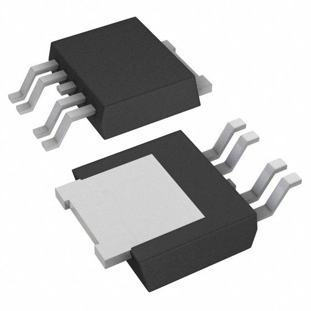
PG-TO263-5
Functional Description
TLF1963 is a low dropout voltage regulator available in PG-TO263-5 and
PG-TO252-5
PG-TO252-5 SMD package. The IC regulates an input voltage VI in the
range of 2.5 V < VI < 20 V to an adjustable output voltage of
1.21 V < VQ,nom < VI -Vdr. The device is capable to supply loads up to 1.5 A. The regulator can be enabled and
disabled via the Enable input. The integrated output current limitation and the overtemperature shutdown will
protect the device against failures like output short circuit to GND, overcurrent and overtemperature.
The TLF1963 provides the ideal solution for systems requiring several supply voltages. With its adjust feature the
regulator can provide all supply voltages between 1.21 V and the available input voltage, this offers a high flexibility
to the system designer.
Choosing External Components
The input capacitor CI is necessary for compensating line influences. The output capacitor CQ is necessary for the
stability of the regulating circuit. Stability is guaranteed at values specified in “Functional Range” on Page 8
within the whole operating temperature range.
Type
Package
Marking
TLF1963TB
PG-TO263-5
T1963V
TLF1963TE
PG-TO252-5
T1963V
Data Sheet
3
Rev. 1.0, 2012-11-08
�TLF1963
Block Diagram
2
Block Diagram
TLF1963 ADJ
IN
Reverse Polarity
Protection
4 Q
2
EN 4
Bias
Voltage
reference
Saturation
Control
Over Current
Protection
Temperature
Protection
Error
Amplifier
5 ADJ
3
GND
Figure 1
Data Sheet
Block Diagram
4
Rev. 1.0, 2012-11-08
�TLF1963
Pin Configuration
3
Pin Configuration
3.1
Pin Assignment TLF1963TB
GND
1
5
GND
EN
I
ADJ
Q
Figure 2
Pin Configuration PG-TO263-5
3.2
Pin Definitions and Functions TLF1963TB
Pin
Symbol
Function
1
EN
Enable;
A low signal disables the IC. A high signal switches it on.
Connect to the input I, if enable functionality is not required.
2
I
Input voltage;
IC supply. For compensating line influences, a capacitor close to the IC pins is recommended.
3
GND
Ground
4
Q
Output voltage;
Connect a capacitor between Q and GND close to the IC terminals, respecting the values
given for its capacitance CQ and ESR given in the table “Functional Range” on Page 8
5
ADJ
Adjust Input;
Connect an external voltage divider from Q to GND to determine the output voltage.
By connecting the output pin Q directly to the adjust pin ADJ without resistors an ouput
voltage equal to the reference voltage VADJ = 1.21 V is determined.
TAB
GND
Ground
Data Sheet
5
Rev. 1.0, 2012-11-08
�TLF1963
Pin Configuration
3.3
Pin Assignment TLF1963TE
GND
1
5
EN
ADJ
Q
I
Figure 3
Pin Configuration PG-TO252-5
3.4
Pin Definitions and Functions TLF1963TE
Pin
Symbol
Function
1
EN
Enable;
A low signal disables the IC. A high signal switches it on.
Connect to the input I, if enable functionality is not required.
2
I
Input voltage;
IC supply. For compensating line influences, a capacitor close to the IC pins is recommended.
3
GND
Ground
4
Q
Output voltage;
Connect a capacitor between Q and GND close to the IC terminals, respecting the values
given for its capacitance CQ and ESR given in the table “Functional Range” on Page 8
5
ADJ
Adjust Input;
Connect an external voltage divider from Q to GND to determine the output voltage.
By connecting the output pin Q directly to the adjust pin ADJ without resistors an ouput
voltage equal to the reference voltage VADJ = 1.21 V is determined.
TAB
GND
Ground
Data Sheet
6
Rev. 1.0, 2012-11-08
�TLF1963
General Product Characteristics
4
General Product Characteristics
4.1
Absolute Maximum Ratings
Table 1
Absolute Maximum Ratings 1)
Tj = -40 °C to +150 °C; all voltages with respect to ground (unless otherwise specified)
Pos.
Parameter
Symbol
Limit Values
Min.
Max.
Unit
Conditions
Input, Enable
4.1.1
Voltage
VI, VEN
-20
20
V
–
Voltage
VADJ
-7
7
V
–
Voltage
VQ
-20
20
V
–
Tj
Tstg
-40
150
°C
–
-50
150
°C
–
VESD
VESD
-2
2
kV
HBM2)
-750
750
V
CDM3)
Adjust
4.1.2
Output
4.1.3
Temperatures
4.1.4
Junction Temperature
4.1.5
Storage Temperature
ESD Susceptibility
4.1.6
ESD Resistivity
4.1.7
ESD Resistivity
1) Not subject to production test, specified by design.
2) ESD HBM Test according AEC-Q100-002 - JESD22-A114 (1.5 kOhm, 100 pF)
3) ESD susceptibility, Charged Device Model “CDM” EIA/JESD22-C101 or ESDA STM5.3.1
Note: Stresses above the ones listed here may cause permanent damage to the device. Exposure to absolute
maximum rating conditions for extended periods may affect device reliability.
Note: Integrated protection functions are designed to prevent IC destruction under fault conditions described in the
data sheet. Fault conditions are considered as “outside” normal operating range. Protection functions are
not designed for continuous repetitive operation.
Data Sheet
7
Rev. 1.0, 2012-11-08
�TLF1963
General Product Characteristics
4.2
Functional Range
Table 2
Functional Range
Pos.
Parameter
4.2.1
Input voltage
4.2.2
Output Capacitor’s Requirements
for Stability
4.2.3
Junction temperature
Symbol
VI
CQ
ESR(CQ)
Tj
Limit Values
Unit
Conditions
Min.
Max.
2.5
20
V
–
10
–
µF
–1)
–
3
Ω
–2)
-40
150
°C
1) the minimum output capacitance requirement is applicable for a worst case capacitance tolerance of 30%
2) relevant ESR value at f = 10 kHz
Note: Within the functional or operating range, the IC operates as described in the circuit description. The electrical
characteristics are specified within the conditions given in the Electrical Characteristics table.
4.3
Thermal Resistance
Note: This thermal data was generated in accordance with JEDEC JESD51 standards. For more information, go
to www.jedec.org.
Table 3
Pos.
Thermal Resistance
Parameter
Symbol
Limit Values
Min.
Typ.
Max.
Unit
Conditions
Package PG-TO263-5
4.3.1
Junction to Case1)
RthJC
–
0.84
–
K/W
measured to heat
slug
4.3.2
Junction to Ambient1)
RthJA
–
19
–
K/W
2)
4.3.3
–
64
–
K/W
footprint only3)
4.3.4
–
36
–
K/W
300 mm² heatsink
area3)
4.3.5
–
29
–
K/W
600 mm² heatsink
area3)
Package PG-TO252-5
4.3.6
Junction to Case1)
RthJC
–
0.78
–
K/W
measured to heat
slug
4.3.7
Junction to Ambient1)
RthJA
–
24
–
K/W
2)
4.3.8
–
95
–
K/W
footprint only3)
4.3.9
–
50
–
K/W
300 mm² heatsink
area3)
4.3.10
–
38
–
K/W
600 mm² heatsink
area3)
1) Not subject to production test, specified by design.
2) Specified RthJA value is according to Jedec JESD51-2,-5,-7 at natural convection on FR4 2s2p board; The Product
(Chip+Package) was simulated on a 76.2 x 114.3 x 1.5 mm³ board with 2 inner copper layers (2 x 70 µm Cu, 2 x 35 µm Cu).
Where applicable a thermal via array under the exposed pad contacted the first inner copper layer.
3) Specified RthJA value is according to Jedec JESD 51-3 at natural convection on FR4 1s0p board; The Product
(Chip+Package) was simulated on a 76.2 × 114.3 × 1.5 mm3 board with 1 copper layer (1 x 70 µm Cu).
Data Sheet
8
Rev. 1.0, 2012-11-08
�TLF1963
Electrical Characteristics
5
Electrical Characteristics
5.1
Electrical Characteristics Voltage Regulator
Table 4
Electrical Characteristics:
VI = 2.5 V - 20 V, Tj = -40 °C to +150 °C, all voltages with respect to ground, positive current flowing out of the pin
(unless otherwise specified)
Pos.
5.1.1
Parameter
Symbol
Min.
Typ.
Max.
Min. Input Voltage 1) 2)
VI,min
VI,min
VADJ
–
1.7
–
2.1
5.1.2
5.1.3
Adjustable Pin Voltage
1) 3)
5.1.4
Limit Values
1.192 1.21
Unit
Conditions
–
V
2.5
V
IQ = 0.5 A; Tj = 25 °C
IQ = 1.5 A
VI = 2.21 to 20 V;
IQ = 1 mA;
Tj = 25 °C
IQ = 1 mA to 1.5 A
VI = 2.21 to 20 V;
IQ = 1 mA
IQ = 1 mA to 1.5 A;
VI = 2.5 V; Tj = 25 °C
IQ = 1 mA to 1.5 A;
VI = 2.5 V
IQ = 1 mA; Tj = 25 °C
IQ = 1 mA
IQ = 100 mA;
Tj = 25 °C
IQ = 100 mA
IQ = 500 mA;
Tj = 25 °C
IQ = 500 mA
IQ = 1.5 A;
Tj = 25 °C
IQ = 1.5 A
IQ = 0 mA
IQ = 1 mA
IQ = 100 mA
IQ = 500 mA
IQ = 1.5 A
CQ = 10 µF; IQ = 1.5 A;
1.228 V
1.174 1.21
1.246 V
5.1.5
Line regulation 1)
ΔVQ,line
–
1.0
3
mV
5.1.6
Load regulation 1)
ΔVQ,load
–
2
8
mV
–
–
12
mV
–
0.01
0.03
V
–
–
0.04
V
5.1.10
–
0.03
0.05
V
5.1.11
–
–
0.09
V
5.1.12
–
0.13
0.25
V
5.1.13
–
–
0.27
V
5.1.14
–
0.34
0.45
V
–
–
0.55
V
–
1.0
1.5
mA
–
1.1
1.7
mA
5.1.18
–
3.8
5.0
mA
5.1.19
–
15
22
mA
5.1.20
–
80
130
mA
–
40
–
µVRMS
5.1.7
5.1.8
5.1.9
Dropout voltage 2) 4) 5)
VI = VQ,nom
Vdr
5.1.15
5.1.16
GND Pin Current
5.1.17
VI = VQ,nom + 1 V
5.1.21
4) 6)
Iq
VQ,noise
Output Voltage Noise
BW = 10 Hz to 100 kHz
5.1.22
ADJ Pin Bias Current
5.1.23
Enable Threshold
5.1.24
5.1.25
EN Pin current
5.1.26
Data Sheet
8)
1) 7)
IADJ
–
1
2
µA
–
VEN,LH
VEN,HL
IEN
–
1.4
2
V
0.8
1.3
–
V
–
0
0.2
µA
–
2.5
20
µA
VQ = Off to On
VQ = On to Off
VEN = 0 V
VEN ≤ 20 V
9
Rev. 1.0, 2012-11-08
�TLF1963
Electrical Characteristics
Table 4
Electrical Characteristics: (cont’d)
VI = 2.5 V - 20 V, Tj = -40 °C to +150 °C, all voltages with respect to ground, positive current flowing out of the pin
(unless otherwise specified)
Pos.
Parameter
Symbol
Unit
Conditions
VI = 6 V; VEN = 0 V;
Tj ≤ 85 °C
Tj = 25 °C;
fr = 120 Hz;
IQ = 0.75 A;
VI - VQ = 1.5 V;
Vr = 0.5 Vpp
Tj = 25 °C;
VI = 7 V; VQ = 0 V
VI = VQ,nom + 1 V;
dVQ = -0.1 V
VI = -20 V;
VQ = 0 V
Tj = 25 °C;
VQ = 1.21 V;
VI < 1.21 V
VQ = 1.21 V;
VI < 1.21 V
Min.
Typ.
Max.
–
0.01
1
µA
55
67
–
dB
IQ
–
2
–
A
IQ
1.6
–
–
A
Iq,off
5.1.27
Quiescent Current in
Shutdown 9)
5.1.28
Power Supply ripple rejection 10) PSRR
5.1.29
Output current limitation
5.1.30
Limit Values
5.1.31
Input Reverse Leakage Current II,rev
–
–
2
mA
5.1.32
Reverse Output Current 11)
–
300
600
µA
–
–
1
mA
5.1.33
IQ,rev
1)
2)
The TLF1963 is tested and specified for these conditions with the ADJ pin connected to the Q pin.
For TLF1963 dropout voltage will be limited by the minimum input voltage specification under some output voltage/load
conditions.
3) Operating conditions are limited by maximum junction temperature. The regulated output voltage specification will not apply
for all possible combinations of input voltage and output current. When operating at maximum input voltage, the output
current range must be limited. When operating at maximum output current, the input voltage range must be limited.
4) To satisfy requirements for minimum input voltage, the TLF1963 is tested and specified for these conditions with an
external resistor divider (two 4.12 kΩ resistors) for an output voltage of 2.4 V. The external resistor divider will add a 300 µA
DC load on the output.
5) Dropout voltage is the minimum input to output voltage differential needed to maintain regulation at a specified output
current. In dropout, the output voltage will be equal to: VI – Vdr
6) GND pin current is tested with VI = VQ,nom + 1 V and a current source load.
7) ADJ pin bias current flows into the ADJ pin.
8) EN pin current flows into the EN pin.
9) Specified by design, tested at Tamb = 25 °C
10) Not subject to production test, specified by design.
11) Reverse output current is tested with the IN pin grounded and the Q pin forced to the rated output voltage. This current
flows into the Q pin and out the GND pin
Data Sheet
10
Rev. 1.0, 2012-11-08
�TLF1963
Electrical Characteristics
5.2
Typical Performance Characteristics
Dropout Voltage VDR versus
Output Current IQ
Guaranteed Dropout Voltage Vdr versus
Output Current IQ
550
550
500
500
450
450
400
400
350
350
Vdr [mV]
Vdr [mV]
Δ : Testpoint
300
250
200
300
250
200
150
150
Tj = −40 °C
100
Tj = 25 °C
100
50
Tj = 125 °C
50
Tj = 25 °C
Tj = 150 °C
0
0
0.5
1
Tj = 150 °C
0
1.5
0
0.5
IQ [A]
Dropout Voltage Vdr versus
Temperature Tj
450
1.5
Quiescent Current Iq versus
Temperature Tj
550
500
1
IQ [A]
2
IQ = 100 mA
1.8
IQ = 500 mA
IQ = 1.5 A
1.6
400
1.4
350
Iq [mA]
Vdr [mV]
1.2
300
250
1
0.8
200
0.6
150
0.4
100
0
−50
Data Sheet
VI = 6 V
IQ = 0 mA .
VEN = VI
0.2
50
0
50
Tj [°C]
100
0
−50
150
11
0
50
Tj [°C]
100
150
Rev. 1.0, 2012-11-08
�TLF1963
Electrical Characteristics
Adjustable Voltage VADJ versus
Temperature Tj
Quiescent Current Iq versus
Input Voltage VI (VQ,nom = 2.5 V)
1.22
25
VQ,nom = 2.5 V
Tj = 25 °C
IQ = 0 mA
1.215
20
1.21
Iq [mA]
VADJ [V]
15
1.205
10
1.2
IQ = 1 mA
1.195
5
IQ = 100 mA
IQ = 500 mA
IQ = 1.5 A
1.19
−50
0
50
Tj [°C]
100
0
150
0
4
6
8
10
VI [V]
Quiescent Current Iq versus
Input Voltage VI (VQ,nom = 1.21 V)
GND Pin Current IGND versus
Output Current IQ
1.8
120
VQ,nom = 1.21 V
Tj = 25 °C
IQ = 0 mA
1.6
Tj = −40 °C
Tj = 25 °C
Tj = 125 °C
100
1.4
Tj = 150 °C
1.2
80
IGND [mA]
Iq [mA]
2
1
0.8
0.6
60
40
0.4
20
0.2
VI = VQ,nom + 1 V
0
0
2
4
6
8
0
10
VI [V]
Data Sheet
0
0.5
1
1.5
IQ [A]
12
Rev. 1.0, 2012-11-08
�TLF1963
Electrical Characteristics
GND Pin Current IGND versus
Input Voltage VI (VQ,nom = 2.5 V)
GND Pin Current IGND versus
Input Voltage VI (VQ,nom = 1.21 V)
30
IQ = 1 mA
IQ = 1 mA
IQ = 100 mA
IQ = 100 mA
25
IQ = 500 mA
25
IQ = 500 mA
20
VQ,nom = 2.5 V
Tj = 25 °C
20
VQ,nom = 1.21 V
Tj = 25 °C
IGND [mA]
IGND [mA]
30
15
15
10
10
5
5
0
0
2
4
6
8
0
10
0
2
4
VI [V]
GND Pin Current IGND versus
Input Voltage VI (VQ,nom = 2.5 V)
10
100
VQ,nom = 2.5 V
Tj = 25 °C
90
80
70
70
60
IQ = 100 mA
40
IQ = 1.5 A
IGND [mA]
IQ = 1 mA
50
IQ = 500 mA
IQ = 100 mA
40
IQ = 1.5 A
30
20
20
10
10
2
4
6
8
0
10
VI [V]
Data Sheet
IQ = 1 mA
50
30
0
VQ,nom = 1.21 V
Tj = 25 °C
90
80
60
IGND [mA]
8
GND Pin Current IGND versus
Input Voltage VI (VQ,nom = 1.21 V)
100
0
6
VI [V]
IQ = 500 mA
0
2
4
6
8
10
VI [V]
13
Rev. 1.0, 2012-11-08
�TLF1963
Electrical Characteristics
EN Pin Thresholds VEN,th versus
Temperature Tj
EN Pin Input Current IEN versus
EN Pin Voltage VEN
2
3.5
Threshold Off−to−On
Threshold On−to−Off
3
1.8
2.5
IEN [µA]
VEN,th [V]
1.6
1.4
2
1.5
1.2
1
1
0.8
−50
Tj = 25 °C
VI = 20 V
0.5
0
50
Tj [°C]
100
0
150
EN Pin Input Current IEN versus
Temperature Tj
0
5
10
VEN [V]
15
20
Adjustable Pin Bias Current IADJ versus
Temperature Tj
1.2
5
4.5
1
4
3.5
0.8
IADJ [µA]
IEN [µA]
3
2.5
0.6
2
0.4
1.5
1
0.2
0.5
VEN = 20 V .
0
−50
Data Sheet
0
50
Tj [°C]
100
0
−50
150
14
0
50
Tj [°C]
100
150
Rev. 1.0, 2012-11-08
�TLF1963
Electrical Characteristics
Current Limit IQ,max versus
Input / Output Differential VIN - VQ
Current Limit IQ,max versus
Temperature Tj
3
3.5
ΔVQ = −100 mV .
VI = 7 V
VQ = 0 V .
3
2.5
2.5
IQ,max [A]
IQ,max [A]
2
1.5
2
1.5
1
1
Tj = −40 °C
Tj = 25 °C
0.5
0.5
Tj = 125 °C
Tj = 150 °C
0
0
5
10
VIN − VQ [V]
15
0
−50
20
Reverse Output Current IQ,rev versus
Output Voltage VQ
50
Tj [°C]
150
1
VI = 0 V
4.5 Tj = 25 °C .
0.9
0.8
3.5
0.7
3
0.6
IQ,rev [mA]
4
2.5
0.5
2
0.4
1.5
0.3
1
0.2
VQ.nom = 1.21 V
0.5
0.1
VIN = 0 V
VQ = 1.21 V .
VQ.nom = 2.5 V
0
100
Reverse Output Current IQ,rev versus
Temperature Tj
5
IQ,rev [mA]
0
0
2
4
6
8
0
−50
10
VQ [V]
Data Sheet
15
0
50
Tj [°C]
100
150
Rev. 1.0, 2012-11-08
�TLF1963
Electrical Characteristics
Ripple Rejection PSRR versus
Frequency f
Ripple Rejection PSRR versus
Temperature Tj
70
80
IL = 0.75 A
VI = VQnom + 1 V
Tj = 25 °C
CQ = 10 µF Ceramic .
70
68
66
60
64
PSRR [dB]
PSRR [dB]
50
40
62
60
30
58
20
56
IL = 0.75 A
VI = VQ,nom + 1 V .
fRipple = 120 Hz
10
54
0
10
100
1k
10k
100k
−50
1M
0
f [Hz]
3
10
2.5
8
2
6
1.5
1
4
0
IQ = 1 mA
dILoad = 1 mA to 1.5 A .
VI = 2.7 V
VQ,nom = 1.21 V
IQ = 500 mA
IQ = 1.5 A
Data Sheet
150
2
0.5
0
−50
100
Load Regulation dVLoad versus
Temperature Tj
dVLoad [mV]
VI,min [V]
Minimum Input Voltage VI,min versus
Temperature Tj
50
Tj [°C]
0
50
Tj [°C]
100
−2
−50
150
16
0
50
Tj [°C]
100
150
Rev. 1.0, 2012-11-08
�TLF1963
Electrical Characteristics
Equivalent Series Resistance ESR(CQ) vs
Load Current IQ
10
Max ESR
Min ESR
9
8
ESR(CQ) [Ω]
7
6
5
4
3
2
CQ = 10 µF .
1
0
1m
10m
100m
1
IQ [A]
Data Sheet
17
Rev. 1.0, 2012-11-08
�TLF1963
Application Information
6
Application Information
Note: The following information is given as a hint for the implementation of the device only and shall not be
regarded as a description or warranty of a certain functionality, condition or quality of the device.
The TLF1963 is an 1.5 A low dropout regulator optimized for fast transient response. The device is capable of
supplying 1.5 A at a very low dropout voltage up to a Junction Temperature of 150 °C. The low operating quiescent
current of 1 mA drops to less than 1 µA in case the device is disabled. In addition to the low quiescent current, the
TLF1963 incorporates several protection features which make them ideal for use in battery-powered systems. The
device is protected against both reverse input and reverse output voltages.
Note: This is a very simplified example of an application circuit. The function must be verified in the real application.
VBat
2
TLF1963
VQ
Q 4
I
10µF
R2
ADJ
10 µF
5
R1
EN
1
GND
3
Figure 4
Application Diagram
6.1
Adjustable Operation
The TLF1963 has an output voltage range of 1.21 V to VI - Vdr < 20 V. The output voltage is set by the ratio of two
external resistors as shown in Figure 4. The device serves the output to maintain the voltage at the ADJ pin at
1.21 V referenced to ground. The current in R1 is then equal to 1.21 V / R1 and the current in R2 is the current in
R1 plus the ADJ pin bias current. The ADJ pin bias current, 1 µA at 25 °C, flows through R2 into the ADJ pin. The
output voltage can be calculated using the formula in Equation (1).
R
V Q = V ADJ ⋅ ⎛ 1 + -----2-⎞ + I ADJ ⋅ R 2
⎝
R ⎠
(1)
1
VADJ = 1.21 V typical
IADJ = 1 µA at 25 °C
The value of R1 is recommended to be smaller than 12 kΩ to minimize errors in the output voltage caused by the
ADJ pin bias current. Note that in shutdown the output is turned off and the divider current will be zero.
The adjustable device is mainly tested and specified with the ADJ pin connected to the Q pin for an output voltage
of 1.21 V. Specifications for output voltages adjusted to greater values than 1.21V will be proportional to the ratio
of the desired output voltage to 1.21 V.
For example, load regulation for an output current change of 1 mA to 1.5 A is ΔVQ,load = 2 mV typical at
VQ,nom = 1.21 V.
At VQ,nom = 5 V, load regulation is: ΔVQ,load,5V = (5 V / 1.21 V)•(2 mV) = 8.3 mV
Data Sheet
18
Rev. 1.0, 2012-11-08
�TLF1963
Application Information
6.2
Output Capacitance and Transient Response
The TLF1963 is designed to be stable with a wide range of output capacitors. The ESR of the output capacitor
affects stability, most notably with small capacitors. A minimum output capacitor of 10 µF with an ESR in the range
of 10 mΩ to 3 Ω is recommended to prevent oscillations. Larger values of output capacitance can decrease the
peak deviations and provide improved transient response for larger load current changes.
6.3
Overload Recovery
The TLF1963 has a safe operating area protection. The device protects itself by limiting the output current to a
maximum and prevent it self against destruction due to overload or short circuits conditions. In this cases the
current is limited and the resulting output voltage decreases according to the load down to 0V in a short circuit
condition.
The TLF1963 can supply the application for all input voltages between 2.5 V up to 20V with currents up to 1.5 A.
Of course it needs to be ensured, that the junction temperature stays within the operating range up to 150 °C. For
startup conditions with a high load current the TLF1963 is able to start up properly without exeeding the safe
operating area. Even imediatly after removal of a short circuit failure case the device is able to start if the load
current is very high. The characteristic of the current limitation can by seen in the typical perfomance graphs on
Page 15.
6.4
Output Voltage Noise
The TLF1963 has been designed to provide low output voltage noise over the 10 Hz to 100 kHz bandwidth while
operating at full load. Output voltage noise is typically 40 µVRMS over this frequency bandwidth. For higher output
voltages (generated by using a resistor divider), the output voltage noise will be gained up accordingly.
Higher values of output voltage noise may be measured when care is not exercised with regards to circuit layout
and testing. Crosstalk from nearby traces can induce unwanted noise onto the output of the TLF1963. Power
supply ripple rejection must also be considered, because the TLF1963 does not have unlimited power supply
ripple rejection and will pass a small portion of the input noise through to the output.
6.5
Protection Features
The TLF1963 has several protection features which makes him ideal for use in battery-powered circuits. In addition
to the normal protection features associated with monolithic regulators, such as current limiting and thermal
limiting, the device is protected against reverse input voltages and reverse output voltages.
Current limit protection and thermal overload protection are intended to protect the device against current overload
conditions at the output of the device. For normal operation, the junction temperature should not exceed 150 °C.
The input of the device will withstand reverse voltages of 20 V. Current flow out of the device will be limited to less
than 2 mA in case of an input voltage of -20 V at the Input and no negative voltage will appear at the output. The
device will protect both itself and the load. This provides protection against batteries that can be plugged in
backward.
The output of the TLF1963 can be pulled below ground without damaging the device. If the input is left open circuit
or grounded, the output can be pulled below ground by 20 V. The output will act like an open circuit, no current
will flow out of the pin. If the input is powered by a voltage source, the output will source the short-circuit current
of the device and will protect itself by thermal limiting. In this case, grounding the EN pin will turn off the device
and stop the output from sourcing the short-circuit current.
The ADJ pin of the adjustable device can be pulled above or below ground by as much as 7 V without damaging
the device. If the input is left open circuit or grounded, the ADJ pin will act like an open circuit when pulled below
ground and like a resistor (typically 4 kΩ) in series with a diode when pulled above ground.
In situations where the ADJ pin is connected to a resistor divider that would pull the ADJ pin above its 7 V clamp
voltage if the output is pulled high, the ADJ pin input current must be limited to less than 5 mA. For example, a
resistor divider is used to provide a regulated 1.5V output from the 1.21 V reference when the output is forced to
Data Sheet
19
Rev. 1.0, 2012-11-08
�TLF1963
Application Information
20 V. The top resistor of the resistor divider must be chosen to limit the current into the ADJ pin to less than 5 mA
when the ADJ pin is at 7 V. The 13 V difference between Q and ADJ pins divided by the 5 mA maximum current
into the ADJ pin yields a minimum top resistor value of 2.6 kΩ.
6.6
•
Further Application Information
For further information you may contact http://www.infineon.com/
Data Sheet
20
Rev. 1.0, 2012-11-08
�TLF1963
Package Outlines
7
Package Outlines
4.4
10 ±0.2
1.27 ±0.1
A
8.5 1)
B
0.05
2.4
0.1
2.7 ±0.3
4.7 ±0.5
7.55 1)
9.25 ±0.2
(15)
1±0.3
0...0.3
0...0.15
5 x 0.8 ±0.1
0.5 ±0.1
4 x 1.7
0.25
M
A B
8˚ MAX.
1) Typical
Metal surface min. X = 7.25, Y = 6.9
All metal surfaces tin plated, except area of cut.
Figure 5
Data Sheet
0.1 B
GPT09113
PG-TO263-5 SMD Package
21
Rev. 1.0, 2012-11-08
�TLF1963
Package Outlines
A
5.7 MAX. 1)
B
0.5 +0.08
-0.04
0.9 +0.20
-0.01
0...0.15
0.51 MIN.
9.98 ±0.5
6.22 -0.2
0.15 MAX.
per side
5 x 0.6 ±0.1
1.14
4.56
0.5 +0.08
-0.04
0.1 B
0.25
M
A B
1) Includes mold flashes on each side.
All metal surfaces tin plated, except area of cut.
Figure 6
2.3 +0.05
-0.10
(5)
0.8 ±0.15
1±0.1
(4.24)
6.5 +0.15
-0.05
PG-TO252-5-13-PO V0.1
PG-TO252-5 SMD Package
Green Product (RoHS compliant)
To meet the world-wide customer requirements for environmentally friendly products and to be compliant with
government regulations the device is available as a green product. Green products are RoHS-Compliant (i.e
Pb-free finish on leads and suitable for Pb-free soldering according to IPC/JEDEC J-STD-020).
For further information on alternative packages, please visit our website:
http://www.infineon.com/packages.
Data Sheet
22
Dimensions in mm
Rev. 1.0, 2012-11-08
�TLF1963
Revision History
8
Revision History
Revision
Date
Changes
1.0
2012-11-08
Initial Version of Data Sheet
Data Sheet
23
Rev. 1.0, 2012-11-08
�Edition 2012-11-08
Published by
Infineon Technologies AG
81726 Munich, Germany
© 2012 Infineon Technologies AG
All Rights Reserved.
Legal Disclaimer
The information given in this document shall in no event be regarded as a guarantee of conditions or
characteristics. With respect to any examples or hints given herein, any typical values stated herein and/or any
information regarding the application of the device, Infineon Technologies hereby disclaims any and all warranties
and liabilities of any kind, including without limitation, warranties of non-infringement of intellectual property rights
of any third party.
Information
For further information on technology, delivery terms and conditions and prices, please contact the nearest
Infineon Technologies Office (www.infineon.com).
Warnings
Due to technical requirements, components may contain dangerous substances. For information on the types in
question, please contact the nearest Infineon Technologies Office.
Infineon Technologies components may be used in life-support devices or systems only with the express written
approval of Infineon Technologies, if a failure of such components can reasonably be expected to cause the failure
of that life-support device or system or to affect the safety or effectiveness of that device or system. Life support
devices or systems are intended to be implanted in the human body or to support and/or maintain and sustain
and/or protect human life. If they fail, it is reasonable to assume that the health of the user or other persons may
be endangered.
�


 工商网监
湘ICP备2023018690号
工商网监
湘ICP备2023018690号
