Advance Technical Data
HiPerFAST TM
IGBT with Diode
Optimized for 10-25 kHz
hard switching and up to
100 kHz resonant switching
IXGK 60N60B2D1 VCES
IXGX 60N60B2D1 IC25
VCE(sat)
tfi(typ)
Symbol
Test Conditions
Maximum Ratings
V CES
TJ = 25°C to 150°C
600
V
VCGR
TJ = 25°C to 150°C; RGE = 1 MΩ
600
V
VGES
Continuous
±20
V
VGEM
Transient
±30
V
IC25
TC = 25°C (limited by leads)
75
A
IC110
TC = 110°C
60
A
ICM
TC = 25°C, 1 ms
300
A
SSOA
VGE = 15 V, TVJ = 125°C, RG = 10 Ω
ICM = 150
A
(RBSOA)
Clamped inductive load @ VCE ≤ 600 V
PC
TC = 25°C
500
W
-55 ... +150
°C
TJ
TJM
150
°C
Tstg
-55 ... +150
°C
Md
Mounting torque, TO-264
Weight
TO-264
PLUS247
1.13/10 Nm/lb.in.
Maximum lead temperature for soldering
1.6 mm (0.062 in.) from case for 10 s
Symbol
Test Conditions
IC
ICES
VCE = VCES
VGE = 0 V
g
g
300
°C
Characteristic Values
(TJ = 25°C, unless otherwise specified)
Min. Typ. Max.
= 250 µA, VCE = VGE
VGE(th)
10
6
3.0
TJ = 125°C
5.0
V
300
5
µA
mA
nA
IGES
VCE = 0 V, VGE = ±20 V
±100
VCE(sat)
IC = 50 A, VGE = 15 V
Note 1
1.8
© 2003 IXYS All rights reserved
V
= 600 V
= 75 A
< 1.8 V
= 100 ns
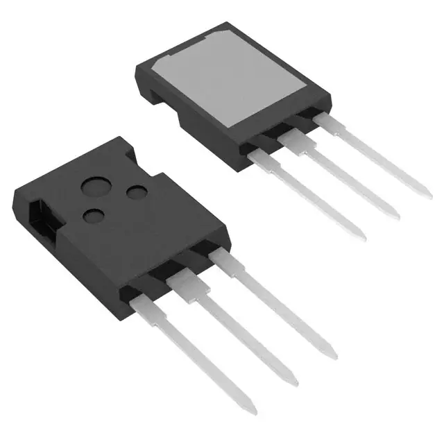
TO-264 AA
(IXGK)
(TAB)
G
C
E
PLUS247
(IXGX)
(TAB)
G = Gate
E = Emitter
C = Collector
Tab = Collector
Features
• Square RBSOA
• High current handling capability
• MOS Gate turn-on for drive simplicity
• Fast Recovery Epitaxial Diode (FRED)
with soft recovery and low IRM
Applications
• Switch-mode and resonant-mode
power supplies
• Uninterruptible power supplies (UPS)
• DC choppers
• AC motor speed control
• DC servo and robot drives
Advantages
• Space savings (two devices in one
package)
• Easy to mount with 1 screw
DS99114(11/03)
�IXGK 60N60B2D1
IXGX 60N60B2D1
Symbol
Test Conditions
Characteristic Values
(TJ = 25°C, unless otherwise specified)
Min. Typ. Max.
58
S
3900
340
pF
pF
Cres
100
pF
Qg
Qge
170
25
nC
nC
57
nC
gfs
Cies
Coes
IC = 50 A; VCE = 10 V,
Note 1
40
VCE = 25 V, VGE = 0 V, f = 1 MHz
IC = 50 A, VGE = 15 V, VCE = 0.5 VCES
Qgc
td(on)
Dim.
28
ns
30
ns
tri
Inductive load, TJ = 25°°C
td(off)
IC = 50 A, VGE = 15 V
160 270
ns
VCE = 400 V, RG = Roff = 3.3 Ω
100 170
ns
tfi
Eoff
1.0
2.5 mJ
td(on)
tri
Eon
td(off)
tfi
Eoff
28
36
1.5
310
240
2.8
ns
ns
mJ
ns
ns
mJ
0.15
0.25 K/W
K/W
Inductive load, TJ = 125°°C
IC = 50 A, VGE = 15 V
VCE = 400 V, RG = Roff = 2.0 Ω
RthJC
RthCK
Reverse Diode (FRED)
Symbol
Test Conditions
VF
IF = 60 A, VGE = 0 V,
Note 1
IRM
t rr
TO-264 AA Outline
Millimeter
Min.
Max.
A
A1
A2
b
b1
b2
c
D
E
e
J
K
L
L1
P
Q
Q1
R
R1
S
T
4.82
5.13
2.54
2.89
2.00
2.10
1.12
1.42
2.39
2.69
2.90
3.09
0.53
0.83
25.91
26.16
19.81
19.96
5.46 BSC
0.00
0.25
0.00
0.25
20.32
20.83
2.29
2.59
3.17
3.66
6.07
6.27
8.38
8.69
3.81
4.32
1.78
2.29
6.04
6.30
1.57
1.83
Min.
Inches
Max.
.190
.202
.100
.114
.079
.083
.044
.056
.094
.106
.114
.122
.021
.033
1.020
1.030
.780
.786
.215 BSC
.000
.010
.000
.010
.800
.820
.090
.102
.125
.144
.239
.247
.330
.342
.150
.170
.070
.090
.238
.248
.062
.072
PLUS247 Outline
Characteristic Values
(TJ = 25°C, unless otherwise specified)
min. typ. max.
TJ = 150°C
IF = 60 A, VGE = 0 V, -diF/dt = 100 A/µ TJ = 100°C
VR = 100 V
IF = 1 A; -di/dt = 200 A/ms; VR = 30 V
RthJC
35
2.1
1.4
V
V
8.3
A
ns
0.85 K/W
Note 1: Pulse test, t ≤ 300 µs, duty cycle ≤ 2 %
Terminals:
Dim.
A
A1
A2
b
b1
b2
C
D
E
e
L
L1
Q
R
1 - Gate
2 - Drain (Collector)
3 - Source (Emitter)
4 - Drain (Collector)
Millimeter
Min.
Max.
4.83
5.21
2.29
2.54
1.91
2.16
1.14
1.40
1.91
2.13
2.92
3.12
0.61
0.80
20.80 21.34
15.75 16.13
5.45 BSC
19.81 20.32
3.81
4.32
5.59
6.20
4.32
4.83
Inches
Min. Max.
.190 .205
.090 .100
.075 .085
.045 .055
.075 .084
.115 .123
.024 .031
.819 .840
.620 .635
.215 BSC
.780 .800
.150 .170
.220 0.244
.170 .190
IXYS reserves the right to change limits, test conditions, and dimensions.
IXYS MOSFETs and IGBTs are covered by one or more
of the following U.S. patents:
4,835,592 4,881,106 5,017,508 5,049,961 5,187,117 5,486,715 6,306,728B1 6,259,123B1 6,306,728B1
4,850,072 4,931,844 5,034,796 5,063,307 5,237,481 5,381,025 6,404,065B1 6,162,665
6,534,343
�IXGK 60N60B2D1
IXGX 60N60B2D1
Fig. 1. Output Characteristics
@ 25 Deg. C
Fig. 2. Extended Output Characteristics
@ 25 deg. C
350
100
VGE = 15V
13V
11V
90
80
300
11V
250
60
I C - Amperes
70
I C - Amperes
VGE = 15V
13V
9V
7V
50
40
30
9V
200
150
7V
100
20
10
50
5V
5V
0
0
0.5
1
1.5
2
2.5
3
0
1
2
3
Fig. 3. Output Characteristics
@ 125 Deg. C
5
6
7
8
Fig. 4. Dependence of V CE(sat) on
Tem perature
100
1.4
VGE = 15V
13V
11V
80
9V
V GE = 15V
1.3
70
V C E (sat)- Normalized
90
I C - Amperes
4
V C E - Volts
V C E - Volts
7V
60
50
40
30
I C = 100A
1.2
1.1
I C = 50A
1.0
0.9
0.8
20
0.7
5V
10
0
I C = 25A
0.6
0.5
1
1.5
2
2.5
3
-50
-25
0
V CE - Volts
25
50
75
100
125
150
TJ - Degrees Centigrade
Fig. 5. Collector-to-Em itter Voltage
vs. Gate-to-Em itter voltage
Fig. 6. Input Adm ittance
300
3.7
TJ = 25ºC
3.4
250
I C = 100A
50A
25A
2.8
2.5
I C - Amperes
VC E - Volts
3.1
2.2
200
150
100
1.9
TJ = 125ºC
-40ºC
50
TJ = 25ºC
1.6
0
1.3
5
6
7
8
9
10
11
12
V G E - Volts
© 2003 IXYS All rights reserved
13
14
15
16
17
4
5
6
7
V G E - Volts
8
9
10
�IXGK 60N60B2D1
IXGX 60N60B2D1
Fig. 8. Dependence of Turn-Off
Energy on RG
Fig. 7. Transconductance
100
10
90
9
TJ = -40ºC
25ºC
125ºC
g f s - Siemens
70
8
E off - milliJoules
80
60
50
40
30
I C = 100A
7
6
5
4
20
3
10
2
0
I C = 50A
I C = 25A
1
0
50
100
150
200
250
300
0
5
10
15
20
25
30
35
40
45
I C - Amperes
R G - Ohms
Fig. 9. Dependence of Turn-Off
Energy on Ic
Fig. 10. Dependence of Turn-Off
Energy on Tem perature
7
50
7
R G = 3.3Ω
VGE = 15V
VCE = 400V
6
5
4
R G = 3.3Ω
VGE = 15V
VCE = 400V
6
E off - milliJoules
E off - MilliJoules
TJ = 125ºC
VGE = 15V
VCE = 400V
TJ = 125ºC
3
2
TJ = 25ºC
1
5
I C = 100A
4
3
I C = 50A
2
1
I C = 25A
0
0
20
30
40
50
60
70
80
90
100
25
35
I C - Amperes
55
65
75
85
95
105 115 125
TJ - Degrees Centigrade
Fig. 11. Dependence of Turn-Off
Sw itching Tim e on RG
Fig. 12. Dependence of Turn-Off
Sw itching Tim e on Ic
1200
400
1000
Switching Time - nanosecond
td(off)
tfi - - - - - -
1100
Switching Time - nanosecond
45
TJ = 125ºC
VGE = 15V
VCE = 400V
900
800
700
600
I C = 25A
500
I C = 50A
400
I C = 100A
300
200
td(off)
tfi - - - - - -
350
R G = 3.3Ω
VGE = 15V
VCE = 400V
300
TJ = 125ºC
250
200
150
TJ = 25ºC
100
50
0
5
10
15
20
25
30
35
40
45
50
R G - Ohms
IXYS reserves the right to change limits, test conditions, and dimensions.
20
30
40
50
60
70
I C - Amperes
80
90
100
�IXGK 60N60B2D1
IXGX 60N60B2D1
Fig. 13. Dependence of Turn-Off
Sw itching Tim e on Tem perature
Fig. 14. Gate Charge
15
td(off)
tfi - - - - - -
300
I C = 25A
50A
100A
R G = 3.3Ω
VGE = 15V
VCE = 400V
250
200
150
I C = 100A
50A
25A
100
VCE = 300V
I C = 50A
I G = 10mA
12
VG E - Volts
Switching Time - nanosecond
350
9
6
3
50
0
25
35
45
55
65
75
85
95
105 115 125
0
20
TJ - Degrees Centigrade
40
60
80
100
120
140
160
180
Q G - nanoCoulombs
Fig. 15. Capacitance
10000
Capacitance - p F
f = 1 MHz
C ies
1000
C oes
100
C res
10
0
5
10
15
20
25
30
35
40
V C E - Volts
Fig. 16. Maxim um Transient Therm al Resistance
0.275
0.25
R (th) J C - (ºC/W)
0.225
0.2
0.175
0.15
0.125
0.1
0.075
0.05
1
10
100
Pulse Width - milliseconds
© 2003 IXYS All rights reserved
1000
�IXGK 60N60B2D1
IXGX 60N60B2D1
160
A
140
IF
4000
nC
120
80
TVJ= 100°C
VR = 300V
3000
TVJ= 25°C
60
IF=120A
IF= 60A
IF= 30A
Qr
100
TVJ=100°C
80
TVJ= 100°C
VR = 300V
A
IRM
2000
40
1000
20
IF=120A
IF= 60A
IF= 30A
TVJ=150°C
60
40
20
0
0
1
2
0
100
V
0
A/µs 1000
-diF/dt
VF
Fig. 17. Forward current IF versus VF
Fig. 18. Reverse recovery charge Qr
versus -diF/dt
140
2.0
TVJ= 100°C
VR = 300V
ns
130
trr
1.5
Kf
0
400
600 A/µs
800 1000
-diF/dt
Fig. 19. Peak reverse current IRM
versus -diF/dt
20
1.6
V
VFR
15
µs
tfr
IF=120A
IF= 60A
IF= 30A
110
1.2
VFR
tfr
120
1.0
200
10
0.8
5
0.4
IRM
100
0.5
Qr
90
0.0
80
0
40
80
120 °C 160
0
0
200
400
600
TVJ
800 1000
A/µs
0
200
400
-diF/dt
Fig. 20. Dynamic parameters Qr, IRM
versus TVJ
Fig. 21. Recovery time trr versus -diF/dt
1
0.0
600 A/µs
800 1000
diF/dt
Fig. 22. Peak forward voltage VFR and
tfr
versus diF/dt
Constants for ZthJC calculation:
K/W
i
0.1
1
2
3
4
ZthJC
0.01
0.001
0.0001
0.00001
TVJ= 100°C
IF = 60A
DSEP 2x61-06A
0.0001
0.001
0.01
s
0.1
t
Fig. 23. Transient thermal resistance junction to case
IXYS reserves the right to change limits, test conditions, and dimensions.
1
Rthi (K/W)
ti (s)
0.3073
0.3533
0.0887
0.1008
0.0055
0.0092
0.0007
0.0399
�


 工商网监
湘ICP备2023018690号
工商网监
湘ICP备2023018690号
