ON Semiconductor
Is Now
To learn more about onsemi™, please visit our website at
www.onsemi.com
onsemi and and other names, marks, and brands are registered and/or common law trademarks of Semiconductor Components Industries, LLC dba “onsemi” or its affiliates and/or
subsidiaries in the United States and/or other countries. onsemi owns the rights to a number of patents, trademarks, copyrights, trade secrets, and other intellectual property. A listing of onsemi
product/patent coverage may be accessed at www.onsemi.com/site/pdf/Patent-Marking.pdf. onsemi reserves the right to make changes at any time to any products or information herein, without
notice. The information herein is provided “as-is” and onsemi makes no warranty, representation or guarantee regarding the accuracy of the information, product features, availability, functionality,
or suitability of its products for any particular purpose, nor does onsemi assume any liability arising out of the application or use of any product or circuit, and specifically disclaims any and all
liability, including without limitation special, consequential or incidental damages. Buyer is responsible for its products and applications using onsemi products, including compliance with all laws,
regulations and safety requirements or standards, regardless of any support or applications information provided by onsemi. “Typical” parameters which may be provided in onsemi data sheets and/
or specifications can and do vary in different applications and actual performance may vary over time. All operating parameters, including “Typicals” must be validated for each customer application
by customer’s technical experts. onsemi does not convey any license under any of its intellectual property rights nor the rights of others. onsemi products are not designed, intended, or authorized
for use as a critical component in life support systems or any FDA Class 3 medical devices or medical devices with a same or similar classification in a foreign jurisdiction or any devices intended for
implantation in the human body. Should Buyer purchase or use onsemi products for any such unintended or unauthorized application, Buyer shall indemnify and hold onsemi and its officers, employees,
subsidiaries, affiliates, and distributors harmless against all claims, costs, damages, and expenses, and reasonable attorney fees arising out of, directly or indirectly, any claim of personal injury or death
associated with such unintended or unauthorized use, even if such claim alleges that onsemi was negligent regarding the design or manufacture of the part. onsemi is an Equal Opportunity/Affirmative
Action Employer. This literature is subject to all applicable copyright laws and is not for resale in any manner. Other names and brands may be claimed as the property of others.
�CAT24C164
16 kb CMOS Serial
EEPROM, Cascadable
Description
The CAT24C164 is a 16 kb CMOS cascadable Serial EEPROM
device organized internally as 128 pages of 16 bytes each, for a total of
2048 x 8 bits. The device supports both the Standard (100 kHz) as well
as Fast (400 kHz) I2C protocol.
Data is written by providing a starting address, then loading 1 to 16
contiguous bytes into a Page Write Buffer, and then writing all data to
non−volatile memory in one internal write cycle. Data is read by
providing a starting address and then shifting out data serially while
automatically incrementing the internal address count.
External address pins make it possible to address up to eight
CAT24C164 devices on the same bus.
http://onsemi.com
SOIC−8
W SUFFIX
CASE 751BD
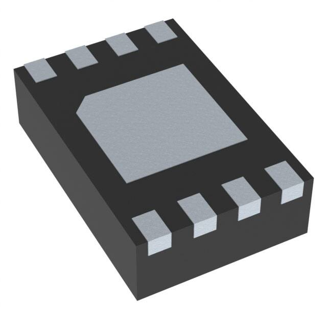
TDFN−8
VP2 SUFFIX
CASE 511AK
PDIP−8
L SUFFIX
CASE 646AA
TSSOP−8
Y SUFFIX
CASE 948AL
Features
•
•
•
•
•
•
•
•
•
•
•
Supports Standard and Fast I2C Protocol
1.8 V to 5.5 V Supply Voltage Range
16−Byte Page Write Buffer
Hardware Write Protection for Entire Memory
Schmitt Triggers and Noise Suppression Filters on I2C Bus Inputs
(SCL and SDA)
Low Power CMOS Technology
1,000,000 Program/Erase Cycles
100 Year Data Retention
Industrial Temperature Range
PDIP, SOIC, TSSOP and TDFN 8−lead Packages
This Device is Pb−Free, Halogen Free/BFR Free, and RoHS
Compliant
VCC
PIN CONFIGURATION
A0
1
VCC
A1
WP
A2
SCL
VSS
SDA
PDIP (L), SOIC (W),
TSSOP (Y), TDFN (VP2)
(Top View)
For the location of Pin 1, please consult the
corresponding package drawing.
PIN FUNCTION
SCL
Pin Name
CAT24C164
A2, A1, A0
A0, A1, A2
SDA
WP
VSS
Figure 1. Functional Symbol
Function
Device Address Inputs
SDA
Serial Data Input/Output
SCL
Serial Clock Input
WP
Write Protect Input
VCC
Power Supply
VSS
Ground
ORDERING INFORMATION
See detailed ordering and shipping information in the package
dimensions section on page 14 of this data sheet.
© Semiconductor Components Industries, LLC, 2009
October, 2009 − Rev. 2
1
Publication Order Number:
CAT24C164/D
�CAT24C164
Table 1. ABSOLUTE MAXIMUM RATINGS
Parameters
Ratings
Units
Storage Temperature
–65 to +150
°C
Voltage on Any Pin with Respect to Ground (Note 1)
–0.5 to +6.5
V
Stresses exceeding Maximum Ratings may damage the device. Maximum Ratings are stress ratings only. Functional operation above the
Recommended Operating Conditions is not implied. Extended exposure to stresses above the Recommended Operating Conditions may affect
device reliability.
1. The DC input voltage on any pin should not be lower than −0.5 V or higher than VCC + 0.5 V. During transitions, the voltage on any pin may
undershoot to no less than −1.5 V or overshoot to no more than VCC + 1.5 V, for periods of less than 20 ns.
Table 2. RELIABILITY CHARACTERISTICS (Note 2)
Symbol
NEND (Note 3)
TDR
Parameter
Endurance
Data Retention
Min
Units
1,000,000
Program/Erase Cycles
100
Years
2. These parameters are tested initially and after a design or process change that affects the parameter according to appropriate AEC−Q100
and JEDEC test methods.
3. Page Mode, VCC = 5 V, 25°C.
Table 3. D.C. OPERATING CHARACTERISTICS (VCC = 1.8 V to 5.5 V, TA = −40°C to +85°C, unless otherwise specified.)
Parameter
Symbol
Test Conditions
Min
Max
Units
ICCR
Read Current
Read, fSCL = 400 kHz
1
mA
ICCW
Write Current
Write, fSCL = 400 kHz
1
mA
ISB
Standby Current
All I/O Pins at GND or VCC
1
mA
IL
I/O Pin Leakage
Pin at GND or VCC
1
mA
−0.5
VCC x 0.3
V
VCC x 0.7
VIL
Input Low Voltage
VIH
Input High Voltage
VCC + 0.5
V
VOL1
Output Low Voltage
VCC ≥ 2.5 V, IOL = 3.0 mA
0.4
V
VOL2
Output Low Voltage
VCC < 2.5 V, IOL = 1.0 mA
0.2
V
Table 4. PIN IMPEDANCE CHARACTERISTICS (VCC = 1.8 V to 5.5 V, TA = −40°C to +85°C, unless otherwise specified.)
Symbol
Parameter
Conditions
Max
Units
CIN (Note 4)
SDA I/O Pin Capacitance
VIN = 0 V
8
pF
CIN (Note 4)
Input Capacitance (other pins)
VIN = 0 V
6
pF
IWP (Note 5)
WP Input Current
VIN < VIH, VCC = 5.5 V
200
mA
VIN < VIH, VCC = 3.3 V
150
VIN < VIH, VCC = 1.8 V
100
VIN > VIH
1
4. These parameters are tested initially and after a design or process change that affects the parameter according to appropriate AEC−Q100
and JEDEC test methods.
5. When not driven, the WP pin is pulled down to GND internally. For improved noise immunity, the internal pull−down is relatively strong;
therefore the external driver must be able to supply the pull−down current when attempting to drive the input HIGH. To conserve power, as
the input level exceeds the trip point of the CMOS input buffer (~ 0.5 x VCC), the strong pull−down reverts to a weak current source.
http://onsemi.com
2
�CAT24C164
Table 5. A.C. CHARACTERISTICS (VCC = 1.8 V to 5.5 V, TA = −40°C to +85°C.) (Note 6)
Standard
FSCL
tHD:STA
Clock Frequency
Max
Min
100
START Condition Hold Time
Max
Units
400
kHz
4
0.6
ms
tLOW
Low Period of SCL Clock
4.7
1.3
ms
tHIGH
High Period of SCL Clock
4
0.6
ms
4.7
0.6
ms
tSU:STA
START Condition Setup Time
tHD:DAT
Data In Hold Time
0
0
ms
tSU:DAT
Data In Setup Time
250
100
ns
tR
SDA and SCL Rise Time
tF (Note 7)
SDA and SCL Fall Time
tSU:STO
1000
300
STOP Condition Setup Time
tBUF
Bus Free Time Between STOP and START
tAA
SCL Low to Data Out Valid
tDH
Data Out Hold Time
Ti (Note 7)
ns
300
ns
0.6
ms
4.7
1.3
ms
3.5
100
Noise Pulse Filtered at SCL and SDA Inputs
0.9
100
100
WP Setup Time
0
0
WP Hold Time
2.5
2.5
ms
ns
100
tSU:WP
tPU (Notes 7, 8)
300
4
tHD:WP
tWR
6.
7.
8.
Min
Parameter
Symbol
Fast
ns
ms
ms
Write Cycle Time
5
5
ms
Power-up to Ready Mode
1
1
ms
Test conditions according to “A.C. Test Conditions” table.
Tested initially and after a design or process change that affects this parameter.
tPU is the delay between the time VCC is stable and the device is ready to accept commands.
Table 6. A.C. TEST CONDITIONS
Input Levels
0.2 x VCC to 0.8 x VCC
Input Rise and Fall Times
≤ 50 ns
Input Reference Levels
0.3 x VCC, 0.7 x VCC
Output Reference Levels
0.5 x VCC
Output Load
Current Source: IOL = 3 mA (VCC ≥ 2.5 V); IOL = 1 mA (VCC < 2.5 V); CL = 100 pF
http://onsemi.com
3
�CAT24C164
Power-On Reset (POR)
CAT24C164 incorporates Power−On Reset (POR)
circuitry which protects the internal logic against powering
up in the wrong state.
A CAT24C164 device will power up into Standby mode
after VCC exceeds the POR trigger level and will power
down into Reset mode when VCC drops below the POR
trigger level. This bi−directional POR feature protects the
device against ‘brown−out’ failure following a temporary
loss of power.
device pulls down the SDA line to ‘transmit’ a ‘0’ and
releases it to ‘transmit’ a ‘1’.
Data transfer may be initiated only when the bus is not
busy (see A.C. Characteristics).
During data transfer, the SDA line must remain stable
while the SCL line is HIGH. An SDA transition while SCL
is HIGH will be interpreted as a START or STOP condition
(Figure 2). The START condition precedes all commands. It
consists of a HIGH to LOW transition on SDA while SCL
is HIGH. The START acts as a ‘wake−up’ call to all
receivers. Absent a START, a Slave will not respond to
commands. The STOP condition completes all commands.
It consists of a LOW to HIGH transition on SDA while SCL
is HIGH.
Pin Description
SCL: The Serial Clock input pin accepts the Serial Clock
generated by the Master.
SDA: The Serial Data I/O pin receives input data and
transmits data stored in EEPROM. In transmit mode, this pin
is open drain. Data is acquired on the positive edge, and is
delivered on the negative edge of SCL.
A0, A1 and A2: The Address inputs set the device address
when cascading multiple devices. When not driven, these
pins are pulled LOW internally.
The CAT24C164 can be made compatible with the
CAT24C16 by tying A2, A1 and A0 to VSS or by leaving A2,
A1 and A0 float.
WP: The Write Protect input pin inhibits all write
operations, when pulled HIGH. When not driven, this pin is
pulled LOW internally.
Device Addressing
The bus Master begins a transmission by sending a
START condition. The Master then sends the address of the
particular Slave device it is requesting. The most significant
bit of the 8−bit slave address is fixed as 1. (see Figure 3). The
next three significant bits (A2, A1, A0) are the device address
bits and define which device or which part of the device the
Master is accessing (The A1 bit must be the compliment of
the A1 input pin signal). Up to eight CAT24C164 devices
may be individually addressed by the system. The next three
bits are used as the three most significant bits of the data
word address. The last bit of the slave address specifies
whether a Read or Write operation is to be performed. When
this bit is set to 1, a Read operation is selected, and when set
to 0, a Write operation is selected.
Functional Description
The CAT24C164 supports the Inter−Integrated Circuit
(I2C) Bus data transmission protocol, which defines a device
that sends data to the bus as a transmitter and a device
receiving data as a receiver. Data flow is controlled by a
Master device, which generates the serial clock and all
START and STOP conditions. The CAT24C164 acts as a
Slave device. Master and Slave alternate as either
transmitter or receiver.
Acknowledge
After processing the Slave address, the Slave responds
with an acknowledge (ACK) by pulling down the SDA line
during the 9th clock cycle (Figure 4). The Slave will also
acknowledge the address byte and every data byte presented
in Write mode. In Read mode the Slave shifts out a data byte,
and then releases the SDA line during the 9th clock cycle. As
long as the Master acknowledges the data, the Slave will
continue transmitting. The Master terminates the session by
not acknowledging the last data byte (NoACK) and by
issuing a STOP condition. Bus timing is illustrated in
Figure 5.
I2C Bus Protocol
The I2C bus consists of two ‘wires’, SCL and SDA. The
two wires are connected to the VCC supply via pull−up
resistors. Master and Slave devices connect to the 2−wire
bus via their respective SCL and SDA pins. The transmitting
http://onsemi.com
4
�CAT24C164
SCL
SDA
START
CONDITION
STOP
CONDITION
Figure 2. START/STOP Conditions
1
A2
A1
A0
a10
a9
a8
R/W
CAT24C164
Figure 3. Slave Address Bits
BUS RELEASE DELAY (TRANSMITTER)
SCL FROM
MASTER
1
BUS RELEASE DELAY (RECEIVER)
8
9
DATA OUTPUT
FROM TRANSMITTER
DATA OUTPUT
FROM RECEIVER
START
ACK SETUP (≥ tSU:DAT)
ACK DELAY (≤ tAA)
Figure 4. Acknowledge Timing
tHIGH
tF
tLOW
tR
tLOW
SCL
tSU:STA
tHD:DAT
tHD:STA
tSU:DAT
tSU:STO
SDA IN
tAA
tDH
SDA OUT
Figure 5. Bus Timing
http://onsemi.com
5
tBUF
�CAT24C164
WRITE OPERATIONS
Byte Write
sixteen bytes are received and the STOP condition has been
sent by the Master, the internal Write cycle begins. At this
point all received data is written to the CAT24C164 in a
single write cycle.
In Byte Write mode, the Master sends the START
condition and the Slave address with the R/W bit set to zero
to the Slave. After the Slave generates an acknowledge, the
Master sends the byte address that is to be written into the
address pointer of the CAT24C164. After receiving another
acknowledge from the Slave, the Master transmits the data
byte to be written into the addressed memory location. The
CAT24C164 device will acknowledge the data byte and the
Master generates the STOP condition, at which time the
device begins its internal Write cycle to nonvolatile memory
(Figure 6). While this internal cycle is in progress (tWR), the
SDA output will be tri−stated and the CAT24C164 will not
respond to any request from the Master device (Figure 7).
Acknowledge Polling
The acknowledge (ACK) polling routine can be used to
take advantage of the typical write cycle time. Once the stop
condition is issued to indicate the end of the host’s write
operation, the CAT24C164 initiates the internal write cycle.
The ACK polling can be initiated immediately. This
involves issuing the start condition followed by the slave
address for a write operation. If the CAT24C164 is still busy
with the write operation, NoACK will be returned. If the
CAT24C164 has completed the internal write operation, an
ACK will be returned and the host can then proceed with the
next read or write operation.
Page Write
The CAT24C164 writes up to 16 bytes of data in a single
write cycle, using the Page Write operation (Figure 8). The
Page Write operation is initiated in the same manner as the
Byte Write operation, however instead of terminating after
the data byte is transmitted, the Master is allowed to send up
to fifteen additional bytes. After each byte has been
transmitted the CAT24C164 will respond with an
acknowledge and internally increments the four low order
address bits. The high order bits that define the page address
remain unchanged. If the Master transmits more than sixteen
bytes prior to sending the STOP condition, the address
counter ‘wraps around’ to the beginning of page and
previously transmitted data will be overwritten. Once all
Hardware Write Protection
With the WP pin held HIGH, the entire memory is
protected against Write operations. If the WP pin is left
floating or is grounded, it has no impact on the operation of
the CAT24C164. The state of the WP pin is strobed on the
last falling edge of SCL immediately preceding the first data
byte (Figure 9). If the WP pin is HIGH during the strobe
interval, the CAT24C164 will not acknowledge the data byte
and the Write request will be rejected.
Delivery State
The CAT24C164 is shipped erased, i.e., all bytes are FFh.
http://onsemi.com
6
�CAT24C164
BUS ACTIVITY: S
T
A
MASTER R
T
SLAVE
ADDRESS
ADDRESS
BYTE
DATA
BYTE
a7 − a0
d7 − d0
S
T
O
P
P
S
SLAVE
A
C
K
A
C
K
A
C
K
Figure 6. Byte Write Sequence
SCL
SDA
8th Bit
Byte n
ACK
tWR
STOP
CONDITION
START
CONDITION
ADDRESS
Figure 7. Write Cycle Timing
BUS
ACTIVITY:
MASTER
S
T
A
R
T
DATA
BYTE
n
ADDRESS
BYTE
SLAVE
ADDRESS
DATA
BYTE
n+1
DATA
BYTE
n+P
S
T
O
P
P
S
A
C
K
SLAVE
n=1
P ≤ 15
A
C
K
A
C
K
A
C
K
A
C
K
Figure 8. Page Write Sequence
ADDRESS
BYTE
DATA
BYTE
1
8
a7
a0
9
1
8
d7
d0
SCL
SDA
tSU:WP
WP
tHD:WP
Figure 9. WP Timing
http://onsemi.com
7
�CAT24C164
READ OPERATIONS
Immediate Read
address of the location it wishes to read. After the
CAT24C164 acknowledges the byte address, the Master
device resends the START condition and the slave address,
this time with the R/W bit set to one. The CAT24C164 then
responds with its acknowledge and sends the requested data
byte. The Master device does not acknowledge the data
(NoACK) but will generate a STOP condition (Figure 11).
Upon receiving a Slave address with the R/W bit set to ‘1’,
the CAT24C164 will interpret this as a request for data
residing at the current byte address in memory. The
CAT24C164 will acknowledge the Slave address, will
immediately shift out the data residing at the current address,
and will then wait for the Master to respond. If the Master
does not acknowledge the data (NoACK) and then follows
up with a STOP condition (Figure 10), the CAT24C164
returns to Standby mode.
Sequential Read
If during a Read session, the Master acknowledges the 1st
data byte, then the CAT24C164 will continue transmitting
data residing at subsequent locations until the Master
responds with a NoACK, followed by a STOP (Figure 12).
In contrast to Page Write, during Sequential Read the
address count will automatically increment to and then
wrap−around at end of memory (rather than end of page).
Selective Read
Selective Read operations allow the Master device to
select at random any memory location for a read operation.
The Master device first performs a ‘dummy’ write operation
by sending the START condition, slave address and byte
BUS ACTIVITY:
MASTER
N
O
S
T
A
R
T
S
A T
CO
K P
SLAVE
ADDRESS
S
P
A
C
K
SLAVE
SCL
DATA
BYTE
8
SDA
9
8th Bit
DATA OUT
NO ACK
STOP
Figure 10. Immediate Read Sequence and Timing
BUS ACTIVITY:
MASTER
S
T
A
R
T
S
T
A
R
T
ADDRESS
BYTE
SLAVE
ADDRESS
N
O
A
C
K
SLAVE
ADDRESS
S
S
A
C
K
SLAVE
S
T
O
P
P
A
C
K
A
C
K
DATA
BYTE
Figure 11. Selective Read Sequence
N
O
A
C
K
BUS ACTIVITY:
MASTER
A
C
K
SLAVE
ADDRESS
A
C
K
A
C
K
S
T
O
P
P
SLAVE
A
C
K
DATA
BYTE
n
DATA
BYTE
n+1
DATA
BYTE
n+2
Figure 12. Sequential Read Sequence
http://onsemi.com
8
DATA
BYTE
n+x
�CAT24C164
PACKAGE DIMENSIONS
PDIP−8, 300 mils
CASE 646AA−01
ISSUE A
SYMBOL
MIN
NOM
A
E1
5.33
A1
0.38
A2
2.92
3.30
4.95
b
0.36
0.46
0.56
b2
1.14
1.52
1.78
c
0.20
0.25
0.36
D
9.02
9.27
10.16
E
7.62
7.87
8.25
E1
6.10
6.35
7.11
e
PIN # 1
IDENTIFICATION
MAX
2.54 BSC
eB
7.87
L
2.92
10.92
3.30
3.80
D
TOP VIEW
E
A2
A
A1
c
b2
L
e
eB
b
SIDE VIEW
END VIEW
Notes:
(1) All dimensions are in millimeters.
(2) Complies with JEDEC MS-001.
http://onsemi.com
9
�CAT24C164
PACKAGE DIMENSIONS
SOIC 8, 150 mils
CASE 751BD−01
ISSUE O
E1
E
SYMBOL
MIN
A
1.35
1.75
A1
0.10
0.25
b
0.33
0.51
c
0.19
0.25
D
4.80
5.00
E
5.80
6.20
E1
3.80
MAX
4.00
1.27 BSC
e
PIN # 1
IDENTIFICATION
NOM
h
0.25
0.50
L
0.40
1.27
θ
0º
8º
TOP VIEW
D
h
A1
θ
A
c
e
b
L
SIDE VIEW
END VIEW
Notes:
(1) All dimensions are in millimeters. Angles in degrees.
(2) Complies with JEDEC MS-012.
http://onsemi.com
10
�CAT24C164
PACKAGE DIMENSIONS
TSSOP8, 4.4x3
CASE 948AL−01
ISSUE O
b
SYMBOL
MIN
NOM
A
E1
E
MAX
1.20
A1
0.05
A2
0.80
b
0.19
0.15
0.90
1.05
0.30
c
0.09
D
2.90
3.00
3.10
E
6.30
6.40
6.50
E1
4.30
4.40
4.50
e
0.20
0.65 BSC
L
1.00 REF
L1
0.50
θ
0º
0.60
0.75
8º
e
TOP VIEW
D
A2
c
q1
A
A1
L1
SIDE VIEW
L
END VIEW
Notes:
(1) All dimensions are in millimeters. Angles in degrees.
(2) Complies with JEDEC MO-153.
http://onsemi.com
11
�CAT24C164
PACKAGE DIMENSIONS
TDFN8, 2x3
CASE 511AK−01
ISSUE A
D
A
e
b
E2
E
PIN#1
IDENTIFICATION
A1
PIN#1 INDEX AREA
D2
TOP VIEW
SIDE VIEW
SYMBOL
MIN
NOM
MAX
A
0.70
0.75
0.80
A1
0.00
0.02
0.05
A2
0.45
0.55
0.65
A3
A2
A3
0.20
0.25
0.30
D
1.90
2.00
2.10
D2
1.30
1.40
1.50
E
2.90
3.00
3.10
E2
1.20
1.30
1.40
L
BOTTOM VIEW
0.20 REF
b
e
FRONT VIEW
0.50 TYP
0.20
0.30
L
0.40
Notes:
(1) All dimensions are in millimeters.
(2) Complies with JEDEC MO-229.
http://onsemi.com
12
�CAT24C164
Package Marking
I
YY
WW
G
F
8−Lead PDIP
8−Lead SOIC
24C164LI
FYYWW G
24C164WI
FYYWWG
= Temperature Range
= Production Year
= Production Week
= Product Revision
= Lead Finish
= 4 = NiPdAu
I
YY
WW
G
F
8−Lead TSSOP
8−Pad TDFN
XXN
YMGF
NNN
24164I
Y
M
G
I
F
= Temperature Range
= Production Year
= Production Week
= Product Revision
= Lead Finish
= 4 = NiPdAu
YM
= Production Year
= Production Month
= Die Revision
= Temperature Range
= Lead Finish
= 4 = NiPdAu
XX
N
Y
M
9. The circle on the package marking indicates the location of Pin 1.
10. For TDFN package, the Product Revision marking is included in the Device Code (XX).
http://onsemi.com
13
= Device Code
= FR = NiPdAu
= Traceable Code
= Production Year
= Production Month
�CAT24C164
Example of Ordering Information
Prefix
Device #
Suffix
CAT
24C164
Y
I
−G
Temperature Range
Lead Finish
I = Industrial (−40°C to +85°C)
E = Extended (−40°C to +125°C)
G: NiPdAu
Company ID
Product Number
24C164
T3
Tape & Reel (Note 16)
T: Tape & Reel
3: 3,000 / Reel
Package
L: PDIP
W: SOIC, JEDEC
Y: TSSOP
VP2: TDFN
ORDERING INFORMATION
Orderable Part Numbers
CAT24C164LI−G
CAT24C164LE−G
CAT24C164WI−GT3
CAT24C164WE−GT3
CAT24C164YI−GT3
CAT24C164YE−GT3
CAT24C164VP2IGT3 (Note 15)
CAT24C164VP2EGT3 (Note 15)
11. All packages are RoHS-compliant (Lead-free, Halogen-free).
12. The standard lead finish is NiPdAu.
13. The device used in the above example is a CAT24C164YI−GT3 (TSSOP, Industrial Temperature, NiPdAu, Tape & Reel, 3,000/Reel).
14. For additional package and temperature options, please contact your nearest ON Semiconductor Sales office.
15. Part number is not exactly the same as the “Example of Ordering Information” shown above. For the part numbers indicated there are NO
hyphens in the orderable part numbers.
16. For information on tape and reel specifications, including part orientation and tape sizes, please refer to our Tape and Reel Packaging
Specifications Brochure, BRD8011/D.
ON Semiconductor is licensed by Philips Corporation to carry the I2C Bus Protocol.
ON Semiconductor and
are registered trademarks of Semiconductor Components Industries, LLC (SCILLC). SCILLC reserves the right to make changes without further notice
to any products herein. SCILLC makes no warranty, representation or guarantee regarding the suitability of its products for any particular purpose, nor does SCILLC assume any liability
arising out of the application or use of any product or circuit, and specifically disclaims any and all liability, including without limitation special, consequential or incidental damages.
“Typical” parameters which may be provided in SCILLC data sheets and/or specifications can and do vary in different applications and actual performance may vary over time. All
operating parameters, including “Typicals” must be validated for each customer application by customer’s technical experts. SCILLC does not convey any license under its patent rights
nor the rights of others. SCILLC products are not designed, intended, or authorized for use as components in systems intended for surgical implant into the body, or other applications
intended to support or sustain life, or for any other application in which the failure of the SCILLC product could create a situation where personal injury or death may occur. Should
Buyer purchase or use SCILLC products for any such unintended or unauthorized application, Buyer shall indemnify and hold SCILLC and its officers, employees, subsidiaries, affiliates,
and distributors harmless against all claims, costs, damages, and expenses, and reasonable attorney fees arising out of, directly or indirectly, any claim of personal injury or death
associated with such unintended or unauthorized use, even if such claim alleges that SCILLC was negligent regarding the design or manufacture of the part. SCILLC is an Equal
Opportunity/Affirmative Action Employer. This literature is subject to all applicable copyright laws and is not for resale in any manner.
PUBLICATION ORDERING INFORMATION
LITERATURE FULFILLMENT:
Literature Distribution Center for ON Semiconductor
P.O. Box 5163, Denver, Colorado 80217 USA
Phone: 303−675−2175 or 800−344−3860 Toll Free USA/Canada
Fax: 303−675−2176 or 800−344−3867 Toll Free USA/Canada
Email: orderlit@onsemi.com
N. American Technical Support: 800−282−9855 Toll Free
USA/Canada
Europe, Middle East and Africa Technical Support:
Phone: 421 33 790 2910
Japan Customer Focus Center
Phone: 81−3−5773−3850
http://onsemi.com
14
ON Semiconductor Website: www.onsemi.com
Order Literature: http://www.onsemi.com/orderlit
For additional information, please contact your local
Sales Representative
CAT24C164/D
�


 工商网监
湘ICP备2023018690号
工商网监
湘ICP备2023018690号
