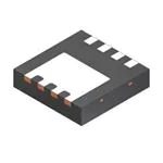
N-Channel PowerTrench® MOSFET General Description
80 V, 130 A, 2.4 mΩ
Features
Max rDS(on) = 2.4 mΩ at VGS = 10 V, ID = 25 A
This
N-Channel
MOSFET
is
produced using ON
Semiconductor‘s advanced Power Trench® process that has
been especially tailored to minimize the on-state resistance and
yet maintain superior switching performance.
Max rDS(on) = 3.2 mΩ at VGS = 8 V, ID = 22 A
Applications
Advanced Package and Silicon combination for low rDS(on)
and high efficiency
Primary MOSFET
MSL1 robust package design
Synchronous Rectifier
100% UIL tested
Load Switch
RoHS Compliant
Motor Control Switch
Bottom
Top
S
Pin 1
D
D
D
S
S
Pin 1
S
D
G
S
D
S
D
G
D
D
Power 56
MOSFET Maximum Ratings TA = 25 °C unless otherwise noted
Symbol
VDS
Drain to Source Voltage
Parameter
VGS
Gate to Source Voltage
Drain Current -Continuous
TC = 25 °C
-Continuous
TA = 25 °C
ID
-Pulsed
Single Pulse Avalanche Energy
EAS
PD
TJ, TSTG
TC = 25 °C
Power Dissipation
TA = 25 °C
Units
V
±20
V
130
(Note 1a)
25
(Note 4)
300
(Note 3)
Power Dissipation
Ratings
80
A
864
mJ
156
(Note 1a)
Operating and Storage Junction Temperature Range
W
2.7
-55 to +150
°C
Thermal Characteristics
RθJC
Thermal Resistance, Junction to Case
RθJA
Thermal Resistance, Junction to Ambient
0.8
(Note 1a)
45
°C/W
Package Marking and Ordering Information
Device Marking
FDMS86350
Device
FDMS86350
©2013 Semiconductor Components Industries, LLC
August-2017, Rev. 2
Package
Power 56
Reel Size
13 ’’
Tape Width
12 mm
Quantity
3000 units
Publication Order number:
FDMS86350/D
FDMS86350 N-Channel PowerTrench® MOSFET
FDMS86350
�Symbol
Parameter
Test Conditions
Min
Typ
Max
Units
Off Characteristics
BVDSS
Drain to Source Breakdown Voltage
ID = 250 μA, VGS = 0 V
ΔBVDSS
ΔTJ
Breakdown Voltage Temperature
Coefficient
ID = 250 μA, referenced to 25 °C
IDSS
Zero Gate Voltage Drain Current
VDS = 64 V, VGS = 0 V
1
μA
IGSS
Gate to Source Leakage Current
VGS = ±20 V, VDS = 0 V
±100
nA
4.5
V
80
V
45
mV/°C
On Characteristics
VGS(th)
Gate to Source Threshold Voltage
VGS = VDS, ID = 250 μA
ΔVGS(th)
ΔTJ
Gate to Source Threshold Voltage
Temperature Coefficient
ID = 250 μA, referenced to 25 °C
rDS(on)
Static Drain to Source On Resistance
gFS
Forward Transconductance
2.5
3.8
-12
mV/°C
VGS = 10 V, ID = 25 A
2.0
2.4
VGS = 8 V, ID = 22 A
2.5
3.2
VGS = 10 V, ID = 25 A, TJ = 125 °C
3.1
3.8
VDS = 5 V, ID = 25 A
70
mΩ
S
Dynamic Characteristics
Ciss
Input Capacitance
Coss
Output Capacitance
Crss
Reverse Transfer Capacitance
Rg
Gate Resistance
VDS = 40 V, VGS = 0 V,
f = 1 MHz
0.1
8030
10680
pF
1370
1825
pF
31
50
pF
1.1
3
Ω
50
80
ns
Switching Characteristics
td(on)
Turn-On Delay Time
tr
Rise Time
td(off)
Turn-Off Delay Time
tf
Fall Time
Qg
VDD = 40 V, ID = 25 A,
VGS = 10 V, RGEN = 6 Ω
34
55
ns
40
65
ns
11
20
ns
Total Gate Charge
VGS = 0 V to 10 V
110
155
nC
Qg
Total Gate Charge
VGS = 0 V to 8 V
90
127
Qgs
Gate to Source Charge
Qgd
Gate to Drain “Miller” Charge
VDD = 40 V,
ID = 25 A
nC
46
nC
23
nC
Drain-Source Diode Characteristics
IS
Diode Continuous Forward Current
TC = 25 °C
130
A
IS, pulse
Diode Pulse Current
TC = 25 °C
300
A
VSD
Source to Drain Diode Forward Voltage
trr
Reverse Recovery Time
Qrr
Reverse Recovery Charge
VGS = 0 V, IS = 2.1 A
(Note 2)
0.71
1.2
VGS = 0 V, IS = 25 A
(Note 2)
0.79
1.3
IF = 25 A, di/dt = 100 A/μs
V
63
101
ns
62
100
nC
Notes:
1. RθJA is determined with the device mounted on a 1 in2 pad 2 oz copper pad on a 1.5 x 1.5 in. board of FR-4 material. RθJC is guaranteed by design while RθCA is determined by
the user's board design.
a. 45 °C/W when mounted on a
1 in2 pad of 2 oz copper.
b. 115 °C/W when mounted on a
minimum pad of 2 oz copper.
SS
SF
DS
DF
G
SS
SF
DS
DF
G
2. Pulse Test: Pulse Width < 300 μs, Duty cycle < 2.0%.
3. EAS of 864 mJ is based on starting TJ = 25 °C, L = 3 mH, IAS = 24 A, VDD = 80 V, VGS = 10 V, 100% test at L = 0.1 mH, IAS = 74 A.
4. Pulse Id limited by junction temperature, td
很抱歉,暂时无法提供与“FDMS86350”相匹配的价格&库存,您可以联系我们找货
免费人工找货- 国内价格
- 1+29.39510
- 10+25.72071
- 25+20.55907
- 50+18.98434
- 250+18.10948
- 500+16.35977
- 1000+16.00983
