NB4L16MMNEVB
Evaluation Board User's
Manual for NB4L16M
http://onsemi.com
EVAL BOARD USER’S MANUAL
DESCRIPTION
to have equal electrical length on all signal traces from the
NB4L16M device to the sense output. The second layer is
32 mils thick copper ground plane.
This document describes the NB4L16M evaluation board
and the appropriate lab test setups. It should be used in
conjunction with the NB4L16M data sheets which contain
full technical details on the device specifications and
operation.
The evaluation board is designed to facilitate a quick
evaluation of the NB4L16M Differential Receiver / Driver /
Translator. The NB4L16M is designed to function as a high
speed receiver/driver/translator device with CML output for
use in high speed signal amplification and backplane
interface applications.
The board is implemented in two layers and provides a
high bandwidth 50 W controlled impedance environment
for higher performance. The first layer or primary trace layer
is 5 mils thick Rogers RO6002 material, which is engineered
What measurements can you expect to make?
With this evaluation board, the following measurements
could be performed in differential modes of operation:
• Jitter
• Output Skew
• Gain/Return Loss
• Eye Pattern Generation
• Frequency Performance
• Output Rise and Fall Time
• VCMR (Input High Common Mode Range)
2.5040
2.5040
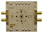
Figure 1. NB4L16MMN Evaluation PCB with Pin Label/Connection Change
© Semiconductor Components Industries, LLC, 2012
February, 2012 − Rev. 1
1
Publication Order Number:
EVBUM2069/D
�NB4L16MMNEVB
SETUP FOR TIME DOMAIN MEASUREMENTS
Table 1. BASIC EQUIPMENT
Example Equipment (Note 1)
Description
Qty.
Power Supply with 4 outputs
HP6624A
1
Oscilloscope
TDS8000 with 80E01 Sampling Head (Note 2)
1
Differential Signal Generator
HP 8133A, Advantest D3186
1
Matched High Speed Cables with SMA Connectors
Storm, Semflex
4
Power Supply Cables with Clips
8
1. Equipment used to generate example measurements within this document.
2. 50 GHz sampling head used (for effective rise, fall and jitter performance measurement)
Setup
Step 1: Connect Power
Step 2: Connect Inputs
1a: Two power levels must be provided to the board for
VCC and VEE via the surface mount clips.
For Differential Mode (3.3 V and 2.5 V operation)
2a: Connect the differential output of the generator to the
differential input of the device (D and D).
NOTE: Device may oscillate when the input is not
driven.
Table 2. NB4L16M Power Supply Connections
3.3 V Setup
2.5 V Setup
VCC = 0 V = GND
VCC = 0 V = GND
VTT = VCC = 0 V = GND
VEE = −3.3 V
VTT = VCC = 0 V = GND
VEE = −2.5 V
VCC = 0 V
Signal Generator
OUT
OUT
Amplitude = 500 mV
Offset = −250 mV
TRIGGER
NOTE:
VTT = 0 V
VCC
Digital Oscilloscope
GND
C1
D
Q
D
VBB
C1
VEE
Q
Channel 1
Channel 2
GND
VTT = 0 V
VEE = −3.3 V (3.3 V op)
VEE = −2.5 V (2.5 V op)
TRIGGER
All differential cable pairs must be matched.
Figure 2. NB4L16M Board Setup − Time Domain (Differential Mode)
http://onsemi.com
2
�NB4L16MMNEVB
Step 3: Setup Input Signals
3c: Set the generator output for a PRBS data signal, or for
a square wave clock signal with a 50% duty cycle.
3a: Set the signal generator amplitude to 500 mV.
NOTE: The signal generator amplitude can vary from
75 mV to 900 mV to produce a 400 mV DUT
output.
Step 4: Connect Output Signals
4a: Connect the outputs of the device (Q, Q) to the
oscilloscope. The oscilloscope sampling head must have
internal 50 W termination to ground.
NOTE: Where a single output is being used, the
unconnected output for the pair must be
terminated to VTT through a 50 W resistor for
best operation. Unused pairs may be left
unconnected. Since VTT = 0 V, a standard 50 W
SMA termination is recommended.
3b: Set the signal generator offset to −250 mV.
NOTE: The VIHCMR (Input High Voltage Common
Mode Range) allows the signal generator offset
to vary as long as VIH is within the VIHCMR
range. Refer to the device data sheet for further
information.
SETUP FOR FREQUENCY DOMAIN MEASUREMENTS
Table 3. BASIC EQUIPMENT
Example Equipment (Note 3)
Description
Qty
Power Supply with 4 outputs
HP 6624A
1
Vector Network Analyzer (VNA)
R&S ZVK (10 MHz to 40 GHz)
1
180° Hybrid Coupler
Krytar Model #4010180
1
Bias Tee with 50 W Resistor Termination
Picosecond Model #5542−219
1
Matched High Speed Cables with SMA Connectors
Storm, Semflex
3
Power Supply Cables with Clips
8
3. Equipment used to generate example measurements within this document.
Setup
Step 1: Connect Power
Setup Test Configurations for Differential Operation
1a:Two power levels must be provided to the board for
VCC and VEE via the surface mount clips.
Small Signal Setup
Step 2: Input Setup
Table 4. NB4L16M Power Supply Connections
2a: Calibrate VNA from 1.0 GHz to 12 GHz.
2b: Set input level to –35 dBm at the output of the 180°
Hybrid coupler (input of the DUT).
3.3 V Setup
VCC = 0 V = GND
VTT = VCC = 0 V = GND
Step 3: Output Setup
3a: Set display to measure S21 and record data.
VEE = −3.3 V
Large Signal Setup
Step 2: Input Setup
2a: Calibrate VNA from 1.0 GHz to 12 GHz.
2b: Set input levels to −2.0 dBm (500 mV) at the input of
DUT.
Step 3: Output Setup
3a: Set display to measure S21 and record data.
http://onsemi.com
3
�NB4L16MMNEVB
Vector Network Analyzer
PORT 1
Bias T
PORT 2
GND − 250 mV
VCC = 0 V
GND
VTT = 0 V
GND
50 W
VCC
GND
50 W
D
C1
Q
180� Hybrid
Coupler
D
VBB
GND
C1
VEE
Bias T
Q
GND
50 W
GND
VTT = 0 V
VEE = −3.3 V (3.3 V op)
Figure 3. Board Setup – Frequency Domain (Differential Mode)
http://onsemi.com
4
�NB4L16MMNEVB
MORE INFORMATION ABOUT EVALUATION BOARD
Design Considerations for >10 GHz operation
The following considerations played a key role to ensure
this evaluation board achieves high−end microwave
performance:
• Optimal SMA connector launch
• Minimal insertion loss and signal dispersion
• Accurate Transmission line matching (50 ohms)
• Distributed effects while bypassing and noise filtering
While the NB4L16M is specified to operate at 12 GHz,
this evaluation board is designed to support operating
frequencies up to 20 GHz.
SURFACE MOUNT CLIP
OPEN CIRCUIT STUB
T6
l/4 @ 10 GHz
T5
l/2 @ 10 GHz
T3
VCC
C1
0
VTD
0
ROSENBERGER SMA
ROSENBERGER SMA
1
1
T1
T1
Q
T2
D
1
ROSENBERGER SMA
NB4L16M
D
Q
T2
1
ROSENBERGER SMA
VTD
0
0
T5
l/2 @ 10 GHz
C1
T6
OPEN CIRCUIT STUB
T4
l/4 @ 10 GHz
VBB
VEE
SURFACE MOUNT CLIP
NOTE:
C1, C2* = Decoupling cap
Tx = 50 W Transmission line
Figure 4. Evaluation Board Schematic
http://onsemi.com
5
�NB4L16MMNEVB
Table 5. PARTS LIST
Part No
Qty
Description
Manufacturer
WEB address
NB4L16MMN
1
2.5 V/3.3 V, 5 Gb/s Multi Level
Clock/Data Input to CML Receiver/
Driver/ Translator with
Internal Termination
ON Semiconductor
http://www.onsemi.com
32K243−40ME3
4
Gold Plated Connector
Rosenberger
http://www.rosenberger.de
CO6BLBB2X5CO6
03CL04K6RAC
9
2 MHz – 30 GHz Capacitor
0603 0.1 mF $10%
Dielectric Laboratories
Kemet
http://www.dilabs.com
http://www.newark.com/
SO16
9
Test Point−Anvil
Keystone
http://www.newark.com
http://www.digikey.com
Table 6. BOARD MATERIAL
Material
Thickness
Rogers 6002
5 mil
Copper Plating
32 mil
PIN 1
12.5 mil
1.37 mil
Dielectric (5.0 mil)
Thick Copper Base
Figure 5. Board Stack−up
Figure 6. Layout Mask for NB4L16M
11 GHz
1 dB/div
5 dB
START 1 GHz
NOTE:
1 GHz/
H
STOP 12 GHz
The insertion loss curve can be used to calibrate out board loss if testing
under small signal conditions.
Figure 7. Insertion Loss
http://onsemi.com
6
�NB4L16MMNEVB
ADDITIONAL EVALUATION BOARD INFORMATION
www.onsemi.com
References
In all cases, the most up−to−date information can be found
on our website.
• Sample orders for devices and boards
• New Product updates
• Literature download/order
• IBIS and Spice models
NB4L16M/D, Data Sheet, 2.5V/3.3V, 5 Gb/s Multi Level
Clock/Data Input to CML Driver / Receiver /
Buffer / Translator with Internal Termination
AND8077/D, Application Note, GigaComm] (SiGe)
SPICE Modeling Kit.
AND8075/D, Application Note, Board Mounting
Considerations for the FCBGA Packages.
ORDERING INFORMATION
Package
Shipping
NB4L16MMN
Part No
2.5V/3.3V, 5 Gb/s Multi Level Clock/Data Input to CML
Driver / Receiver / Buffer / Translator with Internal Termination
Description
3X3 mm
QFN−16
123 Units/Tray
NB4L16MMNG
2.5V/3.3V, 5 Gb/s Multi Level Clock/Data Input to CML
Driver / Receiver / Buffer / Translator with Internal Termination
3X3 mm
QFN−16
(Pb−Free)
123 Units/Tray
NB4L16MMNR2
2.5V/3.3V, 5 Gb/s Multi Level Clock/Data Input to CML
Driver / Receiver / Buffer / Translator with Internal Termination
3X3 mm
QFN−16
3000 / Tape & Reel
NB4L16MMNEVB
NB4L16MN Evaluation Board
†For information on tape and reel specifications, including part orientation and tape sizes, please refer to our Tape and Reel Packaging
Specifications Brochure, BRD8011/D.
http://onsemi.com
7
�NB4L16MMNEVB
PACKAGE DIMENSIONS
16 PIN QFN
MN SUFFIX
CASE 485G−01
ISSUE B
D
PIN 1
LOCATION
ÇÇÇ
ÇÇÇ
ÇÇÇ
0.15 C
NOTES:
1. DIMENSIONING AND TOLERANCING PER
ASME Y14.5M, 1994.
2. CONTROLLING DIMENSION: MILLIMETERS.
3. DIMENSION b APPLIES TO PLATED
TERMINAL AND IS MEASURED BETWEEN
0.25 AND 0.30 MM FROM TERMINAL.
4. COPLANARITY APPLIES TO THE EXPOSED
PAD AS WELL AS THE TERMINALS.
5. Lmax CONDITION CAN NOT VIOLATE 0.2 MM
MINIMUM SPACING BETWEEN LEAD TIP
AND FLAG
A
B
E
DIM
A
A1
A3
b
D
D2
E
E2
e
K
L
TOP VIEW
0.15 C
(A3)
0.10 C
A
16 X
SEATING
PLANE
0.08 C
SIDE VIEW
A1
C
D2
16X
L
5
NOTE 5
e
4
16X
9
E2
K
12
1
16
16X
e
13
b
0.10 C A B
0.05 C
EXPOSED PAD
8
BOTTOM VIEW
NOTE 3
GigaComm is a trademark of Semiconductor Components Industries, LLC.
http://onsemi.com
8
MILLIMETERS
MIN
MAX
0.80
1.00
0.00
0.05
0.20 REF
0.18
0.30
3.00 BSC
1.65
1.85
3.00 BSC
1.65
1.85
0.50 BSC
0.20
−−−
0.30
0.50
�onsemi,
, and other names, marks, and brands are registered and/or common law trademarks of Semiconductor Components Industries, LLC dba “onsemi” or its affiliates
and/or subsidiaries in the United States and/or other countries. onsemi owns the rights to a number of patents, trademarks, copyrights, trade secrets, and other intellectual property. A
listing of onsemi’s product/patent coverage may be accessed at www.onsemi.com/site/pdf/Patent−Marking.pdf. onsemi is an Equal Opportunity/Affirmative Action Employer. This
literature is subject to all applicable copyright laws and is not for resale in any manner.
The evaluation board/kit (research and development board/kit) (hereinafter the “board”) is not a finished product and is not available for sale to consumers. The board is only intended
for research, development, demonstration and evaluation purposes and will only be used in laboratory/development areas by persons with an engineering/technical training and familiar
with the risks associated with handling electrical/mechanical components, systems and subsystems. This person assumes full responsibility/liability for proper and safe handling. Any
other use, resale or redistribution for any other purpose is strictly prohibited.
THE BOARD IS PROVIDED BY ONSEMI TO YOU “AS IS” AND WITHOUT ANY REPRESENTATIONS OR WARRANTIES WHATSOEVER. WITHOUT LIMITING THE FOREGOING,
ONSEMI (AND ITS LICENSORS/SUPPLIERS) HEREBY DISCLAIMS ANY AND ALL REPRESENTATIONS AND WARRANTIES IN RELATION TO THE BOARD, ANY
MODIFICATIONS, OR THIS AGREEMENT, WHETHER EXPRESS, IMPLIED, STATUTORY OR OTHERWISE, INCLUDING WITHOUT LIMITATION ANY AND ALL
REPRESENTATIONS AND WARRANTIES OF MERCHANTABILITY, FITNESS FOR A PARTICULAR PURPOSE, TITLE, NON−INFRINGEMENT, AND THOSE ARISING FROM A
COURSE OF DEALING, TRADE USAGE, TRADE CUSTOM OR TRADE PRACTICE.
onsemi reserves the right to make changes without further notice to any board.
You are responsible for determining whether the board will be suitable for your intended use or application or will achieve your intended results. Prior to using or distributing any systems
that have been evaluated, designed or tested using the board, you agree to test and validate your design to confirm the functionality for your application. Any technical, applications or
design information or advice, quality characterization, reliability data or other services provided by onsemi shall not constitute any representation or warranty by onsemi, and no additional
obligations or liabilities shall arise from onsemi having provided such information or services.
onsemi products including the boards are not designed, intended, or authorized for use in life support systems, or any FDA Class 3 medical devices or medical devices with a similar
or equivalent classification in a foreign jurisdiction, or any devices intended for implantation in the human body. You agree to indemnify, defend and hold harmless onsemi, its directors,
officers, employees, representatives, agents, subsidiaries, affiliates, distributors, and assigns, against any and all liabilities, losses, costs, damages, judgments, and expenses, arising
out of any claim, demand, investigation, lawsuit, regulatory action or cause of action arising out of or associated with any unauthorized use, even if such claim alleges that onsemi was
negligent regarding the design or manufacture of any products and/or the board.
This evaluation board/kit does not fall within the scope of the European Union directives regarding electromagnetic compatibility, restricted substances (RoHS), recycling (WEEE), FCC,
CE or UL, and may not meet the technical requirements of these or other related directives.
FCC WARNING – This evaluation board/kit is intended for use for engineering development, demonstration, or evaluation purposes only and is not considered by onsemi to be a finished
end product fit for general consumer use. It may generate, use, or radiate radio frequency energy and has not been tested for compliance with the limits of computing devices pursuant
to part 15 of FCC rules, which are designed to provide reasonable protection against radio frequency interference. Operation of this equipment may cause interference with radio
communications, in which case the user shall be responsible, at its expense, to take whatever measures may be required to correct this interference.
onsemi does not convey any license under its patent rights nor the rights of others.
LIMITATIONS OF LIABILITY: onsemi shall not be liable for any special, consequential, incidental, indirect or punitive damages, including, but not limited to the costs of requalification,
delay, loss of profits or goodwill, arising out of or in connection with the board, even if onsemi is advised of the possibility of such damages. In no event shall onsemi’s aggregate liability
from any obligation arising out of or in connection with the board, under any theory of liability, exceed the purchase price paid for the board, if any.
The board is provided to you subject to the license and other terms per onsemi’s standard terms and conditions of sale. For more information and documentation, please visit
www.onsemi.com.
PUBLICATION ORDERING INFORMATION
LITERATURE FULFILLMENT:
Email Requests to: orderlit@onsemi.com
onsemi Website: www.onsemi.com
◊
TECHNICAL SUPPORT
North American Technical Support:
Voice Mail: 1 800−282−9855 Toll Free USA/Canada
Phone: 011 421 33 790 2910
www.onsemi.com
1
Europe, Middle East and Africa Technical Support:
Phone: 00421 33 790 2910
For additional information, please contact your local Sales Representative
�


 工商网监
湘ICP备2023018690号
工商网监
湘ICP备2023018690号
