NB4N840MMNEVB
Evaluation Board User's
Manual for NB4N840M
http://onsemi.com
EVAL BOARD USER’S MANUAL
Description
applications. Each 2 x 2 crosspoint switch can fan−out
and/or multiplex up to 3.2 Gb/s data and 2.7 GHz clock
signals.
Internally terminated differential CML inputs accept
AC−coupled LVPECL (Positive ECL) or direct coupled
CML signals. By providing internal 50 W input and output
termination resistor, the need for external components is
eliminated and interface reflections are minimized.
Differential 16 mA CML outputs provide matching internal
50 W terminations, and 400 mV output swings when
externally terminated, 50 W to VCC.
Single−ended LVCMOS/LVTTL SEL inputs control the
routing of the signals through the crosspoint switch which
makes this device configurable as 1:2 fan−out, repeater or
2 x 2 crosspoint switch. The device is housed in a low profile
5 x 5 mm 32−pin QFN package.
The NB4N840M Evaluation Board was designed to
provide a flexible and convenient platform to quickly
evaluate, characterize and verify the performance and
operation of the NB4N840M dual 2 x 2 Crosspoint Switch.
This user’s manual provides detailed information on the
board’s contents, layout and use. The manual should be used
in conjunction with the NB4N840M data sheet which
contains full technical details on device specifications and
operation.
The NB4N840M is a high−bandwidth fully differential
dual 2 x 2 crosspoint switch with CML inputs/outputs that
is suitable for applications such as SDH/SONET DWDM
and high speed switching. Fully differential design
techniques are used to minimize jitter accumulation,
crosstalk, and signal skew, which make this device ideal for
loop−through and protection channel switching
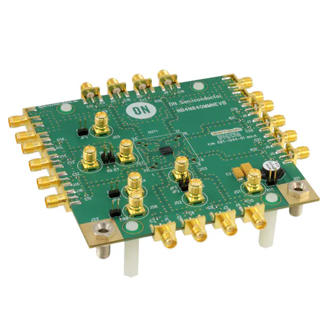
Figure 1. NB4N840M Evaluation Board
© Semiconductor Components Industries, LLC, 2012
February, 2012 − Rev. 2
1
Publication Order Number:
EVBUM2078/D
�NB4N840MMNEVB
Board Features
Power Supply
• Fully assembled evaluation board
• Accommodates the electrical characterization of the
•
•
•
NB4N840M in the QFN32 package
Equal length input and output data lines to minimize
skew
Selectable jumpers
Single + 3.3 V supply
+
Figure 2. Power Supply Connections
Step 3: Input Connections
DAn and DBn require CML drive levels and provide
internal 50 W to VCC termination resistors to eliminate
external components and minimize reflections. Ensure that
the CML devices driving these inputs are not redundantly
terminated.
Step 1: Basic Equipment
Signal Generator
Oscilloscope
Power Supply
Voltmeter
Matched High−Speed Cables with SMA Connectors
Table 2. Input Connectors
Step 2: Power Supply Connections
+ 3.3 V must be provided to the board for VCC.
Table 1. Power Supply Connections
Supply
Value
Connector
VCC
+ 3.3 V
J21
GND
0V
J22
GND
+3.3 V
Information on the NB4N840M Evaluation Board
Appropriate Lab Setup Details
Evaluation Board Layout
Bill of Materials
Setup for Measurements
•
•
•
•
•
−
VCC
This Evaluation Board Manual Contains
•
•
•
•
+3.3 V
Inputs
Board Connector
DA0
J13
DA0
J14
DA1
J15
DA1
J16
DB0
J3
DB0
J4
DB1
J1
DB1
J2
Step 4: Control and Select Pins
Jumpers JP1, JP2, JP5, and JP6 select the input signals for channel A and B outputs. Jumpers JP3, JP4, JP7, and JP8 enable
the output drivers for channel A and B (refer to Table 3 for output routing).
Table 3. Output Routing
ROUTING CONTROLS
OUTPUT CONTROLS
OUTPUT SIGNALS
SELA0 / SELB0
SELA1 / SELB1
ENA0 / ENA1
ENB0 / ENB1
JP6 / JP2
JP5 / JP1
JP7 / JP8
JP3 / JP4
Signal at
QA0 / QB0
Signal at
QA1 / QB1
L
L
H
H
DA0 / DB0
DA0 / DB0
L
H
H
H
DA0 / DB0
DA1 / DB1
H
L
H
H
DA1 / DB1
DA0 / DB0
H
H
H
H
DA1 / DB1
DA1 / DB1
X
X
L
L
Power Down
Power Down
http://onsemi.com
2
�NB4N840MMNEVB
(J13) DA0
(J14) DA0
(J15) DA1
(J16) DA1
(J3) DB0
(J4) DB0
CML
0
1
0
CML
0
CML
1
0
(J1) DB1
(J2) DB1
QA0
(J11)
ENA0
(JP7)
SELA0
(JP6)
QA1
(J10)
QA1
(J9)
ENA1
(JP8)
SELA1
(JP5)
QB0
(J6)
QB0
(J5)
ENB0
(JP3)
SELB0
(JP2)
QB1
(J8)
QB1
(J7)
ENB1
(JP4)
SELB1
(JP1)
CML
1
CML
(J12)
CML
1
CML
QA0
CML
Figure 3. NB4N840M Evaluation Board Connector Configuration
Step 5: Output Connections
2. Monitoring CML Outputs with High−Impedance
Oscilloscope Inputs
The CML outputs, QAn and QBn, must be AC−coupled
to a 50 W termination (100 W differential) load. On−board
100−W differential terminations are provided to reduce
noise on outputs that are not used. Connect the QAn/QBn
CML outputs to the oscilloscope with equally matched
cables.
a. Leave the coupling capacitors in series with the
outputs.
b. Make sure the differential load resistors are on all the
outputs (R9–R12).
1. Monitoring One or More CML Outputs with 50 W
Oscilloscope Inputs
Table 4. Output Connectors
a. Leave the coupling capacitors in series with the
outputs.
b. Remove the associated 100 W differential load
resistors from the evaluation board on the outputs
(R9–R12).
c. It is important to remove the 100 W resistor on the
output monitored, otherwise the load impedance will
not match the characteristic impedance of the line
and the resulting reflections will cause a degradation
in the output signal quality.
d. If you are observing a single−ended output, balance
the other half with a 50 W termination to ground
(through the AC−coupling capacitor).
http://onsemi.com
3
Outputs
Board Connector
QA0
J12
QA0
J11
QA1
J10
QA1
J9
QB0
J6
QB0
J5
QB1
J8
QB1
J7
�NB4N840MMNEVB
VCC
C3
0.1 mF
C4
0.1 mF
C5
0.1 mF
C6
0.1 mF
VCC
L1
4.7 mH
C23
0.1 mF
C1
33 mF
C24
0.1 mF
C2
2.2 mF
vcc
C11
0.1 mF
JP8
JP7
JP6
JP5
0.1 mF
4
JP3
J3
6
C9
0.1 mF
JP1
8
J4
C10
0.1 mF
R1 R2
R3
1 kW 1 kW 1 kW
7
SELA1
DA0
DA0
SELA0
ENA0
GND
VCC
DB1
QA0
DB1
ENB0
QA0
NB4N840M
SELB0
VCC
DB0
QA1
DB0
QA1
SELB1
VCC
9
R4
1 kW
10
11
12
VCC
13
14
C21
0.1 mF
1
2
1
J6
C20
0.1 mF
2
Figure 4. Evaluation Board Schematic
http://onsemi.com
4
VCC
22
21
20
1
R9
100 W
C16
0.1 mF
C17
0.1 mF
19
1
18
R10
100 W
17
VCC
2
J11
1
VCC
2
J8
2
23
J12
C18
0.1 mF
1
2
J10
2
J9
2
1
C29
C31
0.1 mF 0.1 mF J18
1
2
C19
C30
C27
0.1 mF
J19 0.1 mF 0.1 mF J20
1
1
1
1
J7
C15
0.1 mF
24
J17
R11
100 W
C22
0.1 mF
J13
16
VCC
R12
100 W
J5
15
VCC
J15
25 C14
26
ENB1
GND
JP2
5
27
VCC
3
28
QB1
2
29
QB1
J2
C8
0.1 mF
1
30
VCC
JP4
VCC
C7
0.1 mF
ENA1
J1
31
DA1
32
C12
J14
0.1 mF C13
R5
1 kW
QB0
R6
1 kW
DA1
R7
1 kW
QB0
R8
1 kW
0.1 mF
J16
2
2
2
�NB4N840MMNEVB
Table 5. BILL OF MATERIALS
Ref. Number
Qty
Description
Manufacturer Part No.
(Notes 1, 2)
Manufacturer
R1 – R8
8
1 kW ±1%, 0402, Resistors
Multicomp
MC0402WGF1001TCE−TR
R9 – R12
4
100 W ±1%, 0402, Resistors
Multicomp
MC0402WGF1000TCE−TR
C1
1
33 mF ±10%, size “D”, Tantalum Capacitor
Kemet
T491D336K016AT
C2
1
2.2 mF ±10%, size “C”, Tantalum Capacitor
Kemet
T491C225K035AT
C3 – C24, C27,
C29 – C31
26
0.1 mF ±10%, 0402, Ceramic Capacitors
Kemet
C0402C104K4RAC−TU
L1
1
4.7 mH Inductor
Coilcraft
DT3316P−472MLB
U1
1
32 pin QFN
ON Semiconductor
NB4N840MMNG
J1 – J20
20
SMA Edge Mount Connectors
Johnson
142−0701−851
JS1 – JS8
8
SMA Connectors
Johnson
142−0701−201
J21, J22
2
Test Point Jacks
JP1 – JP8
8
1x2 Pin Headers, (0.1 inch pitch)
SPC
SPC20485
JP1 – JP8
8
Shunts
SPC
SPC19809
1. Specified parts are RoHS−compliant.
2. Only RoHS−compliant equivalent parts may be substituted.
Board Lay−Up
This board is implemented in four layers and provides a high bandwidth 50 W controlled impedance environment. The
pictures in Figures 5 through 9 show views of the four layers of the evaluation board. Board material is FR4.
Top Silkscreen
Top Soldermask
Top Plating
01
Cu = 1/2 oz, 0.0007
Top Metal
0.062 ± 0.010
Dielectric 0.014
02
Cu = 1/2 oz, 0.0007
Plane
Adjust
03
Cu = 1/2 oz, 0.0007
Plane
Dielectric 0.014
04
Cu = 1/2 oz, 0.0007
Bottom Plating
Bottom Soldermask
Bottom Silkscreen
Figure 5. Evaluation Board Lay−Up
http://onsemi.com
5
Bottom Metal
�NB4N840MMNEVB
Figure 6. NB4N840MMN Evaluation Board Top (Component) Layer
Figure 7. Ground Layer
http://onsemi.com
6
�NB4N840MMNEVB
Figure 8. Power Layer
Figure 9. Bottom Layer
http://onsemi.com
7
�onsemi,
, and other names, marks, and brands are registered and/or common law trademarks of Semiconductor Components Industries, LLC dba “onsemi” or its affiliates
and/or subsidiaries in the United States and/or other countries. onsemi owns the rights to a number of patents, trademarks, copyrights, trade secrets, and other intellectual property. A
listing of onsemi’s product/patent coverage may be accessed at www.onsemi.com/site/pdf/Patent−Marking.pdf. onsemi is an Equal Opportunity/Affirmative Action Employer. This
literature is subject to all applicable copyright laws and is not for resale in any manner.
The evaluation board/kit (research and development board/kit) (hereinafter the “board”) is not a finished product and is not available for sale to consumers. The board is only intended
for research, development, demonstration and evaluation purposes and will only be used in laboratory/development areas by persons with an engineering/technical training and familiar
with the risks associated with handling electrical/mechanical components, systems and subsystems. This person assumes full responsibility/liability for proper and safe handling. Any
other use, resale or redistribution for any other purpose is strictly prohibited.
THE BOARD IS PROVIDED BY ONSEMI TO YOU “AS IS” AND WITHOUT ANY REPRESENTATIONS OR WARRANTIES WHATSOEVER. WITHOUT LIMITING THE FOREGOING,
ONSEMI (AND ITS LICENSORS/SUPPLIERS) HEREBY DISCLAIMS ANY AND ALL REPRESENTATIONS AND WARRANTIES IN RELATION TO THE BOARD, ANY
MODIFICATIONS, OR THIS AGREEMENT, WHETHER EXPRESS, IMPLIED, STATUTORY OR OTHERWISE, INCLUDING WITHOUT LIMITATION ANY AND ALL
REPRESENTATIONS AND WARRANTIES OF MERCHANTABILITY, FITNESS FOR A PARTICULAR PURPOSE, TITLE, NON−INFRINGEMENT, AND THOSE ARISING FROM A
COURSE OF DEALING, TRADE USAGE, TRADE CUSTOM OR TRADE PRACTICE.
onsemi reserves the right to make changes without further notice to any board.
You are responsible for determining whether the board will be suitable for your intended use or application or will achieve your intended results. Prior to using or distributing any systems
that have been evaluated, designed or tested using the board, you agree to test and validate your design to confirm the functionality for your application. Any technical, applications or
design information or advice, quality characterization, reliability data or other services provided by onsemi shall not constitute any representation or warranty by onsemi, and no additional
obligations or liabilities shall arise from onsemi having provided such information or services.
onsemi products including the boards are not designed, intended, or authorized for use in life support systems, or any FDA Class 3 medical devices or medical devices with a similar
or equivalent classification in a foreign jurisdiction, or any devices intended for implantation in the human body. You agree to indemnify, defend and hold harmless onsemi, its directors,
officers, employees, representatives, agents, subsidiaries, affiliates, distributors, and assigns, against any and all liabilities, losses, costs, damages, judgments, and expenses, arising
out of any claim, demand, investigation, lawsuit, regulatory action or cause of action arising out of or associated with any unauthorized use, even if such claim alleges that onsemi was
negligent regarding the design or manufacture of any products and/or the board.
This evaluation board/kit does not fall within the scope of the European Union directives regarding electromagnetic compatibility, restricted substances (RoHS), recycling (WEEE), FCC,
CE or UL, and may not meet the technical requirements of these or other related directives.
FCC WARNING – This evaluation board/kit is intended for use for engineering development, demonstration, or evaluation purposes only and is not considered by onsemi to be a finished
end product fit for general consumer use. It may generate, use, or radiate radio frequency energy and has not been tested for compliance with the limits of computing devices pursuant
to part 15 of FCC rules, which are designed to provide reasonable protection against radio frequency interference. Operation of this equipment may cause interference with radio
communications, in which case the user shall be responsible, at its expense, to take whatever measures may be required to correct this interference.
onsemi does not convey any license under its patent rights nor the rights of others.
LIMITATIONS OF LIABILITY: onsemi shall not be liable for any special, consequential, incidental, indirect or punitive damages, including, but not limited to the costs of requalification,
delay, loss of profits or goodwill, arising out of or in connection with the board, even if onsemi is advised of the possibility of such damages. In no event shall onsemi’s aggregate liability
from any obligation arising out of or in connection with the board, under any theory of liability, exceed the purchase price paid for the board, if any.
The board is provided to you subject to the license and other terms per onsemi’s standard terms and conditions of sale. For more information and documentation, please visit
www.onsemi.com.
PUBLICATION ORDERING INFORMATION
LITERATURE FULFILLMENT:
Email Requests to: orderlit@onsemi.com
onsemi Website: www.onsemi.com
◊
TECHNICAL SUPPORT
North American Technical Support:
Voice Mail: 1 800−282−9855 Toll Free USA/Canada
Phone: 011 421 33 790 2910
www.onsemi.com
1
Europe, Middle East and Africa Technical Support:
Phone: 00421 33 790 2910
For additional information, please contact your local Sales Representative
�


 工商网监
湘ICP备2023018690号
工商网监
湘ICP备2023018690号
