NB6L295MNGEVB,
NB6L295MMNGEVB
NB6L295MNG/
NB6L295MMNG Evaluation
Board User's Manual
http://onsemi.com
EVAL BOARD USER’S MANUAL
Introduction and Board Description
The NB6L295M Evaluation Board was designed to
provide a flexible and convenient platform to quickly
evaluate, characterize and verify the operation and
performance of either the NB6L295MMNG (CML) or the
NB6L295MNG (LVPECL) Dual Channel Programmable
Delay.
This evaluation board manual contains:
• Information on the NB6L295M Evaluation Board
• Appropriate Lab Setup
• Detailed Board Features
• Bill of Materials
This manual should be used in conjunction with the device
datasheet NB6L295M/D or NB6L295/D which contains full
technical details on the device specifications and operation.
The NB6L295M Evaluation Board was also designed to
accommodate a custom QFN−24 socket. Therefore, some
external components were installed on the bottom side of the
board.
• SMA connectors are provided for 1) all high−speed
Board Features
With this evaluation board, the following measurements
could be performed in single ended or differential modes of
operation.
• Propagation and Programmed Delay
• Output Rise and Fall Time
• Frequency Performance
• Jitter
• VCMR − Common Mode Range
differential input & (CML or LVPECL) output signals
and 2) for external SDI & control signals access
Board Layout
The evaluation board is constructed in four layers. The top
layer is the primary trace layer and is made with polyimide
material. This layer provides a high−bandwidth 50 W
controlled trace impedance environment for the equal length
inputs and outputs. The second layer is a copper ground
plane.
Layer Stack
L1 Signal − “High and Low Speed”
L2 SMA Ground
L3 VCC (Device positive power supply) and DUTGND
(Device negative power supply)
L4 Signal − “Low Speed”
What measurements can you expect to make?
• On board programmable SDI circuitry minimizing
•
•
•
cabling, or, external SDI accessed through SMA
connectors.
Convenient and compact board layout
2.5 V or 3.3 V single or split−power supply operation
(banana jack connectors for VCC, SMAGND and
DUTGND; Separate PLDVCC power supply for on
board PLD
CML or LVPECL differential output signals are
accessed via SMA connectors with provision for load
termination resistors
© Semiconductor Components Industries, LLC, 2012
April, 2012− Rev. 3
1
Publication Order Number:
EVBUM2082/D
�NB6L295MNGEVB, NB6L295MMNGEVB
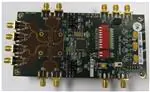
Figure 1. NB6L295MNGEVB Evaluation Board Photo
Figure 2. NB6L295MMNGEVB Evaluation Board Photo
http://onsemi.com
2
�NB6L295MNGEVB, NB6L295MMNGEVB
DUTGND = PLDGND
D
U
T
G
N
D
S
M
A
G
N
D
D
U
T
V
C
C
P
L
D
V
C
C
On−Board SDI
Control for 11−Bit
Delay Register
Push Button to
Load Selected Dx
Delay Bits
External Control
Inputs for SDI
PLD for SDI
Control
Data / Clock IN1
PD1
PD0
Q1
Q0
Figure 3. NB6L295M Evaluation Board Layout Overview
http://onsemi.com
3
Data / Clock IN0
�NB6L295MNGEVB, NB6L295MMNGEVB
TEST AND MEASUREMENT SETUP AND PROCEDURE
Basic Lab Equipment (or Equivalent)
Dual Power Supplies
• Agilent Signal Generator #8133A for INx / INx,
•
•
•
•
external Clock or Data source
Tektronix TDS8000 Oscilloscope or Frequency Counter
Agilent #6624A DC Power Supply
Digital Voltmeter
Matched high−speed cables with SMA connectors
0V
+2.5 V
+
−
+
−
DUTGND
VCC
SMAGND
Lab Setup
A typical lab setup for taking time domain measurements
in differential mode operation is shown in Figures 6 and 7.
The following steps should be followed for proper
equipment setup:
+2.5 V
Figure 4. “Split” or Dual Power Supply Connections
for NB6L295M, CML Outputs
Step 1: Connect Power Supply
The NB6L295M and NB6L295 have positive supply pins,
VCC, VCC0 and VCC1, and negative supply pins,
(DUT)GND. The SMAGND (VTT) terminal is the isolated
termination ground plane for the outputs, only, and is not to
be confused with the device ground pin, (DUT)GND.
Three power levels must be provided to the board, VCC,
DUTGND, and SMAGND. Connect a power supplies to
banana jack connectors for VCC, PLDVCC, DUTGND and
SMAGND, which are provided on the bottom of the board.
By−pass capacitors have been installed from VCC to
SMAGND and from DUTGND to SMAGND at the banana
jacks.
DUTGND = PLDGND, therefore, when device power
supply is 2.5 V or 3.3 V, PLDVCC = DUTVCC. The
exposed pad on the PCB for the QFN−24 package is
connected to DUTGND.
Table 1. NB6L295M, CML OUTPUTS OFFSET POWER
SUPPLY CONFIGURATIONS
Dual Power Supplies
2.0 V
+
VCC
Device Pin
Power Supply
Connector
Color
“Spilt” Power Supply
PLDVCC
Yellow
PLDVCC = 0 V
VCC
Red
VCC = 0 V
SMAGND
Black
VTT = 0 V
DUTGND
Black
DUTGND = −2.5 V or −3.3 V
Table 2. NB6L295, LVPECL OUTPUTS “SPLIT”
POWER SUPPLY CONFIGURATIONS
Device Pin
Power Supply
Connector
Color
“Spilt” Power Supply
PLDVCC
Yellow
PLDVCC = +2.0 V
VCC
Red
VCC = +2.0 V
SMAGND
Black
VTT = 0 V
DUTGND
Black
DUTGND = −0.5 V or −1.3 V
+1.3 V
−
+
−
DUTGND
SMAGND
+3.3 V
Figure 5. “Split” or Dual Power Supply Connections
for NB6L295, LVPECL Outputs
http://onsemi.com
4
�NB6L295MNGEVB, NB6L295MMNGEVB
Step 2: CML & LVPECL Output Load Termination
Step 4: Program the SDI
The internal delay registers of the NB6L295/NB6L295M
may be programmed by a) the onboard PLD or b) by using
the three−lines for an external Serial Data Interface (SDI)
consisting of a SERIAL DATA (SDATA) input, a SERIAL
CLOCK (SCLK) input, and a SERIAL LOAD (SLOAD) as
follows:
a) Onboard PLD
When using the onboard PLD for the SDI source,
1. Install the three jumpers located at J4
2. Insure PLDVCC power is applied
3. The 11−bit switches will program the NB6L295’s
11−bit shift register. Set SW2 and SW4 switches to
the desired values for the 11−bit word
4. Load the program values by depressing
momentary switch SW3, or send a pulse signal
(125 ns min) through J1.
Refer to the NB6L295 datasheet for details on the proper
settings for these switches.
b. External SDI
An external SDI source can also program the
NB6L295/NB6L295M. See datasheet DC Table, AC Table,
as well as Figures 7 and 8. When using an external SDI
source, remove the three jumpers at J4.
To use the SDI ports, generate input SCLK, SDATA, and
SLOAD signals via the appropriate SMA connectors with
OFFSET LVCMOS/LVTTL LEVELS, i.e. +2.0 V HIGH
and −1.3 V LOW for a 3.3 V LVPECL power supply. The
SCLK signal will sample the information presented on
SDATA line. Values are loaded and indexed into a 11−bit
shift register. The register shifts once per rising edge of the
SCLK input. The serial input SDATA bits must each meet
setup and hold timing to the respective SCLK rising edge as
specified in the AC Characteristics section of the datasheet
document. The LEAST Significant Bit (LSB), PSEL, is
indexed in first followed by MSEL and D0, D1, D2, D3, D4,
D5, D6, and D7, through MOST Significant Bit (MSB), D8,
indexed in last. A Pulse on the SLOAD pin after the SHIFT
register is fully indexed (11 clocks) will load and latch the
data values for the internal registers.
The SLOAD pulse Low to HIGH rising edge transition
transfers the data from the SHIFT register to the LATCH
register. The SLOAD Pulse HIGH to LOW transition will
lock the new data values into the LATCH register.
After the PLD programs the NB6L295/NB6L295M,
PLDVCC can be disconnected.
Input/Output Enable −EN: When switch SW1 is in the UP
position or is externally connected to a LOW through J15
SMA connector, the outputs are ENABLED.
To monitor the Qx and Qx outputs on an oscilloscope or
frequency counter:
• The power supply needs to be DC offset
• Assure that the instrument has internal 50 W
termination impedance to ground
• Ensure the oscilloscope is triggered properly
NB6L295M − CML Outputs (see Figures 4 and 7)
The CML Qx and Qx outputs must be externally DC
loaded and AC terminated. A “split” or dual power supply
technique can be used to take advantage of terminating the
CML outputs into 50 W to Ground of an oscilloscope or a
frequency counter. Since VTT = VCC, offsetting VCC to 0 V
yields VTT = 0 V or Ground (SMAGND).
NB6L295 − LVPECL Outputs (see Figures 5 and 6)
The LVPECL Qx and Qx outputs have standard, open
emitter outputs and must be externally DC loaded and AC
terminated.
Taking advantage of the internal 50 W to ground of the test
equipment, a split power supply technique will assure the
equal output loading and termination of both outputs.
Connect the Qx and Qx outputs of the device to the
oscilloscope with equally matched cables. Both outputs
must be equally loaded and terminated. The outputs are now
DC loaded and AC terminated with 50 W to VTT, which is
the Ground internal to the oscilloscope. Since VTT = VCC −
2 V, offsetting VCC to +2.0 V yields VTT = 0 V or Ground
(SMAGND).
The VTT terminal connects to the isolated SMAGND
connector ground plane, and is not to be confused with the
device ground pin, DUTGND.
NOTE: When a single−ended output is being used, the
unconnected output for the pair must be
terminated to VTT through a 50 W resistor for
best operation. Unused output pairs may be left
unconnected. Since VTT = 0 V, a standard 50 W
SMA termination plug can be used.
Step 3: Connect and Setup Inputs
Set the signal generator amplitude to appropriate logic levels
For Clock, set the generator output for a square wave clock
signal with a 50% duty cycle.
For Differential Mode
Connect the differential outputs of the generator with
equally matched cables to the differential inputs of the
device (INx and INx). The differential inputs of the
NB6L295 incorporate internal 50 W termination resistors.
For Single−Ended Mode
Connect the single−ended output of the generator to the
INx input of the device. Vth must be applied to the
complementary input (INx) when operating in single−ended
mode. Refer to the device datasheet for details on
single−ended operation.
The VTx and VTx termination pins each have a trace from
package pin to a node where it can be connected to either
VCC, DUTGND or SMAGND, depending on the user’s
need.
http://onsemi.com
5
�NB6L295MNGEVB, NB6L295MMNGEVB
DUTGND = −0.5 V / −1.3 V
SMAGND = 0 V VCC = +2.0 V
PLDVCC = +2.0 V
Signal
Generator
Signal Generator
IN0
IN1
IN0
IN1
Trigger
Trigger
Q0
Digital Oscilloscope or
Frequency Counter
50 W
Q0
50 W
Q1
Q1
50 W
50 W
Figure 6. Offset Power Supply Connections
for LVPECL Outputs, NB6L295
http://onsemi.com
6
Trigger
50 W
�NB6L295MNGEVB, NB6L295MMNGEVB
DUTGND = −2.5 V / −3.3 V
SMAGND = 0 V VCC = 0 V
PLDVCC = 0 V
Signal
Generator
Signal Generator
IN1
IN0
IN1
IN0
Trigger
Trigger
Q0
Digital Oscilloscope or
Frequency Counter
50 W
Q0
50 W
Q1
Q1
50 W
50 W
Figure 7. Offset Power Supply Connections
for CML Outputs, NB6L295M
http://onsemi.com
7
Trigger
50 W
�http://onsemi.com
8
A
B
PLD_SDATA
PLD_SCLK
J1
/IN1
IN1
IN0
/IN0
5
SMA_GND
VT1_
IN1_
VT1
VT0
IN0
IN0_
VT0_
EN_
J9
SW1
IN1
/EN
3
1
/EN 4
2
6
J4
6-pin Header
DUT_SDIN
DUT_SCLK
4
10
9
8
7
24
23
22
21
4
U6
NB6L295M
DUT_GND
25
EP
VT1_
IN1_
IN1
VT1
VT0
IN0
IN0_
VT0_
5 SLOAD
SCLK
4
SDIN
2
EN_
3
DUT_SLOAD
J8
SMA_GND
J7
J6
SMA_GND
J5
TP1
DUTVCC
DUT_GND
SMA_GND
J3
SMA_GND
J2
SMA_GND
/EN
SDIN
SCLK
C PLD_SLOAD
D
SLOAD
1
3
5
SLOAD 2
SCLK 4
SDIN 6
5
6
1
17
EP
EP
EP
EP
6
5
4
3
2
1
IN1_
VT1
IN1
Q1_
Q1
Q0_
Q0
DUT_GND
20
GND
GND 11
Q1_
13
12
VCC1
VCC1 15
14
Q1
Q0_
19
VCC0 16
VCC0
18
Q0
VCC
VCC
6
5
4
3
2
1
25
DUTVCC
DUT_GND
26
27
28
EN_
DUTVCC
DUT_GND
VT0
IN0
VT0_
14 14
13
13
17 17
16
16
15 15
3
Q0
DUT_GND
R3
DNI
SG3
Solder Gap
2
2
DUT_GND
R4
DNI
SG4
Solder Gap
SG2
Solder Gap
R2
DNI
DUTVCC
Q1_
Q1
Q0_
SG1
Solder Gap
R1
DNI
DUTVCC
DUT_GND
7 8 9 10 11 12
VT1_
18
IN0_
DUTVCC
18
7 8 9 10 11 12
QFN-24 Socket
U1
24 23 22 21 20 19
24 23 22 21 20 19
3
Date:
J13
J12
SMA_GND
/Q1
Q1
SMA_GND
/Q0
Q0
Rev
Wednesday, May 16, 2007 Sheet 1 of 3
1
DUT_GND
R8
DNI
Size Document Number
B
Title
DUT_GND
R7
DNI
SG8
Solder Gap
SG6
Solder Gap
R6
DNI
DUTVCC
SG7
Solder Gap
SG5
Solder Gap
R5
DNI
DUTVCC
J11
J10
1
A
B
C
D
NB6L295MNGEVB, NB6L295MMNGEVB
�A
B
C
D
MP
10
9
SW4
5
DUT_GND
2
1
3
4
11
12
7
8
13
14
6
15
16
3
5
17
2
4
18
SW2
1
150K
150K
150K
150K
150K
150K
150K
150K
150K
150K
150K
DUT_GND
DELAY VALUE
R9
R10
R11
R12
R13
R14
R15
R16
R17
R18
R19
PLDVCC
1
A6
A5
A4
A3
A2
A1
A6
A5
A4
A3
A2
A1
DUT_GND
9
5
11
3
13
1
U3
2_5V
Y6
Y5
Y4
Y3
Y2
Y1
8
6
10
4
12
4
U4
74ACT04
Y6
Y5
Y4
Y3
Y2
Y1
2
8
6
10
4
12
2
74ACT04
PLDVCC
DUT_GND
9
5
11
3
13
4
PLDVCC
14
2
1
OUT
VDD
2
Red LED
2
Red LED
1
1
1
2
Red LED
1
2
Red LED
1
1
2
Red LED
2
Red LED
1
1
1
1
2
Red LED
2
Red LED
2
Red LED
2
Red LED
1
R33
LED9
LED11
R35
R34
R32
LED8
LED10
300
R31
LED7
300
300
300
300
300
R30
LED6
300
300
300
300
300
R28
R27
R26
R24
3
2_5V
150K
R23
TP2
4MHz CLK
PLDVCC
CLK_4MHz
R29
3
4
LED5
LED4
LED3
LED2
LED1
4MHz Oscillat or
GND
OE
Y1
2
Red LED
DUT_GND
CLK_OE
3
DUT_GND
MC24
MC11
MC10
MC8
MC26
MC27
MC28
MC29
MC30
MC31
MC32
MC16
MC15
MC14
MC13
MC12
GCLK1
SMA_GND
J15
START
START
SW3
27
10
8
6
25
23
22
21
20
19
18
15
14
13
12
11
37
TP14
START
DUT_GND
2
43
42
40
39
38
35
34
33
31
30
28
5
44
2
TDI
TP10
TP11
TP12
TP13
TP7
TP8
TP9
TP6
TP5
TP4
TP3
Date:
R25
1K
R20
1K
PLDVCC
SCLK
SDATA
SLOAD
R21
1K
Wednesday, May 16, 2007
Document Number
DIP Switches & PLD
DUT_GND
PLD_TDI
PLD_TCK
PLD_TDO
PLD_TMS
Size
B
Title
1
26
TCK
32
TDO
7
TMS
Spare2
Spare1
GCLK2
RCFGn
PLD_OEn
N1
N2
M0
M1
M2
M3
NC/S3
SCLK/S0
SDAT/S1
SLD/S2
3
U2
EPM7032AETC44
PLDVCC
2
9
29
VCCIO1
VCCIO2
2_5V
2
1
14
7
VDD
VSS
VDD
9
VSS
http://onsemi.com
7
4
3
17
41
VCCINT
VCCINT
GNDIO
GNDINT
GNDIO
GNDINT
4
16
24
36
5
J14
1
3
5
7
9
2
4
6
8
10
1
2
of
3
Rev
DUT_GND
JTAG HEADER
Sheet
R22
1K
PLD_SCLK
PLD_SDATA
PLD_SLOAD
1
A
B
C
D
NB6L295MNGEVB, NB6L295MMNGEVB
�http://onsemi.com
10
A
B
C
D
VT0
3
1
J23
J20
J21
DUT
5
6
5
6
DUTVCC
2
1
2
1
2
1
2
1
2
1
2
1
2
1
2
1
SMA_GND
5
M14
#4-40 Phillips Panhead 1/4
M12
#4-40 Phillips Panhead 1/4
M10
#4-40 Phillips Panhead 1/4
M8
#4-40 Phillips Panhead 1/4
M5
#4-40 Hex Standoff, 3/4
M3
#4-40 Hex Standoff, 3/4
M2
#4-40 Hex Standoff, 3/4
M1
#4-40 Hex Standoff, 3/4
GND
J22
SM A GND
2.5 − 3.3V
PLD V
3
1
CC
DUT VCC
2.5 − 3.3V
4
2
TP17
DUT_GND
J18
6- pin Header
/VT 0
TP15
DUT
J16
6- pin Header
4
2
VCC
DUT_GND
GND
SMA
GND
DUT
DUTVCC
DUT_GND
SMA_GND
M15
0.1 Shunt
M13
0.1 Shunt
M11
0.1 Shunt
M9
0.1 Shunt
M7
0.1 Shunt
M6
0.1 Shunt
C14
22uF
16V
20%
DUT_GND
1
2
GND
SMA
3
4
3
4
C21
0.1uF
DUTVCC
SMA_GND
4
C23
0.0 1uF
C24
0.01 uF
PLD (U2) VCC pin
C28
22uF
16V
20%
VT 1_
C27
0.0 1uF
X9
X10
Mounting Hol e Mounting Hole
1.) Use .062 FR4 board mater
PCB NOTES:
C29
0.0 1uF
(VT)
Voltages
Termination
Input
PLDVCC
C26
0.0 1uF
DUT_GND
+
PLDVCC
SMA_GND
C4
0.0 1uF
VT 1
SMA_GND
C2
0.0 1uF
C25
0.0 1uF
SMA_GND
C16
0.1uF
Place One Cap by Each
C20
0.0 1uF
C15
0.01 uF
connectors
5
6
5
6
DUTVCC
Caps near power
1
2
TP18
DUT_GND
J19
6-p in Header
/V T1
VT 1
TP16
J17
6-p in Header
C22
0.0 1uF
C19
22u F
16V
20%
DUT_GND
+
+
DUTVCC
M4
0.1 Shunt
PLD VCC
TP25
PLDVCC
VT0_
DUT VCC
TP20
DUTVCC
SMA_GND
0.0 1uF
C3
VT0
SMA_GND
0.0 1uF
C1
DUT_GND
SMA_GND
DUT
SMA_GND
GND
DUT
4
VCC
5
3
4
5
C6
1 uF
16V
C9
C10
0.0 1uF
TP21
TP22
DUT GND pin
Y1 pin 4
TP23
SMAGND (0 or DUTVCC)
DUTGND(GND)
TP24
DUT GND
2
DUT_GND
DUTVCC (2.5 − 3.3 V)
Three Power Planes:
SMA_GND
C11
0.01 uF
SMA_GND
DUT GND
Place One Cap by Each
C18
0.01 uF
0.0 1uF
2.5V
TP19
Place Cap by
C7
0.0 1uF
2_ 5V
2
Place One Cap by Each DUT VCC
DUT_GND
2
BYP
GND
VOUT
for oscillator
SMA GND SMA GND
DUT_GND
C17
0.0 1uF
X12
Mounting Hol e
ohm
EN
VIN
U5
LP3 985
0.0 1uF
C8
DUTVCC
3
1
DUTVCC
Low−Drop regulator
C5
1 uF
16V
X1 1
Mounting Hole
C30
0.1uF
3
C12
Date:
Size
B
Title
0.0 1uF
C13
X8
0.064 Hole in 0.
Power and Hardwar
0.0 1uF
Wednesday, May 16, 2007
Document Number
pin
X7
0.064 Hole in 0.
X6
0.064 Hole in 0.
X5
0.064 Hole in 0.
X4
0.095 Hole in 0
X3
0.095 Hole in 0
X2
0.095 Hole in 0
X1
0.095 Hole in 0
Sheet
e
125 Pad
125 Pad
125 Pad
125 Pad
.200 Pad
.200 Pad
.200 Pad
.200 Pad
1
1
3
of
3
Mounting Holes
DUT Socket
Rev
A
B
C
D
NB6L295MNGEVB, NB6L295MMNGEVB
�NB6L295MNGEVB, NB6L295MMNGEVB
Table 3. NB6L295MMNGEVB BILL OF MATERIALS
Item Qty
1
Part Number
22 C0603C103K5RACTU
Value
0.01 mF
Ref. Des.
PCB Footprint
Vendor
Vendor PN
Manufacturer
C1,C2,C3,C4,C7,C8,C9,C10,C11
603
Digikey
399−1091−1−ND
Kemet
Kemet
C12,C13,C15,C17,C18,C20,C22
C23,C24,C25,C26,C27,C29
2
2
C0805C105K4RACTU
1 mF
C6,C5
805
Digikey
399−1284−1−ND
3
3
T494D226K016AS
22 mF
C14,C19,C28
EIA−7343−31
Digikey
399−1782−1−ND
Kemet
4
3
ECJ−1VB1C104K
0.1 mF
C16,C21,C30
603
Digikey
PCC1762CT−ND
Panasonic
5
13
142−0701−801
SMA
J1,J2,J3,J5,J6,J7,J8,J9,
J502−ND
Johnson Components
Digikey
WM6806−ND
Molex
J10,J11,J12,J13,J15
6
5
10−89−1061
7
1
8
1
9
CON_SMA_142−0701−80x Digi−Key
JOHNSON
6−pin Header
J4,J16,J17,J18,J19
10−89−1101
JTAG HEADER
J14
Digikey
WM6810−ND
Molex
571−0500
Red BANANA JACK
J20
CON2_571−0500
DELTRON
Mouser
164−6219
Deltron
2
571−0100
BLK BANANA JACK
J22,J21
CON2_571−0500
DELTRON
Mouser
164−6218
Deltron
10
1
571−0700
Yellow BANANA JACK
J23
CON2_571−0500
DELTRON
Mouser
164−7170
Deltron
11
11
597−3111−407F
Red LED
LED1,LED2,LED3,LED4,LED5,
LED_1206_AK
Digikey
350−1565−1−ND
Dialight
Keystone
LED6,LED7,LED8,LED9,
LED10,LED11
12
4
13
7
14
4
1895
#4−40 Hex Standoff, 3/4
M1,M2,M3,M5
Digikey
1895K−ND
382811−5
0.1 Shunt
M4,M6,M7,M9,M11,M13,M15
Digikey
A26229−ND
AMP/Tyco
PMS 440 0025 PH
#4−40 Phillips Panhead
1/4
M8,M10,M12,M14
Digikey
H342−ND
Building Fasteners
15
8
DNI
R1,R2,R3,R4,R5,R6,R7,R8
603
16
12
ERJ−3GEYJ154V
150k
R9,R10,R11,R12,R13,R14,
603
Digikey
P150KGCT−ND
Panasonic
17
4
ERJ−3GEYJ102V
1k
R20,R21,R22,R25
603
Digikey
P1.0KGCT−ND
Panasonic
18
11
ERJ−3GEYJ301V
300
R24,R26,R27,R28,R29,R30,
603
Digikey
P300GCT−ND
Panasonic
20
1
GT13MSCBE
SW SPDT
SW1
SWS_GT13MSCBE_ITT
Digikey
CKN2092CT−ND
C&K
21
1
76PSB09ST
SW PianoDIP−9
SW2
SW_DIP_76PSB09
GRAYHILL
Digikey
GH7145−ND
Grayhill
22
1
B3S−1002
Push Button Switch
SW3
SW_EVQPLD_PAN
Digi−Key
SW416−ND
Omron
23
1
76PSB02ST
SW PianoDIP−2
SW4
SW_DIP_76PSB02
GRAYHILL
Digikey
GH7131−ND
Grayhill
24
17
5015
TP_5015_KEYSTONE
TP1,TP2,TP3,TP4,TP5,TP14,
TP_5015_KEYSTONE
Digikey
5015KCT−ND
Keystone
R15,R16,R17,R18,R19,R23
R31,R32,R33,R34,R35
TP15,TP16,TP17,TP18,TP19,
TP20,TP21,TP22,TP23,TP24,
TP25
26
1
NB6L295 or
NB6L295M
DUT
U1
QFN−24
27
1
EPM7032AETC44−10
EPM7032AETC44
U2
TQFP80P1200X1200X120−
44N
Arrow
EPM7032AETC44−10
Altera
28
2
74ACT04SC
74ACT04
U3,U4
SO14
Digi−Key
74ACT04SC−ND
Fairchild
29
1
LP3985IM5−2.5/NOPB
LP3985
U5
SOT23−5
33
1
ECS−3525−040−B−TR
4MHz Oscillator
Y1
OSCS_3525_ECS
http://onsemi.com
11
ON Semiconductor
Digi−Key LP3985IM5−2.5CT−N
D
Digikey
XC1047CT−ND
National Semi
ECS
�onsemi,
, and other names, marks, and brands are registered and/or common law trademarks of Semiconductor Components Industries, LLC dba “onsemi” or its affiliates
and/or subsidiaries in the United States and/or other countries. onsemi owns the rights to a number of patents, trademarks, copyrights, trade secrets, and other intellectual property. A
listing of onsemi’s product/patent coverage may be accessed at www.onsemi.com/site/pdf/Patent−Marking.pdf. onsemi is an Equal Opportunity/Affirmative Action Employer. This
literature is subject to all applicable copyright laws and is not for resale in any manner.
The evaluation board/kit (research and development board/kit) (hereinafter the “board”) is not a finished product and is not available for sale to consumers. The board is only intended
for research, development, demonstration and evaluation purposes and will only be used in laboratory/development areas by persons with an engineering/technical training and familiar
with the risks associated with handling electrical/mechanical components, systems and subsystems. This person assumes full responsibility/liability for proper and safe handling. Any
other use, resale or redistribution for any other purpose is strictly prohibited.
THE BOARD IS PROVIDED BY ONSEMI TO YOU “AS IS” AND WITHOUT ANY REPRESENTATIONS OR WARRANTIES WHATSOEVER. WITHOUT LIMITING THE FOREGOING,
ONSEMI (AND ITS LICENSORS/SUPPLIERS) HEREBY DISCLAIMS ANY AND ALL REPRESENTATIONS AND WARRANTIES IN RELATION TO THE BOARD, ANY
MODIFICATIONS, OR THIS AGREEMENT, WHETHER EXPRESS, IMPLIED, STATUTORY OR OTHERWISE, INCLUDING WITHOUT LIMITATION ANY AND ALL
REPRESENTATIONS AND WARRANTIES OF MERCHANTABILITY, FITNESS FOR A PARTICULAR PURPOSE, TITLE, NON−INFRINGEMENT, AND THOSE ARISING FROM A
COURSE OF DEALING, TRADE USAGE, TRADE CUSTOM OR TRADE PRACTICE.
onsemi reserves the right to make changes without further notice to any board.
You are responsible for determining whether the board will be suitable for your intended use or application or will achieve your intended results. Prior to using or distributing any systems
that have been evaluated, designed or tested using the board, you agree to test and validate your design to confirm the functionality for your application. Any technical, applications or
design information or advice, quality characterization, reliability data or other services provided by onsemi shall not constitute any representation or warranty by onsemi, and no additional
obligations or liabilities shall arise from onsemi having provided such information or services.
onsemi products including the boards are not designed, intended, or authorized for use in life support systems, or any FDA Class 3 medical devices or medical devices with a similar
or equivalent classification in a foreign jurisdiction, or any devices intended for implantation in the human body. You agree to indemnify, defend and hold harmless onsemi, its directors,
officers, employees, representatives, agents, subsidiaries, affiliates, distributors, and assigns, against any and all liabilities, losses, costs, damages, judgments, and expenses, arising
out of any claim, demand, investigation, lawsuit, regulatory action or cause of action arising out of or associated with any unauthorized use, even if such claim alleges that onsemi was
negligent regarding the design or manufacture of any products and/or the board.
This evaluation board/kit does not fall within the scope of the European Union directives regarding electromagnetic compatibility, restricted substances (RoHS), recycling (WEEE), FCC,
CE or UL, and may not meet the technical requirements of these or other related directives.
FCC WARNING – This evaluation board/kit is intended for use for engineering development, demonstration, or evaluation purposes only and is not considered by onsemi to be a finished
end product fit for general consumer use. It may generate, use, or radiate radio frequency energy and has not been tested for compliance with the limits of computing devices pursuant
to part 15 of FCC rules, which are designed to provide reasonable protection against radio frequency interference. Operation of this equipment may cause interference with radio
communications, in which case the user shall be responsible, at its expense, to take whatever measures may be required to correct this interference.
onsemi does not convey any license under its patent rights nor the rights of others.
LIMITATIONS OF LIABILITY: onsemi shall not be liable for any special, consequential, incidental, indirect or punitive damages, including, but not limited to the costs of requalification,
delay, loss of profits or goodwill, arising out of or in connection with the board, even if onsemi is advised of the possibility of such damages. In no event shall onsemi’s aggregate liability
from any obligation arising out of or in connection with the board, under any theory of liability, exceed the purchase price paid for the board, if any.
The board is provided to you subject to the license and other terms per onsemi’s standard terms and conditions of sale. For more information and documentation, please visit
www.onsemi.com.
PUBLICATION ORDERING INFORMATION
LITERATURE FULFILLMENT:
Email Requests to: orderlit@onsemi.com
onsemi Website: www.onsemi.com
◊
TECHNICAL SUPPORT
North American Technical Support:
Voice Mail: 1 800−282−9855 Toll Free USA/Canada
Phone: 011 421 33 790 2910
www.onsemi.com
1
Europe, Middle East and Africa Technical Support:
Phone: 00421 33 790 2910
For additional information, please contact your local Sales Representative
�


 工商网监
湘ICP备2023018690号
工商网监
湘ICP备2023018690号
