NB7V52MMNGEVB
NB752MMNGEVB
Evaluation Board
User's Manual
Introduction
ON Semiconductor has developed the QFN16EVB evaluation
board for its high-performance devices packaged in the 16-pin QFN.
This evaluation board was designed to provide a flexible and
convenient platform to quickly evaluate, characterize and verify the
operation of various ON Semiconductor products. Many QFN16EVBs
are dedicated with a device already installed, and can be ordered from
www.onsemi.com at the specific device web page.
www.onsemi.com
EVAL BOARD USER’S MANUAL
Evaluation Board Manual Contents:
•
•
•
•
•
Information on16-Lead QFN Evaluation Board
Assembly Instructions
Appropriate Lab Setup
Board Schematic
Bill of Materials
This user’s manual provides detailed information on board contents,
layout and its use. This manual should be used in conjunction with
NB7V52M data sheet which contains full technical details on the
device specifications and operations.
Board Layout
The QFN16 Evaluation Board provides a high bandwidth, 50 W
controlled impedance environment and is implemented in four layers.
The first layer or primary trace layer is 0.008″ thick Rogers RO4003
material, and is designed to have equal electrical length on all signal
traces from the device under test (DUT) pins to the SMA connectors.
The second layer is the 1.0 oz copper ground plane and is primarily
dedicated for the SMA connector ground plane. FR4 dielectric
material is placed between the second and third layers and between
third and fourth layers. The third layer is also 1.0 oz copper plane.
A portion of this layer is designated for the device VCC and
DUTGND power planes. The fourth layer is the secondary trace layer.
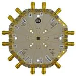
Figure 1. NB7V52MMNGEVB Evaluation
Board (Top View)
Figure 2. NB7V52MMNGEVB Evaluation
Board (Bottom View)
© Semiconductor Components Industries, LLC, 2015
July, 2015 − Rev. 0
1
Publication Order Number:
EVBUM2305/D
�NB7V52MMNGEVB
Figure 3. Enlarged Bottom View
Figure 4. Enlarged Bottom View of Evaluation Board
Figure 5. Evaluation Board Layout, 4-Layer
www.onsemi.com
2
�NB7V52MMNGEVB
Top View
Bottom View
Figure 6. Evaluation Board Layout
Evaluation Board Assembly Instructions
The power pin layout and typical connection for the
evaluation board is shown in Figure 7.
It is recommended to add bypass capacitors to reduce
unwanted noise from the power supplies. Connect 0.1 mF
capacitors from VCC and VEE/DUTGND to SMAGND.
The QFN−16 evaluation board is designed for
characterizing devices in a 50 W laboratory environment
using high bandwidth equipment. Each signal trace on the
board has a via at the DUT pin, which provides an option of
placing a termination resistor on the board bottom,
depending on the input/output configuration (See Table 1,
Example Configuration List). Table 5 contains the Bill of
Materials for this evaluation board.
The QFN16EVB was designed to accommodate a custom
QFN−16 socket. Therefore, some external components are
installed on the bottom side of the board.
Output Loading/Termination
CML Outputs
For the termination of CML outputs, operation with
negative supply voltages is recommended to enable the use
of the 50-W internal impedance of an oscilloscope or other
measurement instrument. Since CML output termination
requires 50-W to VCC, off-setting the power supply such that
VCC = 0 V and DUTGND= −2.5 V or −1.8 V, will allow
oscilloscope and VCC to be at the same potential. CML
outputs can now be conveniently terminated using the 50-W
internal impedance of oscilloscope or other measurement
instrument.
Solder the Device on the Evaluation Board
The soldering of a device to the evaluation board can be
accomplished by hand soldering or solder reflow techniques
using solder paste. Make sure pin 1 of the device is located
properly and all the pins are aligned to the footprint pads.
Solder the QFN−16 device to the evaluation board. As
mentioned earlier, many QFN16EVB’s are dedicated with
a device already installed, and can be ordered from
www.onsemi.com at the specific device webpage.
Installing SMA Connectors
Each configuration indicates the number of SMA
connectors needed to populate an evaluation board for
a given device. Each input and output requires one SMA
connector. Install all the required SMA connectors onto the
board and solder the center signal conductor pin to the board
on J1 through J16. Please note that the alignment of the
signal connector pin of the SMA connector to the metal trace
on the board can influence lab results. The launch and
reflection of the signals are largely influenced by imperfect
alignment and soldering of the SMA connector.
Connecting Power and Ground
On the top side of the evaluation board, solder the four
surface mount test pint clips (anvils) to the pads labeled
VCC, VEE/DUTGND, SMAGND, and ExPad. ExPad is
connected to the exposed flag and is typically recommended
to be tied to VEE/DUTGND, the negative supply of the
device.
The positive power supply connector is labeled VCC.
Depending on the device, the negative power supply
nomenclature is labeled either GND or VEE. To help avoid
confusion with the use of this board, the negative supply
connector is labeled VEE/DUTGND. SMAGND is the
ground for the SMA connectors and is not to be confused
with the device ground, VEE/DUTGND. SMAGND and
DUTGND can be connected in a single-supply application.
Validating the Assembled Board
After assembling the evaluation board, it is recommended
to perform continuity checks on all soldered areas before
commencing with the evaluation process. Time Domain
Reflectometry (TDR) is another highly recommended
validation test.
www.onsemi.com
3
�NB7V52MMNGEVB
Table 1. NB7V52M EVALUATION BOARD CONFIGURATION
Device
J1
J2
J3
J4
J5
J6
J7
J8
J9
J10
J11
J12
J13
J14
J15
J16
1
2
3
4
5
6
7
8
9
10
11
12
13
14
15
16
Connector
Yes
Yes
Yes
Yes
Yes
Yes
Yes
Yes
No
Yes
Yes
No
Yes
Yes
Yes
Yes
Wire
No
No
No
No
No
No
No
No
VEE
No
No
VCC
No
No
No
No
Pin #
NOTE: Exposed Pad = DUTGND, Exopsed Pad should be tied to VEE/DUTGND
Install 0.1 mF Decoupling
Capacitors
Bottom View
Install 0.1 mF Decoupling
Capacitors
Top View
Figure 7. Power Supply Configuration for NB7V52MMNGEVB
www.onsemi.com
4
�NB7V52MMNGEVB
QUICK START LAB SET-UP USER’S GUIDE
Equipment Required
1. DC Power Supply
2. Generator
3. Oscilloscope
4. DC Power Supply Connectors
5. 50-W SMA Connectors for I/O’s
Block Diagram
Figure 8. NB7V52MMNGEVB Test Block Diagram
Test and Measurement Setup Procedures
5. Connect internal 50-W pins VTCLK, VTCLK,
VTD, VTD, VTR and VTR to appropriate levels.
See Figures 9−11 for appropriate Input level
interface.
6. Connect R & R Input/Output select values to
appropriate levels. See Table 3 for levels.
1. Connect VCC, SMAGND, and VEE/DUTGND of
the NB7V52M to a DC power supply. See Table 2
for appropriate levels.
2. Connect output of generator to CLK & CLK with
50-W connectors to DUT. See NB7V52M data
sheet for appropriate input levels.
3. Connect output of generator to D & D with 50-W
connectors to DUT. See NB7V52M data sheet for
appropriate input levels.
4. Connect NB7V52M outputs Q & Q to appropriate
oscilloscope channel. Board does not have 50-W
output termination resistors, thus internal 50-W of
oscilloscope can be used to properly terminate
outputs.
NOTE:
See NB7V52M data sheet for D to CLK set up and hold
times.
Power-Up Sequence
1. Turn On DUT Power Supply
2. Enable Generator Outputs
3. Monitor Q & Q Outputs with Oscilloscope
www.onsemi.com
5
�NB7V52MMNGEVB
Table 2. POWER SUPPLY LEVELS
Outputs
Power Supply
VCC
VEE/DUTGND
SMAGND
ExPad (Typ)
CML
2.5 V
0V
−2.5 V
0V
VEE/DUTGND
CML
1.8 V
0V
−1.8 V
0V
VEE/DUTGND
Table 3. RESET INPUT/OUTPUT SELECT TRUTH TABLE
R
R
D
CLK
Q
H
L
X
X
L
L
H
L
Z
L
L
H
H
Z
H
Table 4. NB7V52M CML OUTPUTS “SPLIT” POWER SUPPLY CONFIGURATION
Device Pin Power Supply Convertor
“Split” Power Supply
VCC
VCC = 0 V
SMAGND
VTT = 0 V
DUTGND
DUTGND = −2.5 V or −1.8 V
www.onsemi.com
6
�NB7V52MMNGEVB
VCC
VCC
ZO = 50 W
NB7V52M
D, CLK, R
50 W*
VTX
LVDS
Driver
VTX
50 W*
ZO = 50 W
GND/VEE
NOTE:
D, CLK, R
VTX = VTX
GND/VEE
X = D, CLK, R & X = D, CLK, R
Figure 9. LVDS Interface
VCC
VCC
ZO = 50 W
NB7V52M
D, CLK, R
50 W*
LVPECL
Driver
VTX
VTX
50 W*
D, CLK, R
ZO = 50 W
VTX = VTX = VCC − 2 V
GND/VEE
GND/VEE
NOTE:
X = D, CLK, R & X = D, CLK, R
Figure 10. LVPECL Interface
VCC
VCC
ZO = 50 W
VCC
CML
Driver
NB7V52M
D, CLK, R
50 W*
VTX
VTX
50 W*
ZO = 50 W
D, CLK, R
VTX = VTX = VCC
GND/VEE
GND/VEE
NOTE:
X = D, CLK, R & X = D, CLK, R
Figure 11. Standard 50 W CML Interface
www.onsemi.com
7
�NB7V52MMNGEVB
SMAGND
SMAGND
SMAGND
SMAGND
SMAGND
10 mF
SMAGND
10 mF
SMAGND
13
SMAGND
VTR
14
R
15
R
VTR
SMAGND
16
VCC
0.1 mF
VTD
SMAGND
9
0.1 mF
8
6
10
VTCLK
VEE
5
SMAGND
11
SMAGND
Q
D
VTCLK
4
12
NB7V52M
CLK
SMAGND
3
Q
D
7
2
VCC
VTD
CLK
1
SMAGND
VEE/DUTGND
SMAGND
SMAGND
SMAGND
SMAGND
Figure 12. NB7V52MNGEVB Schematic
www.onsemi.com
8
�NB7V52MMNGEVB
TYPICAL OUTPUT WAVEFORMS
Figure 13. Typical Q & Q at FIN = 1 GHz, VCC = 1.8 V, 255C
Figure 14. Typical Q & Q at FIN = 10 GHz, VCC = 1.8 V, 255C
www.onsemi.com
9
�NB7V52MMNGEVB
BILL OF MATERIALS
Table 5. NB7V52MMNGEVB BILL OF MATERIALS
Components
Qty.
Description
Manufacturer
Part Number
Web Site
SMA Connector
14
SMA Connector, Side
Launch, Gold Plated
Rosenberger
32K243−40ME3
www.rosenberger.com
Surface Mount
Test Points
4
SMT Miniature Test Point
Keystone
5015
www.keyelco.com
Chip Capacitor
2
0402 0.1 mF ±10%
Kemet
C0402C105K9PACTU
www.kemet.com
Chip Capacitor
2
0603 0.1 mF ±10%
Kemet
C0603C105K8PACTU
www.kemet.com
Chip Capacitor
2
22 mF ±10%
Kemet
T495C226K025ATE300
www.kemet.com
Evaluation Board
1
QFN 16 Evaluation Board
ON Semiconductor
QFN16EVB
www.onsemi.com
Device Samples
1
QFN 16 Package Device
ON Semiconductor
NB7V52MMNG
www.onsemi.com
www.onsemi.com
10
�onsemi,
, and other names, marks, and brands are registered and/or common law trademarks of Semiconductor Components Industries, LLC dba “onsemi” or its affiliates
and/or subsidiaries in the United States and/or other countries. onsemi owns the rights to a number of patents, trademarks, copyrights, trade secrets, and other intellectual property. A
listing of onsemi’s product/patent coverage may be accessed at www.onsemi.com/site/pdf/Patent−Marking.pdf. onsemi is an Equal Opportunity/Affirmative Action Employer. This
literature is subject to all applicable copyright laws and is not for resale in any manner.
The evaluation board/kit (research and development board/kit) (hereinafter the “board”) is not a finished product and is not available for sale to consumers. The board is only intended
for research, development, demonstration and evaluation purposes and will only be used in laboratory/development areas by persons with an engineering/technical training and familiar
with the risks associated with handling electrical/mechanical components, systems and subsystems. This person assumes full responsibility/liability for proper and safe handling. Any
other use, resale or redistribution for any other purpose is strictly prohibited.
THE BOARD IS PROVIDED BY ONSEMI TO YOU “AS IS” AND WITHOUT ANY REPRESENTATIONS OR WARRANTIES WHATSOEVER. WITHOUT LIMITING THE FOREGOING,
ONSEMI (AND ITS LICENSORS/SUPPLIERS) HEREBY DISCLAIMS ANY AND ALL REPRESENTATIONS AND WARRANTIES IN RELATION TO THE BOARD, ANY
MODIFICATIONS, OR THIS AGREEMENT, WHETHER EXPRESS, IMPLIED, STATUTORY OR OTHERWISE, INCLUDING WITHOUT LIMITATION ANY AND ALL
REPRESENTATIONS AND WARRANTIES OF MERCHANTABILITY, FITNESS FOR A PARTICULAR PURPOSE, TITLE, NON−INFRINGEMENT, AND THOSE ARISING FROM A
COURSE OF DEALING, TRADE USAGE, TRADE CUSTOM OR TRADE PRACTICE.
onsemi reserves the right to make changes without further notice to any board.
You are responsible for determining whether the board will be suitable for your intended use or application or will achieve your intended results. Prior to using or distributing any systems
that have been evaluated, designed or tested using the board, you agree to test and validate your design to confirm the functionality for your application. Any technical, applications or
design information or advice, quality characterization, reliability data or other services provided by onsemi shall not constitute any representation or warranty by onsemi, and no additional
obligations or liabilities shall arise from onsemi having provided such information or services.
onsemi products including the boards are not designed, intended, or authorized for use in life support systems, or any FDA Class 3 medical devices or medical devices with a similar
or equivalent classification in a foreign jurisdiction, or any devices intended for implantation in the human body. You agree to indemnify, defend and hold harmless onsemi, its directors,
officers, employees, representatives, agents, subsidiaries, affiliates, distributors, and assigns, against any and all liabilities, losses, costs, damages, judgments, and expenses, arising
out of any claim, demand, investigation, lawsuit, regulatory action or cause of action arising out of or associated with any unauthorized use, even if such claim alleges that onsemi was
negligent regarding the design or manufacture of any products and/or the board.
This evaluation board/kit does not fall within the scope of the European Union directives regarding electromagnetic compatibility, restricted substances (RoHS), recycling (WEEE), FCC,
CE or UL, and may not meet the technical requirements of these or other related directives.
FCC WARNING – This evaluation board/kit is intended for use for engineering development, demonstration, or evaluation purposes only and is not considered by onsemi to be a finished
end product fit for general consumer use. It may generate, use, or radiate radio frequency energy and has not been tested for compliance with the limits of computing devices pursuant
to part 15 of FCC rules, which are designed to provide reasonable protection against radio frequency interference. Operation of this equipment may cause interference with radio
communications, in which case the user shall be responsible, at its expense, to take whatever measures may be required to correct this interference.
onsemi does not convey any license under its patent rights nor the rights of others.
LIMITATIONS OF LIABILITY: onsemi shall not be liable for any special, consequential, incidental, indirect or punitive damages, including, but not limited to the costs of requalification,
delay, loss of profits or goodwill, arising out of or in connection with the board, even if onsemi is advised of the possibility of such damages. In no event shall onsemi’s aggregate liability
from any obligation arising out of or in connection with the board, under any theory of liability, exceed the purchase price paid for the board, if any.
The board is provided to you subject to the license and other terms per onsemi’s standard terms and conditions of sale. For more information and documentation, please visit
www.onsemi.com.
PUBLICATION ORDERING INFORMATION
LITERATURE FULFILLMENT:
Email Requests to: orderlit@onsemi.com
onsemi Website: www.onsemi.com
◊
TECHNICAL SUPPORT
North American Technical Support:
Voice Mail: 1 800−282−9855 Toll Free USA/Canada
Phone: 011 421 33 790 2910
www.onsemi.com
1
Europe, Middle East and Africa Technical Support:
Phone: 00421 33 790 2910
For additional information, please contact your local Sales Representative
�


 工商网监
湘ICP备2023018690号
工商网监
湘ICP备2023018690号
