NB7L1008MNGEVB
NB7L1008MNG Evaluation
Board User's Manual
Introduction
The NB7L1008 is a high performance differential
1:8 Clock/Data fanout buffer that operates up to
12 Gbps/7 GHz with a 2.5 V or 3.3 V power supply.
ON Semiconductor has developed a “universal” QFN−32
evaluation board and configured it for the NB7L1008. This
evaluation board was designed to provide a flexible and
convenient platform to quickly evaluate, characterize and
verify the operation of the NB7L1008.
This evaluation board manual contains:
• Information on the NB7L1008 Evaluation Board
• Test and Measurement Setup Procedures
www.onsemi.com
EVAL BOARD USER’S MANUAL
Layer Stack
L1 (Rogers)
High-performance SMA connectors are provided for all
high-speed input & output signal access.
This manual should be used in conjunction with the device
datasheet, which contains full technical details on the device
specifications and operation.
Evaluation Board Assembly Instructions
The QFN−32 evaluation board is designed for
characterizing devices in a 50-W laboratory environment
using high bandwidth equipment.
Board Layout
The NB7L1008 Evaluation Board provides a high
bandwidth, 50-W controlled impedance environment and is
implemented in one layer.
Output Loading/Termination
LVPECL Outputs
Table 1. DIFFERENTIAL INPUTS DRIVEN SINGLE – ENDED (Notes 1 & 2)
Symbol
Min
Typ
Max
Unit
VIH
Single – Ended Input High Voltage
Vth + 75
−
VCC
mV
VIL
Single – Ended Input Low Voltage
VEE
−
Vth − 100
mV
Vth
Input Threshold Reference Voltage Range
VEE + 1100
−
VCC − 100
mV
200
−
1200
mV
Min
Typ
Max
Unit
VISE
Characteristic
Single – Ended Input Voltage (VIH – VIL)
1. Vth, VIH, VIL and VISE parameters must be complied with simultaneously.
2. Vth is applied to the complementary input when operating in single-ended mode.
Table 2. DIFFERENTIAL INPUTS DRIVEN DIFFERENTIALLY (IN, INB) (Note 3)
Symbol
Characteristic
VIHD
Differential Input High Voltage
VEE + 1100
−
VCC
mV
VILD
Differential Input Low Voltage
VEE
−
VIHD − 100
mV
VID
Differential Input Voltage (VIHD – VILD)
100
−
1200
mV
IIH
Input High Current
−150
40
+150
mA
IIL
Input Low Current
−150
5
+150
mA
3. VIHD, VILD, VID and VCMR parameters must be complied with simultaneously.
If the input signals to the NB7L1008 require termination,
internal 50-W resistors are provided via the VT pin and
grounded using a SMA grounding plug then and should be
stimulated with the appropriate voltage levels.
© Semiconductor Components Industries, LLC, 2014
July, 2017 − Rev. 2
NOTE: For this evaluation board, VT is connected to
ground, thus it can only be used for LVPECL
inputs.
1
Publication Order Number:
EVBUM2241/D
�NB7L1008MNGEVB
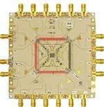
Figure 1. Test Board
1. Connect the appropriate power supplies to VCC,
DUTGND.
2. Connect a signal generator to the input SMA
connectors. Setup input signal levels according to
the device data sheet.
3. Connect a test measurement device to the device’s
output SMA connectors.
NOTE: The test measurement device must contain 50-W
termination.
Table 3. NB7L1008, LVPECL INPUTS AND LVPECL OUTPUTS
Device Pin Power Supply Connector
Power Supply
VCC
VCC = 2 V
50 W Input
VT = 0 V
DUTGND
DUTGND = VEE = −0.5 V (for 2.5 V) and −1.3 V (for 3.3 V)
Table 4. NB7L1008, CML INPUTS AND LVPECL OUTPUTS
Device Pin Power Supply Connector
Power Supply
VCC
VCC = 2 V
50 W Input
VT = VCC
DUTGND
DUTGND = VEE = −0.5 V (for 2.5 V) and −1.3 V (for 3.3 V)
Table 5. NB7L1008, LVDS INPUTS AND LVPECL OUTPUTS
Device Pin Power Supply Connector
Power Supply
VCC
VCC = 2 V
50 W Input
VT = Open
DUTGND
DUTGND = VEE = −0.5 V (for 2.5 V) and −1.3 V (for 3.3 V)
www.onsemi.com
2
�NB7L1008MNGEVB
Figure 2. Schematic Drawing
Table 6. BILL OF MATERIALS
Manufacturer
Part Number
Components
Manufacturer
Description
SMA Connector
Rosenberger
High Performance
SMA Connector, Side
Launch, Gold Plated
32K243-40ME3
http://www.rosenberger.de
http://www.rosenbergerna.com
SMA Connector
Johnson-Emerson
SMA Connector, Side
Launch, Gold Plated
142-0701-801
http://www.digikey.com
Surface Mount Test
Points
Keystone*
SMT Compact Test
Point
5016
http://www.keylco.com
Chip Capacitor
AVC Corporation*
0603 0.1 mF ±10%
0603C104KAT2A
http://www.avxcorp.com
Chip Capacitor
Kemet
1206 0.01 mF ±10%
C1206C103K5RACTU
http://www.newark.com
Chip Capacitor
TDK
0603 0.1 mF ±10%
C3216X5R1H106K160AB
http://www.newark.com
Evaluation Board
ON Semiconductor
QFN 32 Evaluation
Board − 2−Layer
http://www.onsemi.com
Device Samples
ON Semiconductor
NB7L1008MNG
http://www.onsemi.com
*Components are available through most distributors, i.e. www.newark.com, www.Digikey.com
www.onsemi.com
3
Web Site
�onsemi,
, and other names, marks, and brands are registered and/or common law trademarks of Semiconductor Components Industries, LLC dba “onsemi” or its affiliates
and/or subsidiaries in the United States and/or other countries. onsemi owns the rights to a number of patents, trademarks, copyrights, trade secrets, and other intellectual property. A
listing of onsemi’s product/patent coverage may be accessed at www.onsemi.com/site/pdf/Patent−Marking.pdf. onsemi is an Equal Opportunity/Affirmative Action Employer. This
literature is subject to all applicable copyright laws and is not for resale in any manner.
The evaluation board/kit (research and development board/kit) (hereinafter the “board”) is not a finished product and is not available for sale to consumers. The board is only intended
for research, development, demonstration and evaluation purposes and will only be used in laboratory/development areas by persons with an engineering/technical training and familiar
with the risks associated with handling electrical/mechanical components, systems and subsystems. This person assumes full responsibility/liability for proper and safe handling. Any
other use, resale or redistribution for any other purpose is strictly prohibited.
THE BOARD IS PROVIDED BY ONSEMI TO YOU “AS IS” AND WITHOUT ANY REPRESENTATIONS OR WARRANTIES WHATSOEVER. WITHOUT LIMITING THE FOREGOING,
ONSEMI (AND ITS LICENSORS/SUPPLIERS) HEREBY DISCLAIMS ANY AND ALL REPRESENTATIONS AND WARRANTIES IN RELATION TO THE BOARD, ANY
MODIFICATIONS, OR THIS AGREEMENT, WHETHER EXPRESS, IMPLIED, STATUTORY OR OTHERWISE, INCLUDING WITHOUT LIMITATION ANY AND ALL
REPRESENTATIONS AND WARRANTIES OF MERCHANTABILITY, FITNESS FOR A PARTICULAR PURPOSE, TITLE, NON−INFRINGEMENT, AND THOSE ARISING FROM A
COURSE OF DEALING, TRADE USAGE, TRADE CUSTOM OR TRADE PRACTICE.
onsemi reserves the right to make changes without further notice to any board.
You are responsible for determining whether the board will be suitable for your intended use or application or will achieve your intended results. Prior to using or distributing any systems
that have been evaluated, designed or tested using the board, you agree to test and validate your design to confirm the functionality for your application. Any technical, applications or
design information or advice, quality characterization, reliability data or other services provided by onsemi shall not constitute any representation or warranty by onsemi, and no additional
obligations or liabilities shall arise from onsemi having provided such information or services.
onsemi products including the boards are not designed, intended, or authorized for use in life support systems, or any FDA Class 3 medical devices or medical devices with a similar
or equivalent classification in a foreign jurisdiction, or any devices intended for implantation in the human body. You agree to indemnify, defend and hold harmless onsemi, its directors,
officers, employees, representatives, agents, subsidiaries, affiliates, distributors, and assigns, against any and all liabilities, losses, costs, damages, judgments, and expenses, arising
out of any claim, demand, investigation, lawsuit, regulatory action or cause of action arising out of or associated with any unauthorized use, even if such claim alleges that onsemi was
negligent regarding the design or manufacture of any products and/or the board.
This evaluation board/kit does not fall within the scope of the European Union directives regarding electromagnetic compatibility, restricted substances (RoHS), recycling (WEEE), FCC,
CE or UL, and may not meet the technical requirements of these or other related directives.
FCC WARNING – This evaluation board/kit is intended for use for engineering development, demonstration, or evaluation purposes only and is not considered by onsemi to be a finished
end product fit for general consumer use. It may generate, use, or radiate radio frequency energy and has not been tested for compliance with the limits of computing devices pursuant
to part 15 of FCC rules, which are designed to provide reasonable protection against radio frequency interference. Operation of this equipment may cause interference with radio
communications, in which case the user shall be responsible, at its expense, to take whatever measures may be required to correct this interference.
onsemi does not convey any license under its patent rights nor the rights of others.
LIMITATIONS OF LIABILITY: onsemi shall not be liable for any special, consequential, incidental, indirect or punitive damages, including, but not limited to the costs of requalification,
delay, loss of profits or goodwill, arising out of or in connection with the board, even if onsemi is advised of the possibility of such damages. In no event shall onsemi’s aggregate liability
from any obligation arising out of or in connection with the board, under any theory of liability, exceed the purchase price paid for the board, if any.
The board is provided to you subject to the license and other terms per onsemi’s standard terms and conditions of sale. For more information and documentation, please visit
www.onsemi.com.
PUBLICATION ORDERING INFORMATION
LITERATURE FULFILLMENT:
Email Requests to: orderlit@onsemi.com
onsemi Website: www.onsemi.com
◊
TECHNICAL SUPPORT
North American Technical Support:
Voice Mail: 1 800−282−9855 Toll Free USA/Canada
Phone: 011 421 33 790 2910
www.onsemi.com
1
Europe, Middle East and Africa Technical Support:
Phone: 00421 33 790 2910
For additional information, please contact your local Sales Representative
�


 工商网监
湘ICP备2023018690号
工商网监
湘ICP备2023018690号
