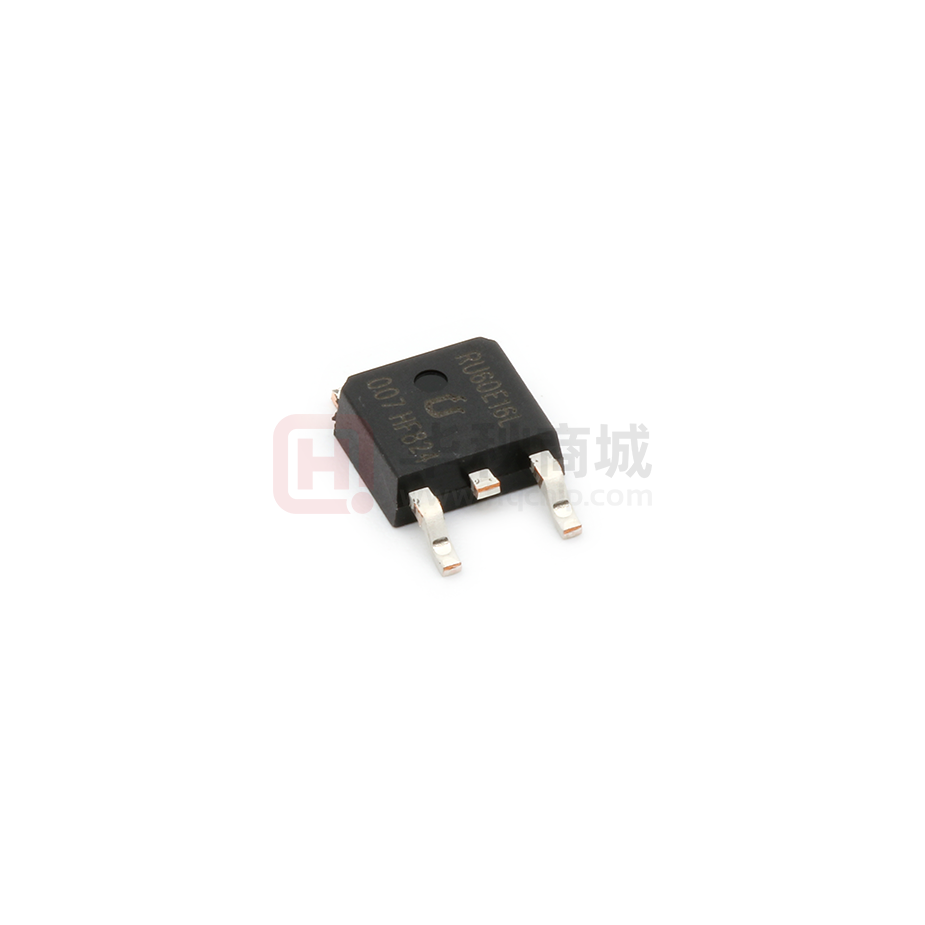
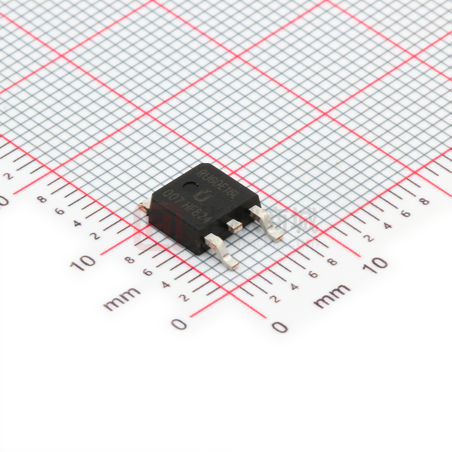
RU60E16L
N-Channel Advanced Power MOSFET
MOSFET
Features
Pin Description
• 60V/16A,
RDS (ON) =60mΩ(Typ.)@VGS=10V
RDS (ON) =75mΩ(Typ.)@VGS=4.5V
• Super High Dense Cell Design
• ESD protected
• Reliable and Rugged
TO252
• 100% avalanche tested
• Lead Free and Green Devices Available
(RoHS Compliant)
Applications
• Power Management
N-Channel MOSFET
Absolute Maximum Ratings
Symbol
Parameter
Rating
Unit
Common Ratings (TC=25°C Unless Otherwise Noted)
VDSS
Drain-Source Voltage
60
VGSS
Gate-Source Voltage
±20
Maximum Junction Temperature
175
°C
-55 to 175
°C
16
A
TJ
TSTG
IS
Storage Temperature Range
Diode Continuous Forward Current
TC=25°C
V
Mounted on Large Heat Sink
IDP
300μs Pulse Drain Current Tested
ID
Continuous Drain Current(VGS=10V)
PD
RθJC
Maximum Power Dissipation
Thermal Resistance-Junction to Case
①
TC=25°C
64
TC=25°C
TC=100°C
16
11.5
TC=25°C
40
TC=100°C
20
A
②
A
W
3.75
°C/W
25
mJ
Drain-Source Avalanche Ratings
EAS
③
Avalanche Energy, Single Pulsed
Copyright Ruichips Semiconductor Co., Ltd
Rev. C– JUN., 2011
www.ruichips.com
�RU60E16L
Electrical Characteristics
Symbol
(TC=25°C Unless Otherwise Noted)
Parameter
Static Characteristics
BVDSS Drain-Source Breakdown Voltage
IDSS
Zero Gate Voltage Drain Current
VGS(th)
IGSS
RDS(ON)
④
Test Condition
VGS=0V, IDS=250µA
RU60E16L
Min.
Typ.
1
TJ=85°C
VDS=VGS, IDS=250µA
Gate Leakage Current
VGS=±16V, VDS=0V
Unit
V
60
VDS= 60V, VGS=0V
Gate Threshold Voltage
Max.
30
1.5
2
µA
2.7
V
±10
µA
VGS= 10V, IDS=8A
60
75
mΩ
VGS= 4.5V, IDS=5.5A
75
90
mΩ
1.2
V
Drain-Source On-state Resistance
Diode Characteristics
VSD
④
Diode Forward Voltage
trr
Reverse Recovery Time
Qrr
Reverse Recovery Charge
ISD=8A, VGS=0V
38
ns
67
nC
VGS=0V,VDS=0V,F=1MHz
1.3
Ω
VGS=0V,
VDS= 30V,
Frequency=1.0MHz
480
ISD=8A, dlSD/dt=100A/µs
⑤
Dynamic Characteristics
RG
Gate Resistance
Ciss
Input Capacitance
Coss
Output Capacitance
Crss
Reverse Transfer Capacitance
td(ON)
Turn-on Delay Time
tr
Turn-on Rise Time
td(OFF)
Turn-off Delay Time
tf
pF
75
48
15
VDD=30V, RL=3.8Ω,
IDS=8A, VGEN= 10V,
RG=4.7Ω
Turn-off Fall Time
18
ns
33
16
⑤
Gate Charge Characteristics
Qg
Total Gate Charge
Qgs
Gate-Source Charge
Qgd
Gate-Drain Charge
Notes:
14
VDS=48V, VGS= 10V,
IDS=8A
2.9
18
nC
5.2
Pulse width limited by safe operating area.
Calculated continuous current based on maximum allowable junction temperature.
Limited by TJmax, IAS =10A, VDD = 48V, RG = 50Ω , Starting TJ = 25°C.
Pulse test ; Pulse width≤300µs, duty cycle≤2%.
Guaranteed by design, not subject to production testing.
Copyright Ruichips Semiconductor Co., Ltd
Rev. C– JUN., 2011
2
www.ruichips.com
�RU60E16L
Typical Characteristics
Drain Current
Ptot - Power (W)
ID - Drain Current (A)
Power Dissipation
Tj - Junction Temperature (°C)
Tj - Junction Temperature (°C)
Safe Operation Area
ID - Drain Current (A)
Normalized Effective Transient
Thermal Transient Impedance
VDS - Drain-Source Voltage (V)
Copyright Ruichips Semiconductor Co., Ltd
Rev. C– JUN., 2011
Square Wave Pulse Duration (sec)
3
www.ruichips.com
�RU60E16L
Typical Characteristics
Drain-Source On Resistance
ID - Drain Current (A)
RDS(ON) - On Resistance (mΩ)
Output Characteristics
VDS - Drain-Source Voltage (V)
ID - Drain Current (A)
Gate Threshold Voltage
RDS(ON) - On - Resistance (m)
Normalized Threshold Voltage
Drain-Source On Resistance
VGS - Gate-Source Voltage (V)
Copyright Ruichips Semiconductor Co., Ltd
Rev. C– JUN., 2011
Tj - Junction Temperature (°C)
4
www.ruichips.com
�RU60E16L
Typical Characteristics
Source-Drain Diode Forward
IS - Source Current (A)
Normalized On Resistance
Drain-Source On Resistance
Tj - Junction Temperature (°C)
VSD - Source-Drain Voltage (V)
Gate Charge
C - Capacitance (pF)
VGS - Gate-Source Voltage (V)
Capacitance
VDS - Drain-Source Voltage (V)
Copyright Ruichips Semiconductor Co., Ltd
Rev. C– JUN., 2011
QG - Gate Charge (nC)
5
www.ruichips.com
�RU60E16L
Avalanche Test Circuit and Waveforms
Switching Time Test Circuit and Waveforms
Copyright Ruichips Semiconductor Co., Ltd
Rev. C– JUN., 2011
6
www.ruichips.com
�RU60E16L
Ordering and Marking Information
Device
Marking
Package
Packaging
Quantity
Reel Size
Tape width
RU60E16L
RU60E16L
TO-252
Tape&Reel
2500
13’’
16mm
Copyright Ruichips Semiconductor Co., Ltd
Rev. C– JUN., 2011
7
www.ruichips.com
�RU60E16L
Package Information
TO252-2L
SYMBOL
MM
INCH
MM
SYMBOL
MIN
MAX
MIN
MAX
A
2.200
2.400
0.087
0.094
L
A1
0.000
0.127
0.000
0.005
L1
INCH
MIN
MAX
MIN
MAX
9.800
10.400
0.386
0.409
2.900 REF.
b
0.660
0.860
0.026
0.034
L2
C
0.460
0.580
0.018
0.023
L3
D
6.500
6.700
0.256
0.264
L4
0.600
1.000
0.024
0.039
D1
5.100
5.460
0.201
0.215
Φ
1.100
1.300
0.043
0.051
θ
0°
8°
0°
8°
0.000
0.300
0.000
0.012
D2
4.830 REF.
0.190 REF.
E
6.000
6.200
0.236
0.244
h
e
2.186
2.386
0.086
0.094
V
1.400
1.700
0.114 REF.
1.600 REF.
5.350 REF.
0.055
0.067
0.063REF.
0.211 REF.
ALL DIMENSIONS REFER TO JEDEC STANDARD
DO NOT INCLUDE MOLD FLASH OR PROTRUSIONS
Copyright Ruichips Semiconductor Co., Ltd
Rev. C– JUN., 2011
8
www.ruichips.com
�RU60E16L
Customer Service
Worldwide Sales and Service:
Sales@ruichips.com
Technical Support:
Technical@ruichips.com
Investor Relations Contacts:
Investor@ruichips.com
Marcom Contact:
Marcom@ruichips.com
Editorial Contact:
Editorial@ruichips.com
HR Contact:
HR@ruichips.com
Legal Contact:
Legal@ruichips.com
Shen Zhen RUICHIPS Semiconductor CO., LTD
Room 501, the 5floor An Tong Industrial Building,
NO.207 Mei Hua Road Fu Tian Area Shen Zhen City, CHINA
TEL: (86-755) 8311-5334
FAX: (86-755) 8311-4278
E-mail: Sales-SZ@ruichips.com
Copyright Ruichips Semiconductor Co., Ltd
Rev. C– JUN., 2011
9
www.ruichips.com
�


 工商网监
湘ICP备2023018690号
工商网监
湘ICP备2023018690号
