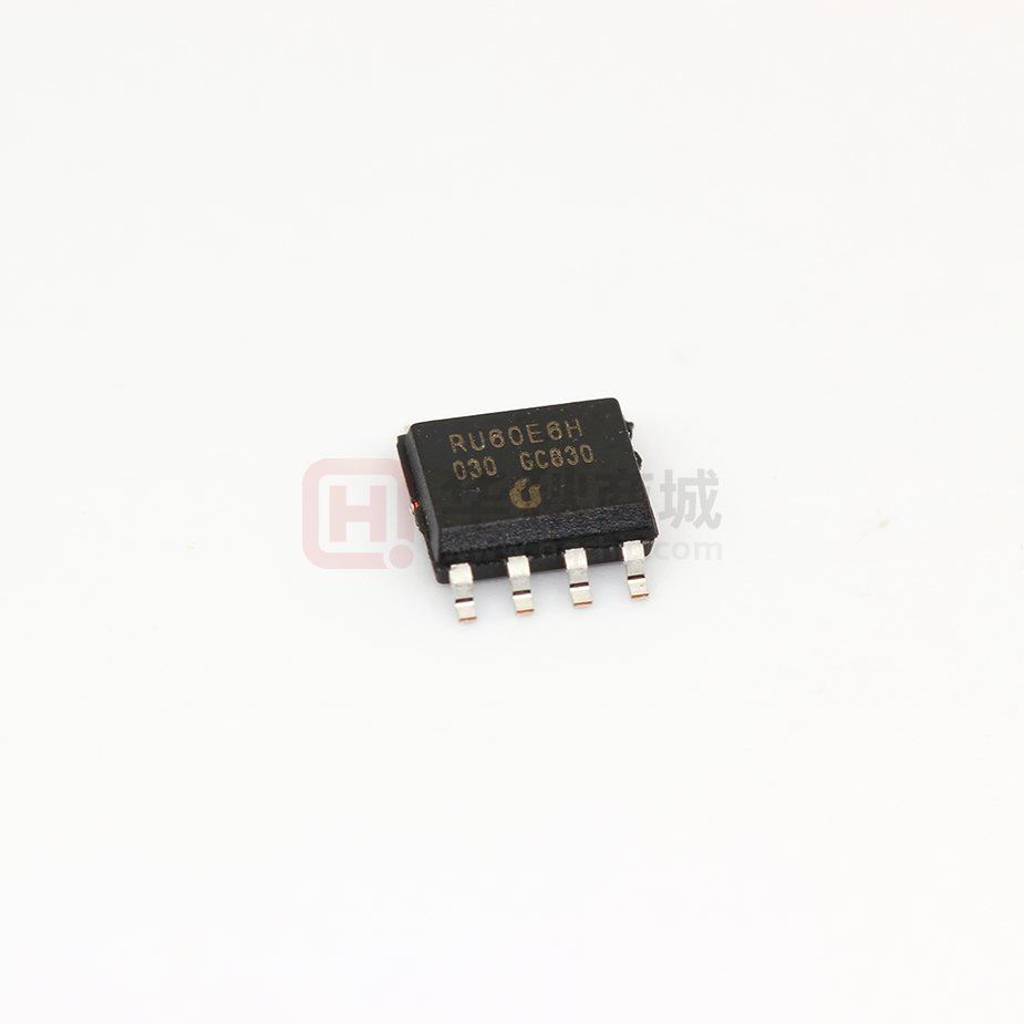
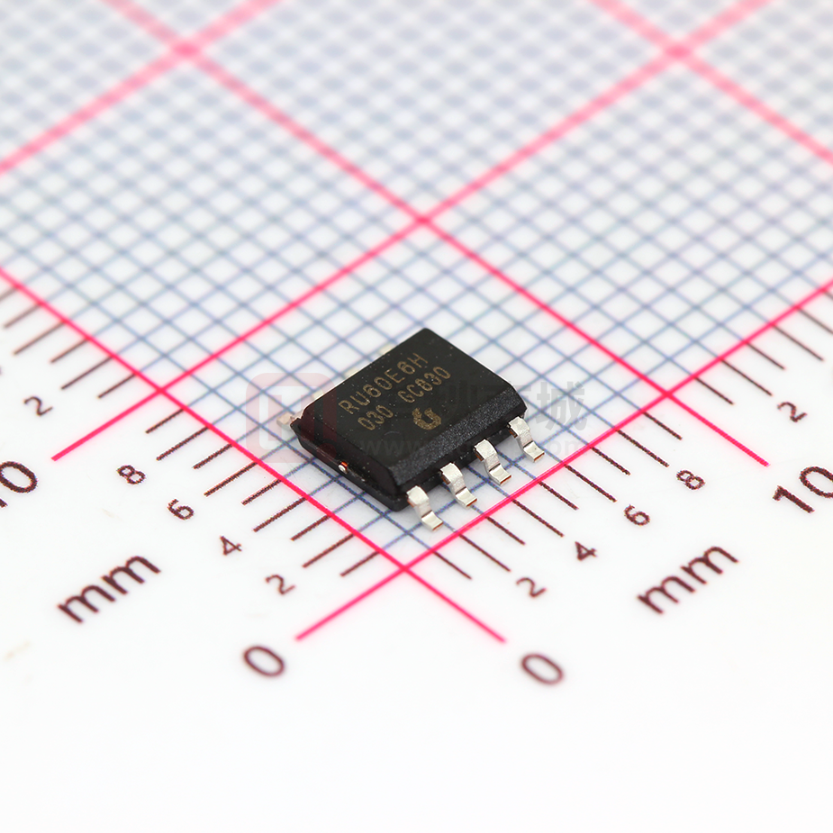
RU60E6H
N-Channel Advanced Power MOSFET
MOSFET
Features
Pin Description
• 60V/6A,
RDS (ON) =31mΩ (Type) @ VGS=10V
RDS (ON) =37mΩ (Type) @ VGS=4.5V
• Super High Dense Cell Design
• Reliable and Rugged
• ESD Protected
SOP-8
• Lead Free and Green Available
Applications
• Power Management.
• Switch Applications.
Absolute Maximum Ratings
Symbol
N-Channel MOSFET
Parameter
Rating
Unit
Common Ratings (TA=25°C Unless Otherwise Noted)
VDSS
Drain-Source Voltage
60
VGSS
Gate-Source Voltage
±20
Maximum Junction Temperature
150
°C
-55 to 150
°C
TC=25°C
6
A
TC=25°C
24
TC=25°C
6
TC=70°C
4.6
TC=25°C
2.5
TC=70°C
1.6
TJ
TSTG
IS
Storage Temperature Range
Diode Continuous Forward Current
V
Mounted on Large Heat Sink
IDP
300μs Pulse Drain Current Tested
ID
Continuous Drain Current(VGS=10V)
PD
RθJA
②
Maximum Power Dissipation
Thermal Resistance-Junction to Ambient
Copyright Ruichips Semiconductor Co., Ltd
Rev. B– APR., 2011
①
50
A
A
W
°C/W
www.ruichips.com
�RU60E6H
Electrical Characteristics
Symbol
(TA=25°C Unless Otherwise Noted)
Parameter
Static Characteristics
BVDSS Drain-Source Breakdown Voltage
IDSS
VGS(th)
IGSS
RDS(ON)
③
Zero Gate Voltage Drain Current
Test Condition
VGS=0V, IDS=250µA
RU60E6H
Min.
Typ.
1
TJ=85°C
VDS=VGS, IDS=250µA
Gate Leakage Current
VGS=±20V, VDS=0V
30
1.5
Unit
V
60
VDS= 60V, VGS=0V
Gate Threshold Voltage
Max.
2
µA
2.7
V
±10
µA
VGS= 10V, IDS=6A
31
35
mΩ
VGS= 4.5V, IDS=4A
37
45
mΩ
1.2
V
Drain-Source On-state Resistance
Diode Characteristics
VSD
③
Diode Forward Voltage
trr
Reverse Recovery Time
Qrr
Reverse Recovery Charge
ISD=6A, VGS=0V
ISD=6A, dlSD/dt=100A/µs
42
ns
73
nC
1.2
Ω
④
Dynamic Characteristics
RG
Gate Resistance
VGS=0V,VDS=0V,F=1MHz
Ciss
Input Capacitance
Coss
Output Capacitance
Crss
Reverse Transfer Capacitance
td(ON)
Turn-on Delay Time
tr
Turn-on Rise Time
td(OFF)
Turn-off Delay Time
tf
VGS=0V,
VDS= 30V,
Frequency=1.0MHz
1620
300
pF
105
12
VDD=30V, RL=30Ω,
IDS=6A, VGEN= 10V,
RG=6Ω
Turn-off Fall Time
39
34
ns
13
④
Gate Charge Characteristics
Qg
Total Gate Charge
Qgs
Gate-Source Charge
Qgd
Gate-Drain Charge
Notes:
19
VDS=48V, VGS= 10V,
IDS=6A
4
nC
9
Pulse width limited by safe operating area.
②When mounted on 1 inch square copper board, t ≤10sec.
Pulse test ; Pulse width≤300µs, duty cycle≤2%.
Guaranteed by design, not subject to production testing.
Copyright Ruichips Semiconductor Co., Ltd
Rev. B– APR., 2011
2
www.ruichips.com
�RU60E6H
Typical Characteristics
Drain Current
Ptot - Power (W)
ID - Drain Current (A)
Power Dissipation
Tj - Junction Temperature (°C)
Tj - Junction Temperature (°C)
Safe Operation Area
ID - Drain Current (A)
Normalized Effective Transient
Thermal Transient Impedance
VDS - Drain-Source Voltage (V)
Copyright Ruichips Semiconductor Co., Ltd
Rev. B– APR., 2011
Square Wave Pulse Duration (sec)
3
www.ruichips.com
�RU60E6H
Typical Characteristics
Drain-Source On Resistance
ID - Drain Current (A)
RDS(ON) - On Resistance (mΩ)
Output Characteristics
VDS - Drain-Source Voltage (V)
ID - Drain Current (A)
Gate Threshold Voltage
RDS(ON) - On - Resistance (m)
Normalized Threshold Voltage
Drain-Source On Resistance
VGS - Gate-Source Voltage (V)
Copyright Ruichips Semiconductor Co., Ltd
Rev. B– APR., 2011
Tj - Junction Temperature (°C)
4
www.ruichips.com
�RU60E6H
Typical Characteristics
Source-Drain Diode Forward
IS - Source Current (A)
Normalized On Resistance
Drain-Source On Resistance
Tj - Junction Temperature (°C)
VSD - Source-Drain Voltage (V)
Gate Charge
C - Capacitance (pF)
VGS - Gate-Source Voltage (V)
Capacitance
VDS - Drain-Source Voltage (V)
Copyright Ruichips Semiconductor Co., Ltd
Rev. B– APR., 2011
QG - Gate Charge (nC)
5
www.ruichips.com
�RU60E6H
Avalanche Test Circuit and Waveforms
Switching Time Test Circuit and Waveforms
Copyright Ruichips Semiconductor Co., Ltd
Rev. B– APR., 2011
6
www.ruichips.com
�RU60E6H
Ordering and Marking Information
Device
Marking
Package
Packaging
Quantity
Reel Size
Tape width
RU60E6H
RU60E6H
SOP-8
Tape&Reel
2500
13’’
12mm
Copyright Ruichips Semiconductor Co., Ltd
Rev. B– APR., 2011
7
www.ruichips.com
�RU60E6H
Package Information
SOP-8
SYMBOL
MM
INCH
MIN
MAX
MIN
MAX
MM
SYMBOL
INCH
MIN
MAX
MIN
MAX
A
1.350
1.750
0.053
0.069
E
3.800
4.000
0.150
0.157
A1
0.100
0.250
0.004
0.010
E1
5.800
6.200
0.228
0.244
A2
1.350
1.550
0.053
0.061
e
b
0.330
0.510
0.013
0.020
L
0.400
1.270
0.016
0.050
c
0.170
0.250
0.006
0.010
θ
0°
8°
0°
8°
D
4.700
5.100
0.185
0.200
1.270 (BSC)
0.050 (BSC)
ALL DIMENSIONS REFER TO JEDEC STANDARD
DO NOT INCLUDE MOLD FLASH OR PROTRUSIONS
Copyright Ruichips Semiconductor Co., Ltd
Rev. B– APR., 2011
8
www.ruichips.com
�RU60E6H
Customer Service
Worldwide Sales and Service:
Sales@ruichips.com
Technical Support:
Technical@ruichips.com
Investor Relations Contacts:
Investor@ruichips.com
Marcom Contact:
Marcom@ruichips.com
Editorial Contact:
Editorial@ruichips.com
HR Contact:
HR@ruichips.com
Legal Contact:
Legal@ruichips.com
Shen Zhen RUICHIPS Semiconductor CO., LTD
Room 501, the 5floor An Tong Industrial Building,
NO.207 Mei Hua Road Fu Tian Area Shen Zhen City, CHINA
TEL: (86-755) 8311-5334
FAX: (86-755) 8311-4278
E-mail: Sales-SZ@ruichips.com
Copyright Ruichips Semiconductor Co., Ltd
Rev. B– APR., 2011
9
www.ruichips.com
�
很抱歉,暂时无法提供与“RU60E6H”相匹配的价格&库存,您可以联系我们找货
免费人工找货- 国内价格
- 1+0.67500
- 100+0.63000
- 300+0.58500
- 500+0.54000
- 2000+0.51750
- 5000+0.50400


 工商网监
湘ICP备2023018690号
工商网监
湘ICP备2023018690号
