STG5683
Low voltage dual SPDTswitch
with negative rail capability
Features
■
Distortion-free negative signal throughput
down to VCC-5.5V
■
Wide operating voltage range:
VCC (Opr) = 1.65V to 4.5V single supply
■
Ultra low power dissipation:
ICC = 0.2µA (Max.) at tA = 85°C
)
s
(
ct
u
d
o
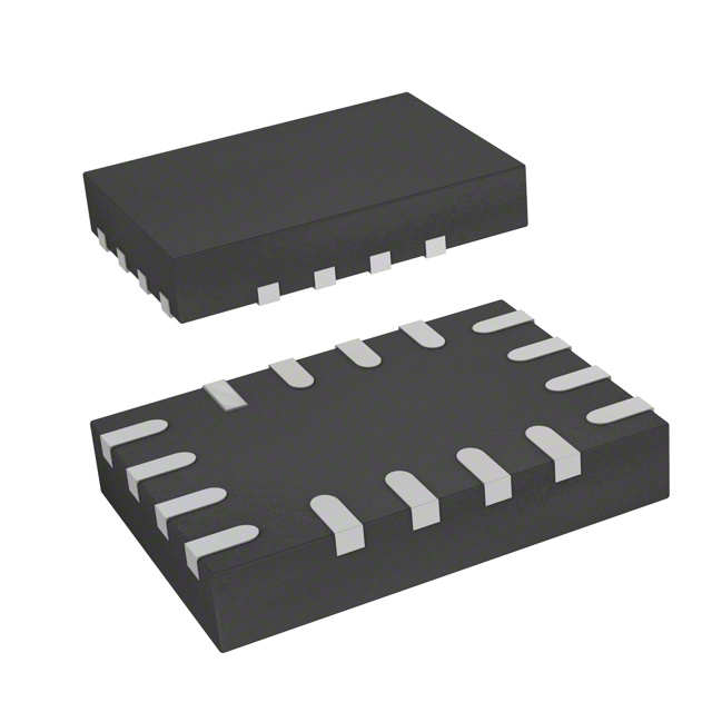
QFN16L (2.6mm x 1.8mm)
■
Low "ON" resistance VIN = 0V:
RON = 0.5Ω (max. tA = 25°C) at VCC = 4.3V
■
4.3V tolerant and 1.8V compatible threshold on
digital control input at VCC = 1.65 to 3.0V
■
Latch-up performance exceeds 300mA
(JESD 17)
■
ESD performance exceeds JESD22
■
2000-V human-body model (A114-A)
r
P
e
t
e
l
o
)
(s
Description
s
b
O
t
c
u
The STG5683 is a high-speed CMOS low voltage
dual analog S.P.D.T. (Single Pole Dual Throw)
SWITCH or 2:1 Multiplexer /Demultiplexer Switch
fabricated in silicon gate C2MOS technology. It is
designed to operate from 1.65V to 4.5V, making
this device ideal for portable applications.
d
o
r
P
e
t
e
l
o
Additional key features are fast switching speed,
Break Before Make Delay Time and Ultra Low
Power Consumption. All inputs and outputs are
equipped with protection circuits against static
discharge, giving them ESD immunity and
transient excess voltage.
s
b
O
Figure 1.
July 2007
Device summary
Order code
Package
Packaging
STG5683QTR
QFN16L (2.6mm x 1.8mm)
Tape and reel
Rev 3
1/16
www.st.com
16
�Contents
STG5683
Contents
1
Pin settings . . . . . . . . . . . . . . . . . . . . . . . . . . . . . . . . . . . . . . . . . . . . . . . . 3
1.1
Pin connection . . . . . . . . . . . . . . . . . . . . . . . . . . . . . . . . . . . . . . . . . . . . . . 3
1.2
Pin description . . . . . . . . . . . . . . . . . . . . . . . . . . . . . . . . . . . . . . . . . . . . . . 3
2
Device summary . . . . . . . . . . . . . . . . . . . . . . . . . . . . . . . . . . . . . . . . . . . . 4
3
Maximum rating . . . . . . . . . . . . . . . . . . . . . . . . . . . . . . . . . . . . . . . . . . . . . 5
3.1
)
s
(
ct
Recommended operating conditions . . . . . . . . . . . . . . . . . . . . . . . . . . . . . 6
u
d
o
4
Electrical characteristics . . . . . . . . . . . . . . . . . . . . . . . . . . . . . . . . . . . . . 7
5
Package mechanical data . . . . . . . . . . . . . . . . . . . . . . . . . . . . . . . . . . . . 11
6
Revision history . . . . . . . . . . . . . . . . . . . . . . . . . . . . . . . . . . . . . . . . . . . 15
r
P
e
t
e
l
o
)
(s
t
c
u
d
o
r
P
e
t
e
l
o
s
b
O
2/16
s
b
O
�STG5683
Pin settings
1
Pin settings
1.1
Pin connection
Figure 2.
Pin connection (top through view)
NC
15
14
13
NC
16
NC
NC
)
s
(
ct
Shunt switch
1
1SEL
12
u
d
o
2
1S2
e
t
e
l
3
D1
D2
10
2S1
9
2SEL
GND
VCC
r
P
e
11
8
7
NC
NC
u
d
o
5
s
(
t
c
6
O
)
Shunt switch
Pr
o
s
b
4
1S1
2S2
Pin
t description
e
l
o
1.2
s
b
O
Table 1. Pin description
Pin N°
Symbol
Name and function
4, 2,
10, 12
1S1, 1S2,
2S1, 2S2
3, 11
D1, D2
1, 9
1SEL, 2SEL
7
VCC
Positive supply voltage
8
GND
Ground (0V)
5,6,13,14,15,16
NC
No connect
Independent channels
Common channel
Control
3/16
�Device summary
2
STG5683
Device summary
Figure 3.
Input equivalent circuit
S2
D
)
s
(
ct
u
d
o
S1
r
P
e
t
e
l
o
SEL
)
(s
Table 2. Truth table
SEL
t
c
u
H
od
L
r
P
e
1. Shorted to ground by the shunt switch
t
e
l
o
s
b
O
4/16
s
b
O
Switch S1
Switch S2
ON
OFF (1)
OFF (1)
ON
�STG5683
3
Maximum rating
Maximum rating
Stressing the device above the rating listed in the “Absolute Maximum Ratings” table may
cause permanent damage to the device. These are stress ratings only and operation of the
device at these or any other conditions above those indicated in the Operating sections of
this specification is not implied. Exposure to Absolute Maximum Rating conditions for
extended periods may affect device reliability. Refer also to the STMicroelectronics SURE
Program and other relevant quality documents.
Table 3. Absolute maximum ratings
Symbol
VCC
Parameter
Supply voltage
DC input voltage
VIC
DC control input voltage
VO
DC output voltage
IIKC
DC input diode current on control pin (VSEL
很抱歉,暂时无法提供与“STG5683QTR”相匹配的价格&库存,您可以联系我们找货
免费人工找货- 国内价格 香港价格
- 3000+10.870993000+1.31587
- 6000+10.468356000+1.26713


 工商网监
湘ICP备2023018690号
工商网监
湘ICP备2023018690号
