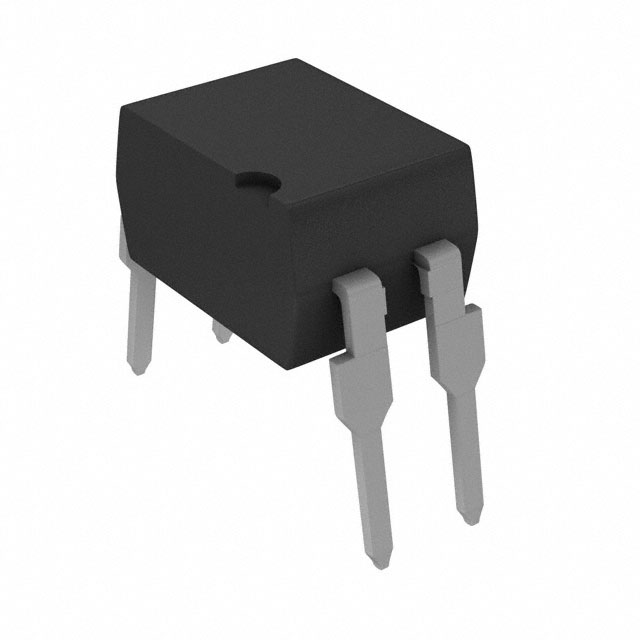
K814P, K824P, K844P
Vishay Semiconductors
Optocoupler, Phototransistor Output, AC Input
FEATURES
• Endstackable to 2.54 mm (0.1") spacing
• DC isolation test voltage VISO = 5000 VRMS
• Low coupling capacitance of typical 0.3 pF
• Current transfer ratio (CTR) of typical 100 %
• Low temperature coefficient of CTR
• Wide ambient temperature range
C
• Lead (Pb)-free component
E
• Component in accordance to RoHS 2002/95/EC and
WEEE 2002/96/EC
APPLICATIONS
• Feature phones
1
A
4 pin
• Answering machines
C
8 pin
• PBX
16 pin
• Fax machines
17220_2
AGENCY APPROVALS
C
DESCRIPTION
• UL1577, file no. E76222 system code U, double protection
The K814P, K824P, K844P consist of a phototransistor
optically coupled to 2 gallium arsenide infrared emitting
diodes (reverse polarity) in 4 pin (single); 8 pin (dual) or
16-pin (quad) plastic dual inline package.
The elements are mounted on one leadframe providing a
fixed distance between input and output for highest safety
requirements.
• C-UL CSA 22.2, bulletin 5A
ORDER INFORMATION
PART
REMARKS
K814P
CTR > 20 %, single channel, DIP-4
K824P
CTR > 20 %, dual channel, DIP-8
K844P
CTR > 20 %, quad channel, DIP-16
ABSOLUTE MAXIMUM RATINGS
(1)
PARAMETER
TEST CONDITION
SYMBOL
tp ≤ 10 µs
VALUE
UNIT
IF
± 60
mA
IFSM
± 1.5
A
Pdiss
100
mW
Tj
125
°C
Collector emitter voltage
VCEO
70
V
Emitter collector voltage
VECO
7
V
IC
50
mA
INPUT
Forward current
Forward surge current
Power dissipation
Junction temperature
OUTPUT
Collector current
Collector peak current
Power dissipation
Junction temperature
Document Number: 83523
Rev. 2.1, 10-Dec-08
tp/T = 0.5, tp ≤ 10 ms
ICM
100
mA
Pdiss
150
mW
Tj
125
°C
For technical questions, contact: optocoupler.answers@vishay.com
www.vishay.com
531
�K814P, K824P, K844P
Optocoupler, Phototransistor
Output, AC Input
Vishay Semiconductors
ABSOLUTE MAXIMUM RATINGS
(1)
PARAMETER
TEST CONDITION
SYMBOL
VALUE
UNIT
t = 1.0 min
COUPLER
AC isolation test voltage (RMS)
VISO
5000
VRMS
Total power dissipation
Ptot
250
mW
Operating ambient temperature range
Tamb
- 40 to +100
°C
Storage temperature range
Tstg
- 55 to + 125
°C
Tsld
260
°C
2 mm from case, t ≤ 10 s
Soldering temperature (3)
Notes
(1) T
amb = 25 °C, unless otherwise specified.
Stresses in excess of the absolute maximum ratings can cause permanent damage to the device. Functional operation of the device is not
implied at these or any other conditions in excess of those given in the operational sections of this document. Exposure to absolute maximum
ratings for extended periods of the time can adversely affect reliability.
(2) Refer to wave profile for soldering conditions for through hole devices.
ELECTRICAL CHARACTERISTICS
PARAMETER
TEST CONDITION
SYMBOL
Forward voltage
IF = ± 50 mA
VF
Reverse current
VR = ± 6 V
IR
MIN.
TYP.
MAX.
UNIT
1.25
1.6
V
10
µA
INPUT
OUTPUT
Collector emitter voltage
IC = 100 µA
VCEO
70
V
Emitter collector voltage
IE = 100 µA
VECO
7
V
VCE = 20 V, IF = 0, E = 0
ICEO
100
nA
Collector emitter saturation voltage
IF = ± 10 mA, IC = 1 mA
VCEsat
0.3
V
Cut-off frequency
IF = ± 10 mA, VCE = 5 V,
RL = 100 Ω
fc
100
kHz
f = 1 MHz
Ck
0.3
pF
Collector dark current
COUPLER
Coupling capacitance
Note
Tamb = 25 °C, unless otherwise specified.
Minimum and maximum values are testing requirements. Typical values are characteristics of the device and are the result of engineering
evaluation. Typical values are for information only and are not part of the testing requirements.
CURRENT TRANSFER RATIO
PARAMETER
IC/IF
TEST CONDITION
PART
SYMBOL
MIN.
VCE = 5 V, IF = ± 5 mA
K814P
CTR
20
TEST CONDITION
SYMBOL
MIN.
TYP.
MAX.
UNIT
300
%
MAX.
UNIT
SWITCHING CHARACTERISTICS
PARAMETER
TYP.
Delay time
VS = 5 V, IC = 2 mA, RL = 100 Ω (see figure 1)
td
3
Rise time
VS = 5 V, IC = 2 mA, RL = 100 Ω (see figure 1)
tr
3
µs
Fall time
VS = 5 V, IC = 2 mA, RL = 100 Ω (see figure 1)
tf
4.7
µs
Storage time
VS = 5 V, IC = 2 mA, RL = 100 Ω (see figure 1)
ts
0.3
µs
Turn-on time
VS = 5 V, IC = 2 mA, RL = 100 Ω (see figure 1)
ton
6
µs
Turn-off time
VS = 5 V, IC = 2 mA, RL = 100 Ω (see figure 1)
toff
5
µs
Turn-on time
VS = 5 V, IC = 10 mA, RL = 1 kΩ (see figure 1)
ton
9
µs
Turn-off time
VS = 5 V, IC = 10 mA, RL = 1 kΩ (see figure 1)
toff
18
µs
www.vishay.com
532
For technical questions, contact: optocoupler.answers@vishay.com
µs
Document Number: 83523
Rev. 2.1, 10-Dec-08
�K814P, K824P, K844P
Optocoupler, Phototransistor
Output, AC Input
Vishay Semiconductors
IF
IF
0
+5V
IF
0
IC = 2 mA; adjusted through
input amplitude
RG = 50 Ω
tp
= 0.01
T
tp = 50 µs
50 Ω
100 Ω
10 %
0
Oscilloscope
RL > 1 MΩ
CL < 20 pF
13343
tr
td
IF
IF = 10 mA
ts
t on
tp
td
tr
t on (= td + tr)
Fig. 1 - Test Circuit, Non-Saturated Operation
0
t
100 %
90 %
Channel I
Channel II
tp
IC
Pulse duration
Delay time
Rise time
Turn-on time
tf
t off
ts
tf
t off (= ts + tf)
t
Storage time
Fall time
Turn-off time
96 11698
Fig. 3 - Switching Times
+5V
IC
RG = 50
tp
= 0.01
T
tp = 50 µs
Channel I
Channel II
50
Oscilloscope
RL > 1 M
CL < 20 pF
1k
13344
Fig. 2 - Test Circuit, Saturated Operation
TYPICAL CHARACTERISTICS
300
1000
Coupled device
250
IF - Forward Current (mA)
Ptot - Total Power Dissipation (mW)
Tamb = 25 °C, unless otherwise specified
200
Phototransistor
150
IR-diode
100
50
100
10
1
0
0
96 11700
40
80
Tamb - Ambient Temperature (°C)
Fig. 4 - Total Power Dissipation vs. Ambient Temperature
Document Number: 83523
Rev. 2.1, 10-Dec-08
0.1
120
0 0.2 0.4 0.6 0.8 1.0 1.2 1.4 1.6 1.8 2.0
96 11862
VF - Forward Voltage (V)
Fig. 5 - Forward Current vs. Forward Voltage
For technical questions, contact: optocoupler.answers@vishay.com
www.vishay.com
533
�K814P, K824P, K844P
CTRrel - Relative Current Transfer Ratio
Vishay Semiconductors
Optocoupler, Phototransistor
Output, AC Input
100
VCE = 5 V
IF = 5 mA
1.5
1.0
0.5
0
- 25
25
50
IF = 50 mA
5 mA
1 mA
10
100
Fig. 9 - Collector Current vs. Collector Emitter Voltage
1.0
VCEsat - Collector Emitter
Saturation Voltage (V)
20 % used
100
10
0.8
CTR = 50 %
used
0.6
0.4
0.2
10 % used
1
0
0
25
50
75
100
Tamb - Ambient Temperature (°C)
95 11026
VCE = 5 V
10
1
0.1
1
10
100
IF - Forward Current (mA)
Fig. 8 - Collector Current vs. Forward Current
100
10
IC - Collector Current (mA)
Fig. 10 - Collector Emitter Saturation Voltage vs. Collector Current
CTR - Current Transfer Ratio (%)
100
0.01
0.1
1
95 11028
Fig. 7 - Collector Dark Current vs. Ambient Temperature
IC - Collector Current (mA)
1
VCE - Collector Emitter Voltage (V)
95 10985
VCE = 20 V
IF = 0
1000
www.vishay.com
534
2 mA
1
0.1
10 000
95 11027
10 mA
10
75
Fig. 6 - Relative Current Transfer Ratio vs. Ambient Temperature
ICEO - Collector Dark Current,
with Open Base (nA)
20 mA
0.1
0
Tamb - Ambient Temperature (°C)
95 11025
IC - Collector Current (mA)
2.0
1000
VCE = 5 V
100
10
1
0.1
95 11029
1
10
100
IF - Forward Current (mA)
Fig. 11 - Current Transfer Ratio vs. Forward Current
For technical questions, contact: optocoupler.answers@vishay.com
Document Number: 83523
Rev. 2.1, 10-Dec-08
�K814P, K824P, K844P
50
ton/toff- Turn-on /Turn-off Time (µs)
ton/toff - Turn-on/Turn-off Time (µs)
Optocoupler, Phototransistor
Output, AC Input
Saturated operation
VS = 5 V
RL = 1 kΩ
40
30
toff
20
10
ton
0
0
95 11031
5
10
10
20
15
Vishay Semiconductors
8
Non-saturated
operation
VS = 5 V
RL = 100 Ω
ton
6
toff
4
2
0
2
0
IF - Forward Current (mA)
95 11030
Fig. 12 - Turn-on/Turn-off Time vs. Forward Current
4
6
8
IC - Collector Current (mA)
Fig. 13 - Turn-on/Turn-off Time vs. Collector Current
PACKAGE DIMENSIONS in millimeters
< 4.75
3.6 ± 0.1
7.62 nom.
4.4 ± 0.2
4.5 ± 0.2
6.3 ± 0.1
5
3.3
0.25 ± 0.0
0.53 ± 0.05
9 ± 0.8
1.32 ± 0.05
2.54 nom.
E. g.:
Special features: endstackable
to 2.54 mm (0.100") spacing
4 3
Weight: ca. 0.25 g
Creepage distance: > 6 mm
Air path: > 6 mm
after mounting on PC board
1 2
2.54
2.54
14789
Document Number: 83523
Rev. 2.1, 10-Dec-08
For technical questions, contact: optocoupler.answers@vishay.com
technical drawings
according to DIN
specifications
www.vishay.com
535
�K814P, K824P, K844P
Optocoupler, Phototransistor
Output, AC Input
Vishay Semiconductors
< 20
3.6 ± 0.1
7.62 nom.
6.3 ± 0.1
3.3
4.4 ± 0.2
19.7 ± 0.2
5
0.25 ± 0.0
0.53 ± 0.05
9 ± 0.8
1.32 ± 0.05
2.54 nom.
7 x 2.54 = 17.78
Weight: ca. 1.08 g
Creepage distance: > 6 mm
Air path: > 6 mm
after mounting on PC board
16 15 14 13 12 11 10 9
technical drawings
according to DIN
specifications
14783
1
2
3
4
5
6
7
8
< 9.8
7.62 nom.
4.4 ± 0.2
3.6 ± 0.1
9.5 ± 0.2
6.3 ± 0.1
3.3
0.25 ± 0.05
0.53 ± 0.05
1.32 ± 0.05
9 ± 0.8
2.54 nom.
3 x 2.54 = 7.62
8
7
6
5
1
2
3
4
Weight: ca. 0.55 g
Creepage distance: > 6 mm
Air path: > 6 mm
after mounting on PC board
technical drawings
according to DIN
specifications
14784
www.vishay.com
536
For technical questions, contact: optocoupler.answers@vishay.com
Document Number: 83523
Rev. 2.1, 10-Dec-08
�K814P, K824P, K844P
Optocoupler, Phototransistor
Output, AC Input
Vishay Semiconductors
OZONE DEPLETING SUBSTANCES POLICY STATEMENT
It is the policy of Vishay Semiconductor GmbH to
1. Meet all present and future national and international statutory requirements.
2. Regularly and continuously improve the performance of our products, processes, distribution and operating systems with
respect to their impact on the health and safety of our employees and the public, as well as their impact on the environment.
It is particular concern to control or eliminate releases of those substances into the atmosphere which are known as ozone
depleting substances (ODSs).
The Montreal Protocol (1987) and its London Amendments (1990) intend to severely restrict the use of ODSs and forbid their use
within the next ten years. Various national and international initiatives are pressing for an earlier ban on these substances.
Vishay Semiconductor GmbH has been able to use its policy of continuous improvements to eliminate the use of ODSs listed in
the following documents.
1. Annex A, B and list of transitional substances of the Montreal Protocol and the London Amendments respectively.
2. Class I and II ozone depleting substances in the Clean Air Act Amendments of 1990 by the Environmental Protection Agency
(EPA) in the USA.
3. Council Decision 88/540/EEC and 91/690/EEC Annex A, B and C (transitional substances) respectively.
Vishay Semiconductor GmbH can certify that our semiconductors are not manufactured with ozone depleting substances and do
not contain such substances.
We reserve the right to make changes to improve technical design
and may do so without further notice.
Parameters can vary in different applications. All operating parameters must be validated for each customer application by the
customer. Should the buyer use Vishay Semiconductors products for any unintended or unauthorized application, the buyer shall
indemnify Vishay Semiconductors against all claims, costs, damages, and expenses, arising out of, directly or indirectly, any
claim of personal damage, injury or death associated with such unintended or unauthorized use.
Vishay Semiconductor GmbH, P.O.B. 3535, D-74025 Heilbronn, Germany
Document Number: 83523
Rev. 2.1, 10-Dec-08
For technical questions, contact: optocoupler.answers@vishay.com
www.vishay.com
537
�Legal Disclaimer Notice
www.vishay.com
Vishay
Disclaimer
ALL PRODUCT, PRODUCT SPECIFICATIONS AND DATA ARE SUBJECT TO CHANGE WITHOUT NOTICE TO IMPROVE
RELIABILITY, FUNCTION OR DESIGN OR OTHERWISE.
Vishay Intertechnology, Inc., its affiliates, agents, and employees, and all persons acting on its or their behalf (collectively,
“Vishay”), disclaim any and all liability for any errors, inaccuracies or incompleteness contained in any datasheet or in any other
disclosure relating to any product.
Vishay makes no warranty, representation or guarantee regarding the suitability of the products for any particular purpose or
the continuing production of any product. To the maximum extent permitted by applicable law, Vishay disclaims (i) any and all
liability arising out of the application or use of any product, (ii) any and all liability, including without limitation special,
consequential or incidental damages, and (iii) any and all implied warranties, including warranties of fitness for particular
purpose, non-infringement and merchantability.
Statements regarding the suitability of products for certain types of applications are based on Vishay's knowledge of typical
requirements that are often placed on Vishay products in generic applications. Such statements are not binding statements
about the suitability of products for a particular application. It is the customer's responsibility to validate that a particular product
with the properties described in the product specification is suitable for use in a particular application. Parameters provided in
datasheets and / or specifications may vary in different applications and performance may vary over time. All operating
parameters, including typical parameters, must be validated for each customer application by the customer's technical experts.
Product specifications do not expand or otherwise modify Vishay's terms and conditions of purchase, including but not limited
to the warranty expressed therein.
Hyperlinks included in this datasheet may direct users to third-party websites. These links are provided as a convenience and
for informational purposes only. Inclusion of these hyperlinks does not constitute an endorsement or an approval by Vishay of
any of the products, services or opinions of the corporation, organization or individual associated with the third-party website.
Vishay disclaims any and all liability and bears no responsibility for the accuracy, legality or content of the third-party website
or for that of subsequent links.
Except as expressly indicated in writing, Vishay products are not designed for use in medical, life-saving, or life-sustaining
applications or for any other application in which the failure of the Vishay product could result in personal injury or death.
Customers using or selling Vishay products not expressly indicated for use in such applications do so at their own risk. Please
contact authorized Vishay personnel to obtain written terms and conditions regarding products designed for such applications.
No license, express or implied, by estoppel or otherwise, to any intellectual property rights is granted by this document or by
any conduct of Vishay. Product names and markings noted herein may be trademarks of their respective owners.
© 2022 VISHAY INTERTECHNOLOGY, INC. ALL RIGHTS RESERVED
Revision: 01-Jan-2022
1
Document Number: 91000
�


 工商网监
湘ICP备2023018690号
工商网监
湘ICP备2023018690号