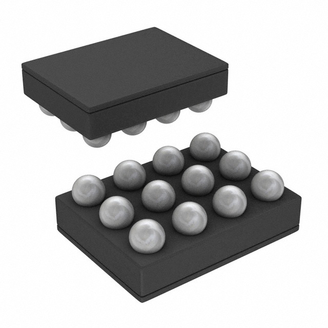
SiP32101, SiP32102, SiP32103
www.vishay.com
Vishay Siliconix
6.5 mΩ, Bi-Directional Battery Switch in Compact WCSP
DESCRIPTION
FEATURES
The SiP32101, SiP32102, and SiP32103 bidirectional
switches feature reverse blocking capability to isolate the
battery from the system. The internal switch has an ultra-low
6.5 mΩ (typ at 3.3 V) on-resistance and operates from a
+2.3 V to +5.5 V input voltage range, making the devices
ideal battery-disconnect switches for high-capacity battery
applications.
•
•
•
•
•
•
•
•
•
Bi-directional ON and OFF
7 A continuous current capability
Ultra low Ron, 6.5 mΩ (typ.) at 3.3 V
Wide input voltage, 2.3 V to 5.5 V
Slew rate controlled turn on
Ultra-low quiescent current: 15 pA (SiP32101, SiP32102)
EN pin with integrated pull up or pull down resistor
Available in both logic high and logic low enable options
Compact 12-Bump, 1.3 mm x 1.7 mm x 0.55 mm
WCSP package
• Material categorization: for definitions of compliance
please see www.vishay.com/doc?99912
The SiP32101, SiP32102, and SiP32103 have slew rate
control, making them ideal in large load capacitor as well as
high-current load switching applications. These devices are
also highly efficient, consuming a mere 10 pA (typ.) current
in shutdown and 15 pA while operating.
The SiP32101 and SiP32103 have an active low enable and
the SiP32102 has an active high enable. They can interface
directly with a low voltage control signal.
APPLICATIONS
•
•
•
•
•
•
•
The SiP32101, SiP32102, and SiP32103 are available in an
ultra compact 12-Bump, 1.3 mm x 1.7 mm, 0.4 mm pitch
WCSP package with top side lamination. The device
operates over the temperature of -40 °C to +85 °C.
Smartphones and tablets
Digital still / video cameras
Portable meters and test instruments
Communication devices with embedded batteries
Portable medical and healthcare systems
Data storage
Battery bank
TYPICAL APPLICATION CIRCUIT
System Charging Block
System Connector
Power Input
Charging
Control
and
Regulator
System Power Input
Charger Output
Port B
Port A
To Battery Pack
Slew Rate Gate
Drive Logic
LevelShift
EN, EN
SiP32101,
SiP32102
GND
Fig. 1 - Typical Application Circuit
ORDERING INFORMATION
PART NUMBER
SiP32101DB-T1-GE1
SiP32102DB-T1-GE1
SiP32102DB-T5-GE1
SiP32103DB-T1-GE1
SiP32101EVB
SiP32102EVB
SiP32103EVB
MARKING
ENABLE
ENABLE PULL RESISTOR
32101
32102
32102
32103
-
Low enable
High enable
High enable
Low enable
-
Pull Low
Pull Low
Pull Low
Pull High
-
PACKAGE
TEMPERATURE
12-Bump, 1.3 mm x 1.7 mm,
0.4 mm pitch
WCSP package
-40 °C to +85 °C
Evaluation Board
-
Note
• GE1 denotes halogen-free and RoHS-compliant
MARKING
1
2
3
4
A
B
FYWL
32101
C
S15-0598-Rev. G, 30-Mar-15
Document Number: 62617
1
For technical questions, contact: powerictechsupport@vishay.com
THIS DOCUMENT IS SUBJECT TO CHANGE WITHOUT NOTICE. THE PRODUCTS DESCRIBED HEREIN AND THIS DOCUMENT
ARE SUBJECT TO SPECIFIC DISCLAIMERS, SET FORTH AT www.vishay.com/doc?91000
�SiP32101, SiP32102, SiP32103
www.vishay.com
Vishay Siliconix
ABSOLUTE MAXIMUM RATINGS
PARAMETER
VPA, VPB
VEN
CONDITIONS
LIMIT
Reference to GND
-0.3 to +6
UNIT
Pulse at 1 ms reference to GND a
-1.6
Reference to GND
-0.3 to +6
100 μs pulse
15
Maximum Continuous Switch Current
V
7
Maximum Pulse Current
ESD (HBM)
A
8000
Operating Temperature
V
-40 to +85
Operating Junction Temperature
125
Storage Temperature
°C
-65 to +150
Thermal Resistance (θJA) b
Power Dissipation (PD) b, c
TA = 70 °C
73
°C/W
1096
mW
Notes
a. Negative current injection up to 300 mA.
b. All bumps soldered to 1 inch x 1 inch, 2 oz. copper, 4 layers PC board.
c. Derate 13.7 mW/°C above TA = 70 °C.
Stresses beyond those listed under "Absolute Maximum Ratings" may cause permanent damage to the device. These are stress ratings only, and functional operation
of the device at these or any other conditions beyond those indicated in the operational sections of the specifications is not implied. Exposure to absolute maximum
rating/conditions for extended periods may affect device reliability.
SPECIFICATIONS
TEST CONDITIONS UNLESS SPECIFIED
SYMBOL VIN = VPA/VPB = 2.3 V to 5.5 V, TA = -40 °C to 85 °C
(Typical values are at VPA, VPB = 4.2 V,
CPA, CPB = 0.1 μF, TA = 25 °C)
PARAMETER
LIMITS
MIN.a
TYP.b
MAX.a
UNIT
Power Supply
Operating Voltage c
VPA/PB
Quiescent Current
IQ
Shutdown Current
ISHDN
2.3
-
5.5
V
VEN = 0 V (for SiP32101),
VEN = VIN (for SiP32102),
no load
-
0.015
300
nA
VEN = 0 V (for SiP32103),
no load
-
8.2
15
μA
VEN = VIN (for SiP32101),
VEN = 0 V (for SiP32102),
no load
-
0.010
300
nA
Internal FET
On-Resistance
RDS(on)
VPA/VPB = 2.3 V, IL = 500 mA, TA = 25 °C
-
8
13
VPA/VPB = 3.3 V, IL = 500 mA, TA = 25 °C
-
6.5
10
mΩ
Control
EN / EN Input Logic-Low Voltage c
VIL
-
-
0.4
Voltage c
VIH
1.4
-
-
-
500
700
EN / EN Input Logic-High
EN / EN Pull Resistor
REN
VPA/VPB = 5.5 V, VEN (or VEN) = 2.3 V
V
kΩ
Timing
Output Turn-On Delay Time
td(on)
-
0.5
-
Output Turn-On Rise Time
tr
-
1
-
Output Turn-Off Delay Time
td(off)
-
2.4
-
-
1
-
Output Turn-Off Fall Time
tf
VIN = 4.2 V, RL = 100 Ω, CL = 0.1 μF, TA = 25 °C
ms
Notes
a. The algebraic convention whereby the most negative value is a minimum and the most positive a maximum.
b. Typical values are for DESIGN AID ONLY, not guaranteed nor subject to production testing.
c. For VIN outside this range consult typical EN, EN threshold curve.
S15-0598-Rev. G, 30-Mar-15
Document Number: 62617
2
For technical questions, contact: powerictechsupport@vishay.com
THIS DOCUMENT IS SUBJECT TO CHANGE WITHOUT NOTICE. THE PRODUCTS DESCRIBED HEREIN AND THIS DOCUMENT
ARE SUBJECT TO SPECIFIC DISCLAIMERS, SET FORTH AT www.vishay.com/doc?91000
�SiP32101, SiP32102, SiP32103
www.vishay.com
Vishay Siliconix
BUMP CONFIGURATION
1
A
2
A1
A2
Port B
B
B1
B2
C1
A4
Port B
B3
Port A
C2
GND
4
A3
Port A
Port B
C
3
B4
Port B
C3
Port A
/EN
Port A
C4
Port B
Port A
Top view (solder bumps on bottom)
Fig. 2 - WCSP12, 1.3 mm x 1.7 mm
BUMP DESCRIPTION
BUMP NUMBER
A1, B1, A3, B3, C3
C1
A2, B2, C2, B4, C4
A4
NAME
FUNCTION
PB
Power port B
GND
Ground
PA
Power port A
EN / EN
Switch enable input,
active low for SiP32101 and SiP32103, active high for SiP32102
FUNCTIONAL BLOCK DIAGRAM
Internal Bias
Circuit
Internal Bias
Circuit
Port A
EN, SiP32101
EN, SiP32102
Port B
Slew Rate Gate
Drive
Logic Level Shift
Port A
EN, SiP32101
Port B
Slew Rate Gate
Drive
Logic Level Shift
SiP32101,
SiP32102
GND
S15-0598-Rev. G, 30-Mar-15
SiP32103
GND
Document Number: 62617
3
For technical questions, contact: powerictechsupport@vishay.com
THIS DOCUMENT IS SUBJECT TO CHANGE WITHOUT NOTICE. THE PRODUCTS DESCRIBED HEREIN AND THIS DOCUMENT
ARE SUBJECT TO SPECIFIC DISCLAIMERS, SET FORTH AT www.vishay.com/doc?91000
�SiP32101, SiP32102, SiP32103
www.vishay.com
Vishay Siliconix
TYPICAL CHARACTERISTICS (internally regulated 25 °C, unless otherwise noted)
0.24
10.00
0.22
IQPA/IQPB - Quiescent Current (nA)
IQPA/IQPB - Quiescent Current (nA)
SiP32101, SiP32102
SiP32101, SiP32102
0.20
0.18
0.16
0.14
0.12
0.10
0.08
0.06
0.04
1.00
VPA/VPB = 5.0 V
0.10
VPA/VPB = 4.2 V
VPA/VPB = 2.7 V
0.02
0.01
- 40
0.00
2.0
2.5
3.0
3.5
4.0
4.5
5.0
5.5
6.0
- 15
Fig. 3 - Quiescent vs. Input Voltage
60
85
16
VEN = 0 V (SiP32103)
VEN = 0 V (SiP32103)
14
IQPA/IQPB - Quiescent Current (μA)
14
IQPA/IQPB - Quiescent Current (μA)
35
Fig. 6 - Quiescent vs. Temperature
16
12
10
8
6
4
2
VPA/VPB = 5.0 V
12
10
8
VPA/VPB = 4.2 V
6
4
VPA/VPB = 2.7 V
2
0
0
2.0
VPA/VPB (V)
10
35
Temperature (°C)
Fig. 4 - Quiescent vs. Input Voltage
Fig. 7 - Quiescent vs. Temperature
2.5
3.0
3.5
4.0
4.5
5.0
5.5
- 40
6.0
0.12
- 15
60
85
10
VEN = VPA/VPB (SiP32101, SiP32102)
IL = 0.5 A
VPA/VPB = 4.2 V
9
0.10
RDS - On-Resistance (mΩ)
ISHDN-PA/ISHDN-PB - Shutdown Current (nA)
10
Temperature (°C)
VPA /VPB (V)
0.08
0.06
0.04
0.02
8
7
6
5
4
3
2
0.00
2.0
2.5
3.0
3.5
4.0
4.5
5.0
5.5
VPA /VPB (V)
Fig. 5 - Shutdown Current vs. Input Voltage
S15-0598-Rev. G, 30-Mar-15
6.0
- 40
- 15
10
35
60
85
Temperature (°C)
Fig. 8 - On Resistance vs. Temperature
Document Number: 62617
4
For technical questions, contact: powerictechsupport@vishay.com
THIS DOCUMENT IS SUBJECT TO CHANGE WITHOUT NOTICE. THE PRODUCTS DESCRIBED HEREIN AND THIS DOCUMENT
ARE SUBJECT TO SPECIFIC DISCLAIMERS, SET FORTH AT www.vishay.com/doc?91000
�SiP32101, SiP32102, SiP32103
www.vishay.com
Vishay Siliconix
TYPICAL CHARACTERISTICS (internally regulated 25 °C, unless otherwise noted)
1.15
RDS(norm) - Normalized On -Resistance
ISHDN-PA/ISHDN-PB - Shutdown Current (nA)
10
1
VPA/VPB = 5 V
0.1
VPA/VPB = 4.2
VPA/VPB = 2.7 V
0.01
- 40
- 15
10
35
60
85
VPA/VPB = 3.3 V
1.1
VPA/VPB = 4.35 V
1.05
VPA/VPB = 5 V
1
0.95
1
0.001
VPA/VPB = 2.7 V
TA = 25 °C
2
3
4
5
6
7
IOUT (A)
Temperature (°C)
Fig. 9 - Shutdown Current vs.Temperature
Fig. 12 - Normalized On Resistance vs. Load Current
0
10
-2
IPB/IPA - Input Current (nA)
RDS - On-Resistance (mΩ)
9
IL = 0.5 A
8
7
6
-4
-6
-8
- 10
- 12
5
VPB/VPA = 2.3 V
- 14
- 16
4
2.0
2.5
3.0
3.5
4.0
4.5
5.0
5.5
2.0
6.0
2.5
3.0
VPA/VPB (V)
4.0
4.5
5.0
5.5
VPA/VPB (V)
Fig. 10 - On Resistance vs. Input Voltage
Fig. 13 - Reverse Blocking Current (IRB) vs. Output Voltage
600
1.30
V EN = 2.3 V
VPA/VPB = 5.5 V
580
560
VPA/VPB = 4.2 V
CL = 0.1 μF
RL = 10 Ω
1.20
540
tr - Rise Time (ms)
R/EN - /EN Pull down / Pull up Resistance (kΩ)
3.5
520
500
480
1.10
1.00
460
0.90
440
420
0.80
400
- 40
- 15
10
35
60
85
Temperature (°C)
Fig. 11 - EN Pull down Resistance vs. Temperature
S15-0598-Rev. G, 30-Mar-15
- 40
- 15
10
35
60
85
Temperature (°C)
Fig. 14 - Rise Time vs. Temperature
Document Number: 62617
5
For technical questions, contact: powerictechsupport@vishay.com
THIS DOCUMENT IS SUBJECT TO CHANGE WITHOUT NOTICE. THE PRODUCTS DESCRIBED HEREIN AND THIS DOCUMENT
ARE SUBJECT TO SPECIFIC DISCLAIMERS, SET FORTH AT www.vishay.com/doc?91000
�SiP32101, SiP32102, SiP32103
www.vishay.com
Vishay Siliconix
TYPICAL CHARACTERISTICS (internally regulated 25 °C, unless otherwise noted)
0.9
3.0
VPA/VPB = 4.2 V
CL = 0.1 μF
RL = 10 Ω
td(off) - Turn-Off Delay Time (ms)
EN, EN - Threshold Voltage (V)
0.85
VIH
0.8
VIL
0.75
0.7
0.65
0.6
2.8
2.6
2.4
2.2
2.0
0.55
1.8
0.5
2.0
3.0
4.0
5.0
- 40
6.0
- 15
35
60
85
Temperature (°C)
VPA / VPB (V)
Fig. 15 - EN, EN Threshold Voltage vs. Input Voltage
Fig. 17 - Turn-off Delay Time vs. Temperature
0.7
1.2
VPA/VPB = 4.2 V
CL = 0.1 μF
0.65
VPA/VPB = 4.2 V
CL = 0.1 μF
RL = 10 Ω
1.1
0.6
tf - Fall Time (ms)
td(on) - Turn-On Delay Time (ms)
10
0.55
0.5
1.0
0.9
0.8
0.7
0.45
0.6
0.4
- 40
- 15
10
35
60
85
- 40
- 15
10
35
60
Temperature (°C)
Temperature (°C)
Fig. 16 - Turn-on Delay Time vs. Temperature
Fig. 18 - Fall Time vs. Temperature
S15-0598-Rev. G, 30-Mar-15
85
Document Number: 62617
6
For technical questions, contact: powerictechsupport@vishay.com
THIS DOCUMENT IS SUBJECT TO CHANGE WITHOUT NOTICE. THE PRODUCTS DESCRIBED HEREIN AND THIS DOCUMENT
ARE SUBJECT TO SPECIFIC DISCLAIMERS, SET FORTH AT www.vishay.com/doc?91000
�SiP32101, SiP32102, SiP32103
www.vishay.com
Vishay Siliconix
DETAILED DESCRIPTION
The SiP32101, SiP32102, and SiP32103 bidirectional
switches feature reverse blocking capability to isolate the
battery from the system. The internal switch has an ultra-low
6.5 mΩ (typ. at 3.3 V) on-resistance and operates from a
+2.3 V to +5.5 V input voltage range, making the device ideal
battery-disconnect switch for high-capacity battery
applications. The parts can handle 7 A continuous current at
both directions.
The SiP32101, SiP32102, and SiP32103 have slew rate
control, making them ideal in large load capacitor as well as
high-current load switching applications.
The SiP32101, SiP32102, and SiP32103 are available in an
ultra compact 12-Bump, 1.3 mm x 1.7 mm, 0.4 mm pitch
WCSP package with top side lamination. The device
operates over the temperature of -40 °C to +85 °C.
)
REVERSE CURRENT BLOCKING
The SiP32101, SiP32102, and SiP32103 are bidirectional
switches that prevent current flowing from either port to the
other when the device is disabled.
Fig. 20 - Port B Turn-Off Time
(VPA = 4.2 V, RL = 10 Ω, CL = 0.1 μF)
EN, EN INPUT
SiP32101 and SiP32103 have an active-low enable pin
which can interface with low voltage GPIO directly. The
switch is on when EN is low and off when EN is high. The
SiP32102 has an active-high enable pin that turns the switch
on when high and off when low. The SiP32101 and
SiP32102 have an integrated pull down resistor at EN pin.
The SiP32103 EN pin integrates a pull up resistor that will
automatically connected to either port A or port whichever
is of higher voltage.
DEVICE PIN OUT
Device pin out is designed for ease of layout.
Port B
/EN
SWITCH ON AND OFF PERFORMANCE
A1
A2
Port B
Current
The SiP32101, SiP32102, and SiP32103 have slew rate
control. This minimizes the inrush current and provides a
soft turn on.
B1
B2
Port B
C1
A4
B3
B4
Port B
C3
Port A
/EN
Port B
Port A
C2
GND
GND
A3
Port A
Port A
C4
Port B
Port A
Port A
Fig. 21 - Proposed Layout
Fig. 19 - Port B Turn-On Time
(VPA = 4.2 V, RL = 10 Ω, CL = 0.1 μF)
Vishay Siliconix maintains worldwide manufacturing capability. Products may be manufactured at one of several qualified locations. Reliability data for Silicon
Technology and Package Reliability represent a composite of all qualified locations. For related documents such as package/tape drawings, part marking, and
reliability data, see www.vishay.com/ppg?62617.
S15-0598-Rev. G, 30-Mar-15
Document Number: 62617
7
For technical questions, contact: powerictechsupport@vishay.com
THIS DOCUMENT IS SUBJECT TO CHANGE WITHOUT NOTICE. THE PRODUCTS DESCRIBED HEREIN AND THIS DOCUMENT
ARE SUBJECT TO SPECIFIC DISCLAIMERS, SET FORTH AT www.vishay.com/doc?91000
�Package Information
www.vishay.com
Vishay Siliconix
WCSP12: 12 Bumps
(3 x 4, 0.4 mm pitch, 208 μm bump height, 1.71 mm x 1.31 mm die size)
Index Bump A1
A3
A2
A1
B4
B3
B2
B1
C4
C3
C2
C1
s
e
D
e
FYWL
ABCDE
A4
s
b
s
E
Top View
e
e
e
e
Note 3
e
e
A1
A
Note 4
Bottom View
A1
e
s
Bump Note 2
Side View
e
RECOMMENDED
LAND PATTERN
(NSMD)
MILLIMETERS (5)
INCHES
DIMENSION
MIN.
NOM.
MAX.
MIN.
NOM.
MAX.
A
0.515
0.530
0.545
0.0203
0.0209
0.0215
A1
0.183
0.208
0.233
0.0072
0.0082
0.0092
b
0.234
0.260
0.312
0.0092
0.0102
0.0123
e
0.400
0.0157
s
0.235
0.255
0.275
0.0093
0.0100
D
1.270
1.310
1.350
0.0500
0.0516
0.0108
0.0531
E
1.670
1.710
1.750
0.0657
0.0673
0.0689
Notes (unless otherwise specified)
(1) Laser mark on the silicon die back coated with an epoxy film.
(2) Bumps are SAC396.
(3) 0.050 max. co-planarity.
(4) Laminate tape thickness is 0.022 mm.
(5) Use millimeters as the primary measurement.
ECN: S13-2510-Rev. B, 16-Dec-13
DWG: 6017
Revision: 16-Dec-13
Document Number: 62592
1
For technical questions, contact: powerictechsupport@vishay.com
THIS DOCUMENT IS SUBJECT TO CHANGE WITHOUT NOTICE. THE PRODUCTS DESCRIBED HEREIN AND THIS DOCUMENT
ARE SUBJECT TO SPECIFIC DISCLAIMERS, SET FORTH AT www.vishay.com/doc?91000
�Legal Disclaimer Notice
www.vishay.com
Vishay
Disclaimer
ALL PRODUCT, PRODUCT SPECIFICATIONS AND DATA ARE SUBJECT TO CHANGE WITHOUT NOTICE TO IMPROVE
RELIABILITY, FUNCTION OR DESIGN OR OTHERWISE.
Vishay Intertechnology, Inc., its affiliates, agents, and employees, and all persons acting on its or their behalf (collectively,
“Vishay”), disclaim any and all liability for any errors, inaccuracies or incompleteness contained in any datasheet or in any other
disclosure relating to any product.
Vishay makes no warranty, representation or guarantee regarding the suitability of the products for any particular purpose or
the continuing production of any product. To the maximum extent permitted by applicable law, Vishay disclaims (i) any and all
liability arising out of the application or use of any product, (ii) any and all liability, including without limitation special,
consequential or incidental damages, and (iii) any and all implied warranties, including warranties of fitness for particular
purpose, non-infringement and merchantability.
Statements regarding the suitability of products for certain types of applications are based on Vishay's knowledge of typical
requirements that are often placed on Vishay products in generic applications. Such statements are not binding statements
about the suitability of products for a particular application. It is the customer's responsibility to validate that a particular product
with the properties described in the product specification is suitable for use in a particular application. Parameters provided in
datasheets and / or specifications may vary in different applications and performance may vary over time. All operating
parameters, including typical parameters, must be validated for each customer application by the customer's technical experts.
Product specifications do not expand or otherwise modify Vishay's terms and conditions of purchase, including but not limited
to the warranty expressed therein.
Hyperlinks included in this datasheet may direct users to third-party websites. These links are provided as a convenience and
for informational purposes only. Inclusion of these hyperlinks does not constitute an endorsement or an approval by Vishay of
any of the products, services or opinions of the corporation, organization or individual associated with the third-party website.
Vishay disclaims any and all liability and bears no responsibility for the accuracy, legality or content of the third-party website
or for that of subsequent links.
Except as expressly indicated in writing, Vishay products are not designed for use in medical, life-saving, or life-sustaining
applications or for any other application in which the failure of the Vishay product could result in personal injury or death.
Customers using or selling Vishay products not expressly indicated for use in such applications do so at their own risk. Please
contact authorized Vishay personnel to obtain written terms and conditions regarding products designed for such applications.
No license, express or implied, by estoppel or otherwise, to any intellectual property rights is granted by this document or by
any conduct of Vishay. Product names and markings noted herein may be trademarks of their respective owners.
© 2021 VISHAY INTERTECHNOLOGY, INC. ALL RIGHTS RESERVED
Revision: 09-Jul-2021
1
Document Number: 91000
�


 工商网监
湘ICP备2023018690号
工商网监
湘ICP备2023018690号
