4Gbit x8: NAND Flash Memory
NAND Flash Memory
(AX20NV4G8)
Features
Interface
Open NAND Flash Interface
(ONFI 1.0) compliant
x8
Technology
Single-level cell (SLC)
1xnm NAND Process
Operating Voltage Range
VCC: 2.70V – 3.60V
Operating Temperature Range
Industrial: -40°C to 85°C
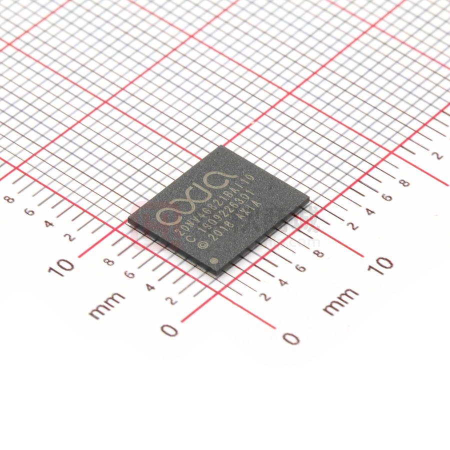
Packages
48-pin TSOP (12mm x 20mm)
63-ball FBGA (9mm x 11mm)
Device Signature
Manufacturer’s ID
Device ID
Device Parameters
Unique ID
Quality and Reliability
Error Correction Code:
1-bit / 544 bytes of data
Data retention: 10 years
Endurance (P/E cycles): 60K (Typ.)
Block zero (block address 00h) is a valid
block when shipped from factory and will
remain valid for at least 1K P/E cycles
with ECC
Memory Array Organization
x8
Page size: 2176 bytes
(2048 + 128 bytes)
Block size: 64 pages
(128K + 8K bytes)
Device size: 4096 blocks (2 Planes)
Firmware SLC Region
Data Protection
Volatile / Non-Volatile
OTP Array: 64 pages of One-TimeProgrammable memory area (1 block)
Device Status
Ready/busy# (R/B#) signal: hardware
method for detecting internal operation
completion status
Advanced Command Set
Page data move (copy back):
Internal data move
Multi-plane Commands
Performance
Device Operation
Values
Units
Single Plane Read
45.0 (Typical)
µs
Multiple Plane Read
55.0 (Typical)
µs
Read Cycle Time
20.0 (Minimum)
ns
Program Page Time
350.0 (Typical)
µs
4.0 (Typical)
ms
Block Erase Time
Standby
Read page
Revision: G
100.0 (Maximum)
µA
25.0 (Typical)
mA
Axia Memory Technology
P a g e 1 | 54
�4Gbit x8: NAND Flash Memory
Table of Contents
Features ...................................................................................................................................................... 1
Performance .............................................................................................................................................. 1
Table of Contents ..................................................................................................................................... 2
General Description................................................................................................................................. 4
Ordering Options ..................................................................................................................................... 5
Valid Combinations — Standard ...................................................................................................... 5
Signal Description and Assignment ................................................................................................... 6
Package Options ...................................................................................................................................... 7
48-Pin TSOP (Top View) ..................................................................................................................... 7
63-Ball FBGA (Balls Down, Top View) ............................................................................................ 8
Architecture ............................................................................................................................................... 9
Memory Array Architecture & Addressing .................................................................................. 10
Configuration Register (Address 90h).......................................................................................... 11
Configuration Register (Address 80h).......................................................................................... 11
Status Register ................................................................................................................................... 12
Block Protection Status Register .................................................................................................. 13
Identification Definition (Address 00h) ........................................................................................ 14
Identification Definition (Address 20h) ........................................................................................ 15
Parameter Page Structure & Values.............................................................................................. 16
Device Protection ................................................................................................................................... 19
Volatile Protection (Temporary) ..................................................................................................... 19
Non-Volatile Protection (Permanent) ............................................................................................ 20
One-Time Programmable (OTP) Region ...................................................................................... 21
Firmware SLC Region ....................................................................................................................... 21
Partial Programming ............................................................................................................................. 22
Bus Interface ........................................................................................................................................... 23
Standby................................................................................................................................................. 23
Busy ....................................................................................................................................................... 23
Command Input .................................................................................................................................. 24
Address Input ...................................................................................................................................... 24
Revision:G
Axia Memory Technology
P a g e 2 | 54
�4Gbit x8: NAND Flash Memory
Data Input ............................................................................................................................................. 25
Data Output.......................................................................................................................................... 25
Command Set ...................................................................................................................................... 26
Device Initialization ............................................................................................................................... 48
Electrical Specifications....................................................................................................................... 49
Error Management ................................................................................................................................. 52
Product Use Limitations....................................................................................................................... 53
Limited Warranty ................................................................................................................................ 53
Revision History ..................................................................................................................................... 54
Revision:G
Axia Memory Technology
P a g e 3 | 54
�4Gbit x8: NAND Flash Memory
General Description
Axia Memory Technology’s AX20NV4Gx is a 3.0V 4Gbit NAND Flash organized as 2176 bytes × 64 pages
× 4096 blocks. All read and program operations are performed using a 2176-byte register; allows data to
be transferred to and from the memory array in 2176-bytes increments. The erase operation is implemented
in a single block unit (2176 bytes × 64 pages). ECC is included for higher data reliability.
Axia’s NAND Flash devices communicate through an asynchronous ONFI 1.0 compatible interface for highperformance I/O operations. It is a multiplexed 8-bit (I/O8) to transfer commands, address, and data. There
are five control signals used to implement the asynchronous data interface: CE#, CLE, ALE, WE#, and
RE#. Additional signals control hardware write protection (WP#) and monitor device status (R/B#). This
hardware interface creates a low pin-count device with a standard pinout that remains the same in Axia’s
NAND device family, enabling future upgrades to higher densities with no board redesign.
Axia’s AX20NV4Gx NAND Flash supports multi-plane program and erase operations. Program operation
with multi-plane structure allows 2 pages to be programmed at a time (one in each plane). Similarly, erase
operation with multi-page structure allows 2 blocks to be erased at a time (one in each plane). This reduces
overall program and erase times compared to similar operations in single-plane structure.
Additionally, Axia’s NAND Flash devices support a copy back function which optimizes management of
defective blocks. When a page program operation fails, the data already loaded in the page buffer can be
directly programmed to another page inside the same array section without the time-consuming serial data
insertion phase.
And finally, Axia’s NAND Flash devices provide special features listed below in Table 1:
Table 1: Special Features
#
1
2
3
Feature Description
One-Time Programmable Area
Unique Identifier
Firmware SLC Region
Revision:G
Details
Size: 1 block (128K + 8K bytes)
Size: 16 bytes
Axia Memory Technology
P a g e 4 | 54
�4Gbit x8: NAND Flash Memory
Ordering Options
The ordering part numbers are firmed by a valid combination of the following options:
Valid Combinations — Standard
Valid Combinations list includes device configurations currently available. Contact your local sales office to
confirm availability of specific valid combinations and to check on newly released combinations.
Table 2: Valid Combinations List
Valid Combinations
Base Part
Number
Bus
Width
Generation
Die
Code
Package
type
Temperature
Range
Special
Features
Packing
Type
Part
Number
AX20NV4G821BAI101
AX20NV4G
x8
2
1
BA, TA
I
10
1, 2
AX20NV4G821TAI101
AX20NV4G821BAI102
Revision:G
Axia Memory Technology
P a g e 5 | 54
�4Gbit x8: NAND Flash Memory
Signal Description and Assignment
Figure 1: Device Pinout
ALE
CE#
WP#
AXIA
RE#
NAND
4Gbit
WE#
I/O[7:0]
CLE
VP
R/B#
Table 3: Signal Description
Signal
Type
Description
CE#
Input
Chip enable: Enables or disables the NAND Flash.
CLE
ALE
Input
Input
Command latch enable: Loads a command from x8 - I/O[7:0] into the command register.
Address latch enable: Loads an address from x8 - I/O[7:0] into the address register.
WE#
Input
RE#
WP#
Input
Input
Write enable: Transfers commands, addresses, and serial data from the host system to
the NAND Flash.
Read enable: Transfers serial data from the NAND Flash to the host system.
Write protect: Enables or disables array PROGRAM and ERASE operations.
VP
Input
R/B#
Output
I/O [7:0] - x8
Input/Output
VCC
Supply
VCC: Core and I/O power supply.
VSS
Supply
VSS: Core and I/O ground supply.
NC
Revision:G
Volatile protect: Enables or disables block granular array PROGRAM and ERASE
operations. Has a weak internal pull-down to disable protection if the input is left floating.
Ready/busy: An open-drain, active-low output that requires an external pull-up resistor.
This signal indicates NAND Flash activity.
Data inputs/outputs: The bidirectional I/Os transfer address, data, and command
information.
Not Connected: NCs are not internally connected. They can be driven or left
unconnected.
Axia Memory Technology
P a g e 6 | 54
�4Gbit x8: NAND Flash Memory
Package Options
48-Pin TSOP (Top View)
Figure 2: 48-Pin TSOP Pinout and Dimensions
Revision:G
1
48
NC
text
text
NC
NC
text
text
NC
NC
text
text
NC
NC
text
text
NC
NC
text
text
IO7
NC
text
text
IO6
R/B#
text
text
IO5
RE#
text
text
IO4
CE#
text
text
NC
NC
text
text
NC
NC
text
text
VP
VCC
text
12
37
text
VCC
VSS
text
13
36
text
VSS
NC
text
text
NC
NC
text
text
NC
CLE
text
text
NC
ALE
text
text
IO3
WE#
text
text
IO2
WP#
text
text
IO1
NC
text
text
IO0
NC
text
text
NC
NC
text
text
NC
NC
text
text
NC
NC
text
text
NC
48-Pin
TSOP
Package
(x8)
24
25
Axia Memory Technology
P a g e 7 | 54
�4Gbit x8: NAND Flash Memory
63-Ball FBGA (Balls Down, Top View)
Figure 3: 63-Ball FBGA Pinout and Dimensions
Revision:G
Axia Memory Technology
P a g e 8 | 54
�4Gbit x8: NAND Flash Memory
Architecture
Axia’s NAND Flash devices use ONFI 1.0 compatible interface for all operations. Data, commands, and
addresses are multiplexed onto the I/O pins. The commands received at the I/Os are latched into a
command register and are used to determine the operations the device must perform. The addresses are
latched into an address register and sent either to a row decoder to select a row address, or to a column
decoder to select a column address. Data is transferred to or from the NAND Flash memory array either in
a byte format (x8) through a page buffer (data buffer). The NAND Flash memory array is programmed and
read using page-based operations and is erased using block-based operations. The status register reports
the status of all operations.
Axia’s NAND Flash devices offer a protected, one-time programmable (OTP) NAND Flash memory area.
64 full pages (2176 bytes per page) of OTP data are available on the device and the entire range is
guaranteed to be good. The OTP area is accessible only through the OTP commands. Customers can use
the OTP area any way they choose for permanent data storage. The OTP area leaves the factory in an
unwritten state (all bits are 1s). Programming or partial-page programming enables the user to program 0
bits in the OTP area. The OTP area cannot be erased. Protecting the OTP area prevents further
programming of the area.
Figure 4: Functional Block Diagram
Address Register
x8
IO[7:0]
Status Register
I/O
Control
Column
Decoder
ALE
CE#
WP#
RE#
CLE
WE#
VP
Command
&
Control
R/B#
RDY_BSY#
Row Decoder
Command Register
High Voltage Generator
NAND
Memory
Array
(2 Planes)
OTP Area
Page Buffer
Revision:G
Axia Memory Technology
P a g e 9 | 54
�4Gbit x8: NAND Flash Memory
Memory Array Architecture & Addressing
Figure 5: Memory Array Architecture
Plane of Even Numbered
Blocks
Page
Buffer
Plane of Odd Numbered
Blocks
x8:
Page = 2,048 + 128 bytes = 2,176 bytes
1 block = 64 pages (139,264 bytes)
4Gbit Device = 4096 blocks (570,425,344 bytes)
Block 0
Block 1
Block 2
Block 3
……...
……...
Block 4092
Block 4093
Block 4094
Block 4095
Data Buffer
Data Buffer
x8 – 2048 Bytes
x8 – 2048 Bytes
x8 – 128 Bytes
x8 – 128 Bytes
Table 4: Array Addressing Sequence – x8
x8:
Cycle
IO[7]
IO[6]
IO[5]
IO[4]
IO[3]
IO[2]
IO[1]
IO[0]
First
BYTA7
BYTA6
BYTA5
BYTA4
BYTA3
BYTA2
BYTA1
BYTA0
Second
Logic '0'
Logic '0'
Logic '0'
Logic '0'
BYTA11
BYTA10
BYTA9
BYTA8
Third
BA7
BA6 / PLA
PA5
PA4
PA3
PA2
PA1
PA0
Fourth
BA15
BA14
BA13
BA12
BA11
BA10
BA9
BA8
Logic '0'
Logic '0'
Logic '0'
Logic '0'
BA19
BA18
BA17
BA16
Fifth
Notes:
1.
2.
3.
BYTAx: Byte based Column address, WRDAx: Word based Column address, PAx: Page address, BAx: Block address,
PLA: Plane address
Block address concatenated with page address = actual page address
1st and 2nd address cycles form the column Address, whereas 3rd, 4th and 5th address cycles form the row address
Table 5: Block Address
Row Address
000000h ~ 00003Fh
000040h ~ 00007Fh
000080h ~ 0000BFh
0000C0h ~ 0000FFh
•••
03FF40h ~ 03FF7Fh
03FF80h ~ 03FFBFh
03FFC0h ~ 03FFFFh
Revision:G
Axia Memory Technology
Block Number
Block 0 (Plane 0)
Block 1 (Plane 1)
Block 2 (Plane 0)
Block 3 (Plane 1)
•••
Block 4093 (Plane 1)
Block 4094 (Plane 0)
Block 4095 (Plane 1)
P a g e 10 | 54
�4Gbit x8: NAND Flash Memory
Configuration Register (Address 90h)
Table 6: Configuration Register 1 (90h) Definition
Status Register
Bits
Name
CR[7]
RSVD
Reserved for Future Use
0
Reserved for Future Use
CR[6]
RSVD
Reserved for Future Use
0
Reserved for Future Use
CR[5]
RSVD
Reserved for Future Use
0
Reserved for Future Use
CR[4]
ECCM
0
CR[3]
RSVD
On-Die ECC Mode
Configuration
Reserved for Future Use
1
CR[2]
RSVD
Reserved for Future Use
0
0 = Mode 1
1 = Mode 2
Reserved for Future Use
Note: This bit must always be set to Logic 1 (High)
Reserved for Future Use
CR[1]
OTPEP
OTP Area Entry and
Protection
00
CR[0]
Notes:
1.
Function
Default
State
Description
00: OTP Area Not Selected
01: OTP Area Selected (Entry)
10: Reserved
11: OTP Area Protected from Programming (Locked)
CR[4] – ECCM: This bit configures the internal ECC Mode of operation.
a. Mode 1: This mode indicates if a page has a high ECC error count and is recommended to rewrite the page. If set to
‘1’, it is recommended to rewrite the entire page. If cleared to ‘0’, it is in normal state (internal ECC enabled, error
counts are in safe level).
b. Mode 2: This mode indicates if the page has more ECC errors than the internal engine can correct (UECC). If set to
‘1’, it indicates that the ECC has failed and the page is uncorrectable. If cleared to ‘0’, then it is in normal state (internal
ECC enabled, safely working).
Configuration Register (Address 80h)
Table 7: Configuration Register 2 (80h) Definition
Status Register
Bits
Name
Function
CR[7]
RSVD
Reserved for Future Use
0
Reserved for Future Use
CR[6]
RSVD
Reserved for Future Use
0
Reserved for Future Use
CR[5]
RSVD
Reserved for Future Use
0
Reserved for Future Use
0
Reserved for Future Use
CR[4]
RSVD
Reserved for Future Use
CR[3]
IODRV
I/O Drive Strength
Configuration
CR[2]
CR[1]
CR[0]
Revision:G
Default
State
0000
Description
0000: 18Ω – Full Strength
0001: 25Ω – 75% of Full Strength
0010: 35Ω – 50% of Full Strength
0011: 50Ω – 25% of Full Strength
0100 – 1111: Reserved for Future Use
Axia Memory Technology
P a g e 11 | 54
�4Gbit x8: NAND Flash Memory
Status Register
Table 8: Status Register Definition
Status Register
Bits
Name
SR[7]
WRPT
SR[6]
Function
Default
State
Description
WP# based Device
Protection
1
0 = Device is protected - WP# is Low
1 = Device Is not protected - WP# is High
RDY
Device Ready Status Bit
1
0 = Device is busy - not ready
1 = Device is not busy - ready
SR[5]
ARDY
1
SR[4]
ECCS
SR[3]
OTPS
0 = Memory Array is busy - not ready
1 = Memory Array is not busy - ready
0 = Error Count Normal
1 = Page Uncorrectable / Recommend Re-program
0 = OTP Area not protected
1 = OTP Area protected
SR[2]
RSVD
Memory Array Ready
Status Bit
Error Correction Code
(ECC) Status
One-Time
Programmable (OTP)
Area Protection Status
Reserved for Future Use
0
Reserved for Future Use
SR[1]
RSVD
Reserved for Future Use
0
Reserved for Future Use
SR[0]
PES
Program and Erase
Status of the Current
Command
0
0 = Program or Erase was successful
1 = Program or Erase was not successful
Notes:
1.
2.
3.
4.
5.
6.
0
0
SR[7] – WRPT: If set to ‘1’, the device is not write protected and can be programmed or erased. If cleared to ‘0’, then the
device is write protected and cannot be programmed or erased. This is always valid regardless of state of the R/B#.
SR[6] - RDY: If set to ‘1’, the device is ready for another command and all other status bits are valid. If cleared to ‘0’, then
the last command issued is not yet complete and all other status bits are not valid.
SR[5] – ARDY: If set to ‘1’, all array operations are complete. If cleared to zero, then there is a command being processed
or an array operation in progress.
SR[4] – ECCS: If the internal ECC is On, this bit indicates if the last read contained ECC errors. It is supported in two modes;
selected using configuration register address 90h bit [4].
a. Mode 1: This mode indicates if a page has a high ECC error count and is recommended to rewrite the page. If set to
‘1’, it is recommended to rewrite the entire page. If cleared to ‘0’, it is in normal state (internal ECC enabled, error
counts are in safe level).
b. Mode 2: This mode indicates if the page has more ECC errors than the internal engine can correct (UECC). If set to
‘1’, it indicates that the ECC has failed and the page is uncorrectable. If cleared to ‘0’, then it is in normal state (internal
ECC enabled, safely working).
SR[3] – OTPS: This bit indicates whether the OTP is in protected mode (locked down). This bit is set to ‘1’ if the OTP is
locked down and a program command is issued. It is cleared to ‘0’ when either not in OTP mode, or power-up or when
Reset command is issued.
SR[0] – PES: This bit is valid for program and erase operations and shows whether the operation was a success or a failure.
For two plane operation, it indicates that one or both planes failed.
Revision:G
Axia Memory Technology
P a g e 12 | 54
�4Gbit x8: NAND Flash Memory
Block Protection Status Register
Table 9: Block Protection Status Register Definition
Status
Register
Bits
BSR[7]
Name
Function
Default
State
RSVD
Reserved for Future Use
0
Reserved for Future Use
BSR[6]
RSVD
Reserved for Future Use
0
Reserved for Future Use
BSR[5]
RSVD
Reserved for Future Use
0
Reserved for Future Use
BSR[4]
PBLS
0
BSR[3]
BPLS
BSR[2]
BVLS
Permanent Block Lock
Status
Block Permanent Lock
Status
Block Volatile Lock
Status
0 = Permanent Block Lock Disabled (Not Locked Down)
1 = Permanent Block Lock Enabled (Locked Down)
0 = Addressed Block is Protected (Locked)
1 = Addressed Block is not Protected (Not Locked)
000: Reserved
001: Addressed Block is Protected (Locked down)
010: Addressed Block is Protected (Locked)
011: Reserved
100: Reserved
101: Addressed Block is not Protected (Not Locked),
Volatile Protection Enabled (Locked Down)
110: Addressed Block is not Protected (Not Locked),
Volatile Protection Disabled (Not Locked Down)
111: Reserved
BSR[1]
BSR[0]
Revision:G
1
110
Description
Axia Memory Technology
P a g e 13 | 54
�4Gbit x8: NAND Flash Memory
Identification Definition (Address 00h)
Table 10: Device Identification Definition (Address 00h)
Byte
#
0
1
2
Options
Manufacturer's
ID
Device ID
Device
Characteristics
Value
0
Bit
0
1
0
0
DCh
Internal Device # 1
0
0
Internal Device # 2
0
1
Internal Device # 4
1
0
x8
↓
00h
Internal Device # 8
1
1
Page Size - 1KB
0
0
Page Size - 2KB
0
1
Page Size - 4KB
1
0
Page Size - 8KB
1
1
MID
4Gbit, x8, 3.3V
Array
Architecture
Interface Type
4
Number of
Planes
Revision:G
Bit
6
0
Bit
5
1
Bit
4
0
Bit
3
1
Bit
2
1
Bit 1
1
1
0
1
1
1
Cell Type - 2 LEVEL
0
0
Cell Type - 4 LEVEL
0
1
Cell Type - 8 LEVEL
1
0
Cell Type - 16 LEVEL
1
1
Simultaneous Programmed
Pages - 1
Simultaneous Programmed
Pages - 2
Simultaneous Programmed
Pages - 4
Simultaneous Programmed
Pages - 8
Interleaved Programming Not Supported
Interleaved Programming Supported
Cache Program - Not
Supported
Cache Program - Supported
3
Bit
7
1
0
0
0
1
1
0
1
1
ADh
0
1
0
1
Spare Area Size - 64 bytes
per 2048 bytes
Spare Area Size - 128 bytes
per 2048 bytes
Spare Area Size - 256 bytes
per 2048 bytes
Spare Area Size - 512 bytes
per 2048 bytes
Block Size - 128KB
0
0
0
1
1
0
1
1
0
0
0
Block Size - 256KB
0
0
1
Block Size - 512KB
0
1
0
Block Size - 1024KB
0
1
1
1 Plane
0
0
2 Planes
0
1
x8
0
x16
1
Axia Memory Technology
x8
↓
05h
x8
↓
P a g e 14 | 54
�4Gbit x8: NAND Flash Memory
Byte
#
Options
Reserved
4 Planes
Bit
3
1
Bit
2
0
8 Planes
1
1
Reserved for Future Use
Bit
7
0
Bit
6
0
Bit
5
0
Bit
4
0
Bit 1
Bit
0
Value
04h
0
0
Identification Definition (Address 20h)
Table 11: Device Identification Definition (Address 20h)
Byte #
Option
Value
0
1
2
3
"O"
"N"
"F"
"I"
4Fh
4Eh
46h
49h
Revision:G
Axia Memory Technology
P a g e 15 | 54
�4Gbit x8: NAND Flash Memory
Parameter Page Structure & Values
Table 12: Parameter Page Structure & Values
Byte #
O/M
Description
Values
Revision Information & Features Block
0-3
M
Signature "O" "N" "F" "I"
4Fh, 4Eh, 46h, 49h
4-5
M
Revision Number
02h, 00h
6-7
M
Features Supported
Bit #
Value
0
1 = Supports 16-bit Data bus
1
1 = Supports multiple LUN operations
2
1 = Supports non-sequential page
programming
3
1 = Supports interleaved operations
4
1 = Supports odd to even page
Copy Back
5 - 15
0 = Reserved
1Eh, 00h
8-9
M
Optional Commands Supported
Bit #
Value
0
1 = Supports Page Cache Program
1
1 = Supports Read Cache
2
1 = Supports Get/Set features
3
1 = Supports Read Status Enhanced
4
1 = Supports Copy back
5
1 = Supports Read Unique ID
6 - 15
0 = Reserved
3Ch, 00h
Reserved (0)
00h, 00h, 00h, 00h, 00h, 00h,
00h, 00h, 00h, 00h, 00h, 00h,
00h, 00h, 00h, 00h, 00h, 00h,
00h, 00h, 00h, 00h
10- 31
Manufacturer's Information Block
32 - 43
M
Manufacturer's ID (12 ASCII Characters)
53h, 4Bh, 48h, 59h, 4Eh, 49h,
58h, 20h, 20h, 20h, 20h, 20h
44 - 63
M
Device Model (20 ASCII Characters)
48h, 32h, 37h, 55h, 34h, 47h,
38h, 46h, 32h, 47h, 44h, 41h,
2Dh, 42h, 49h, 20h, 20h, 20h,
20h, 20h
64
M
JEDEC Manufacturer's ID
ADh
65 - 66
O
Date Code
00h, 00h
Reserved (0)
00h, 00h, 00h, 00h, 00h, 00h,
00h, 00h, 00h, 00h, 00h, 00h, 00h
67 - 79
Memory Organization Block
80 - 83
M
Number of Data Bytes per Page (2048 Bytes)
00h, 08h, 00h, 00h
84 - 85
M
Number of Spare Bytes per Page (128 Bytes)
80h, 00h
86 - 89
M
Number of Data Bytes per Partial Page (512 Bytes)
00h, 02h, 00h, 00h
90 - 91
M
Number of Spare Bytes per Partial Page (32 Bytes)
20h, 00h
92 - 95
M
Number of Pages per Block (64 Pages)
40h, 00h, 00h, 00h
96 - 99
M
Number of Blocks per Logical Unit (LUN) (4096)
00h, 10h, 00h, 00h
100
M
Number of Logical Units (LUNs)
01h
Revision:G
Axia Memory Technology
P a g e 16 | 54
�4Gbit x8: NAND Flash Memory
Byte #
O/M
101
M
Number of address cycles
Bit #
Value
0-3
Row Address Cycles
4-7
Column Address Cycles
23h
102
M
Number of Bits per Cell
01h
103 - 104
M
Bad Blocks Number per LUN (80)
50h, 00h
105 - 106
M
Block Endurance
60h, EAh
107
M
Guaranteed Valid Blocks at Beginning of Target
00h
108 - 109
M
Block Endurance for Guaranteed Valid Blocks
60h, EAh
110
M
Number of Programs per Page
04h
111
M
Partial Programming Attributes
Bit #
Value
0
1 = Partial Page programming has
Constraints
1-3
1 = Reserved (0)
4
1 = Partial Page Layout
5-7
0 = Reserved
10h
112
M
Number of Bits ECC Correctability
01h
113
M
01h
114
M
Number of Interleaved Address Bits
Bit #
Value
0-3
Number of Interleaved Address Bits
4-7
Reserved (0)
Interleaved Operation Attributes
Bit #
Value
0
Overlapped / concurrent Interleaving
Support
1
1 = No Block Address Restrictions
2
1 = Program Cache Supported
3
Address Restrictions for Program
Cache
4-7
0 = Reserved
Reserved (0)
00h, 00h, 00h, 00h, 00h, 00h,
00h, 00h, 00h, 00h, 00h, 00h, 00h
115 - 127
Description
Values
00h
Electrical Parameter Block
128
M
I/O Pin Capacitance (10pF)
00h
129 - 130
M
Timing Mode Support
Bit #
Value
0
1 = Supports Timing mode 0
1
1 = Supports Timing mode 1
2
1 = Supports Timing mode 2
3
1 = Supports Timing mode 3
4
1 = Supports Timing mode 4
5
1 = Supports Timing mode 5
6 - 15
0 = Reserved
00h, 00h
131 - 132
M
Program Cache Timing Mode Support
Bit #
Value
0
1 = Supports Timing mode 0
1
1 = Supports Timing mode 1
2
1 = Supports Timing mode 2
3
1 = Supports Timing mode 3
4
1 = Supports Timing mode 4
5
1 = Supports Timing mode 5
6 - 15
0 = Reserved
00h, 00h
Revision:G
Axia Memory Technology
P a g e 17 | 54
�4Gbit x8: NAND Flash Memory
Byte #
O/M
133 - 134
M
tPROG Maximum Page Program Time (μs)
Description
58h, 02h
Values
135 - 136
M
tBERS Maximum Block Erase Time (μs)
10h, 27h
137 - 138
M
tR Maximum Page Read Time (μs)
C2h, 01h
139 - 140
tCCS Minimum Change Column Setup Time (ns)
C8h, 00h
141 - 163
Reserved (0)
00h, 00h, 00h, 00h, 00h, 00h,
00h, 00h, 00h, 00h, 00h, 00h,
00h, 00h, 00h, 00h, 00h, 00h,
00h, 00h, 00h, 00h, 00h
Vendor Block
164 - 165
M
166 - 253
254 - 255
M
Vendor Specific Revision Number
00h, 00h
Vendor Specific
00h, 00h, 00h, 00h, 00h, 00h,
00h, 00h, 00h, 00h, 00h, 00h,
00h, 00h, 00h, 00h, 00h, 00h,
00h, 00h, 00h, 00h, 00h, 00h,
00h, 00h, 00h, 00h, 00h, 00h,
00h, 00h, 00h, 00h, 00h, 00h,
00h, 00h, 00h, 00h, 00h, 00h,
00h, 00h, 00h, 00h, 00h, 00h,
00h, 00h, 00h, 00h, 00h, 00h,
00h, 00h, 00h, 00h, 00h, 00h,
00h, 00h, 00h, 00h, 00h, 00h,
00h, 00h, 00h, 00h, 00h, 00h,
00h, 00h, 00h, 00h, 00h, 00h,
00h, 00h, 00h, 00h, 00h, 00h,
00h, 00h, 00h, 00h
Integrity CRC
F9h, 0Ah
Redundant Parameter Pages
256 - 511
M
Value of Bytes 0 - 255
Not Available
512 - 767
M
Value of Bytes 0 - 255
Not Available
768 +
O
Additional Redundant Parameter Pages
Not Available
Revision:G
Axia Memory Technology
P a g e 18 | 54
�4Gbit x8: NAND Flash Memory
Device Protection
Write Protect WP#
The write protect# (WP#) signal enables or disables PROGRAM and ERASE operations within the Flash
device. When WP# is Low, PROGRAM and ERASE operations are disabled. When WP# is High,
PROGRAM and ERASE operations are enabled.
It is recommended that the host drive WP# Low during power-on until VCC is stable to prevent inadvertent
PROGRAM and ERASE operations.
WP# must be transitioned only when the device is in Standby and prior to beginning a command sequence.
After a command sequence is complete and the device is ready, WP# can be transitioned. After WP# is
transitioned, the host must wait tWW before issuing a new command.
The WP# signal is always an active input, even when CE# is High. This signal should not be multiplexed
with other signals.
Volatile Protection (Temporary)
The volatile protection also enables or disables PROGRAM and ERASE operations, however, the
protection is temporary. Power cycling resets the protection settings to the default status (all
blocks are protected if VP pin is High).
The Volatile Protection method can protect all blocks or a selected range of continuous blocks
from PROGRAM and ERASE operations. The block range is selected by issuing a set of
commands which consist of specifying a Lower Boundary Address and an Upper Boundary
Address to unprotect – remember when VP pin is High after a power cycle, all blocks are
protected. The VP pin’s input level is latched during power-up and determines whether the Volatile
Protection is enabled or disabled.
The block range to protect from PROGRAM and ERASE operations is selected using Unlock
Block commands (23h and 24h). The Unlock Block Lower command (23h) sets the lower block
address and must be followed by the Unlock Block Upper command (24h) to sets the upper block
address. This address range is now unprotected – PROGRAM and ERASE operations are
enabled. Any blocks that lie outside this range are protected. These unprotected blocks can be
protected again by issuing the Lock All Blocks Volatile (2Ah) command. Selecting the range of
blocks to unlock (unprotect) can be followed by a Lock Down Volatile command (2Ch) to set the
Volatile Protection until the next power-down cycle. Following the Lock Down Volatile command,
the device ignores the status of the VP pin and all further Volatile Protection command till the next
power cycle.
The device does offer the option to unprotect the complementary range of blocks. This is achieved
by setting an invert-bit in the Unlock command address field. If the invert-bit is set to Logic ‘0’, the
unprotected area is within and inclusive of the upper and lower block addresses; if the bit is set
to Logic ‘1’, the un-protected area is outside and exclusive of the upper and lower block
addresses.
Revision:G
Axia Memory Technology
P a g e 19 | 54
�4Gbit x8: NAND Flash Memory
Table 13: Volatile protection Unlock Addressing Sequence – x8
x8:
Cycle
IO[7]
IO[6]
IO[5]
IO[4]
IO[3]
IO[2]
IO[1]
IO[0]
First
BA[1]
BA[0]/PLA
Logic '0'
Logic '0'
Logic '0'
Logic '0'
Logic '0'
Invert Bit
Second
Third
Notes:
1.
2.
BA[9]
BA[8]
BA[7]
BA[6]
BA[5]
BA[4]
BA[3]
BA[2]
Logic '0'
Logic '0'
Logic '0'
Logic '0'
BA[13]
BA[12]
BA[11]
BA[10]
BAx: Block address, PLA: Plane address
The invert bit is set by 24h command to select whether the unprotected range is inside or outside of the
range boundary. The bit is DON’T CARE for 23h command.
Figure 6: Volatile Protection range Options
Invert Bit = 0
Invert Bit = 1
Locked Blocks
Unlocked Blocks
Unlocked Blocks
Locked Blocks
Locked Blocks
Unlocked Blocks
Upper Boundary
Address
Lower Boundary
Address
Non-Volatile Protection (Permanent)
The non-volatile protection enables or disables PROGRAM and ERASE operations, however, the
protection is permanent. Multiple groups of blocks can be protected at the same time. Once a
group of blocks is protected, it can no longer be unprotected.
The non-volatile protection method can protect up to 64 blocks (0 to 63) organized in groups of 4
contiguous blocks. The Program Non-Volatile command sequence (4Ch-03h-1Dh-41h-80h) is
used for enabling the protection. Selecting the group of blocks to protect can be followed by a
Lock Down Non-volatile command sequence (4Ch-03h-1Dh-41h-80h). When this Lock Down
Non-volatile command sequence is issued, all groups of blocks protected by non-volatile
protection are permanently protected from program and erase operations and a non-volatile block
protection command sequence can no longer be used to protect additional groups. The nonvolatile protection settings are maintained after a power cycle.
The group of blocks being protected is determined by the hex value (y) in the fourth address cycle.
Moreover, non-volatile block protection command sequence can only be issued for a maximum
of 16 times - thus if the y value or a protected group is selected twice, then there is a group that
would not be protected.
Revision:G
Axia Memory Technology
P a g e 20 | 54
�4Gbit x8: NAND Flash Memory
Table 14: Block Group Protection Scheme – Fourth Address Cycle Value
Y Value
0000
0001
0010
0011
0100
0101
0110
0111
1000
1001
1010
1011
1100
1101
1110
1111
Protected Group
0
1
2
3
4
5
6
7
8
9
10
11
12
13
14
15
Blocks Protected
0,1,2,3
4,5,6,7
8,9,10,11
12,13,14,15
16,17,18,19
20,21,22,23
24,25,26,27
28,29,30,31
32,33,34,35
36,37,38,39
40,41,42,43
44,45,46,47
48,49,50,51
52,53,54,55
56,57,58,59
60,61,62,63
One-Time Programmable (OTP) Region
The One-Time Programmable (OTP) Region is a single block (64 pages) which can be
programmed only once. The OTP region does not support ERASE operations. There are two
ways to access the OTP region; OTP AREA ENTRY command sequence (29h-17h-04h-19h) or
by issuing PROGRAM CONFIGURATION REGISTERS (EFh) command with address 90h and
setting the OTPEP bits to ‘0b01’. To exit the OTP region, a RESET command (FFh) must be
entered. If OTP sequence is detected, on-die ECC engine is automatically disabled. Once in the
OTP region, Program Page and Read Page commands are used to access the information.
Once the data in the OTP region is programmed, there is an option to protect the OTP region
from any further programming operations. By issuing the OTP Protection sequence 4Ch-03h1Dh-41h-80h, the OTPEP bits in the Configuration register are set to ‘0b11’ - OTP Area Protected
from Programming (Locked).
The OTP area is mapped to the Block address shown in Table 15 when OTP AREA ENTRY
command sequence is executed.
Table 15: OTP Block Address
Block 06
Address
000180h ~ 0001BF
Firmware SLC Region
The Firmware SLC region is used for storing Firmware codes for controller management. The
Firmware SLC region is accessed by entering Firmware SLC Region Entry command (DAh). To
exit the Firmware SLC region, a RESET command (FFh) must be entered. Once in the Firmware
SLC region, Program Page and Read Page commands are used to access the information.
Revision:G
Axia Memory Technology
P a g e 21 | 54
�4Gbit x8: NAND Flash Memory
Partial Programming
As mentioned before, programming is page based. However, the device does allow multiple
partial page programming within the same page – a minimum of 32 bytes up to a maximum of
2176 consecutive bytes in a single program cycle. The basic programming unit is 32 bytes with
an associated 1 ECC syndrome. The number of consecutive partial page programming operations
(NOP) within the same page must not exceed 4. As an example, 2 programming operations for
the main array (1x512 bytes) and 2 programming operations for spare array (1x32bytes). Main
array data shall be stored in main array region, and the corresponding spare data in the spare
array region. Both main array data and spare array data must be input for each NOP operation.
It is imperative that for each NOP, column address must match up correct NOP’s main array
region with the NOP’s spare region.
During NOP programming, random data input is used to change the column address. There are
4 spare array regions matching the number of NOPs. Main array data is also divided using NOPs.
Table 16 shows the 32-byte addresses for the 4 NOPs.
Table 16: NOP Column Address table
NOP0
0
1
2
3
4
5
6
7
8
9
10
11
12
13
14
15
SPARE0
Column
Address
(Hex)
000~01F
020~03F
040~05F
060~07F
080~09F
0A0~0BF
0C0~0DF
0E0~0FF
100~11F
120~13F
140~15F
160~17F
180~19F
1A0~1BF
1C0~1DF
1E0~1FF
800~81F
Revision:G
NOP1
0
1
2
3
4
5
6
7
8
9
10
11
12
13
14
15
SPARE1
Column
Address
(Hex)
200~21F
220~23F
240~25F
260~27F
280~29F
2A0~2BF
2C0~2DF
2E0~2FF
300~31F
320~33F
340~35F
360~37F
380~39F
3A0~3BF
3C0~3DF
3E0~3FF
820~83F
NOP2
0
1
2
3
4
5
6
7
8
9
10
11
12
13
14
15
SPARE2
Column
Address
(Hex)
400~41F
420~43F
440~45F
460~47F
480~49F
4A0~4BF
4C0~4DF
4E0~4FF
500~51F
520~53F
540~55F
560~57F
580~59F
5A0~5BF
5C0~5DF
5E0~5FF
840~85F
Axia Memory Technology
NOP3
0
1
2
3
4
5
6
7
8
9
10
11
12
13
14
15
SPARE3
Column
Address
(Hex)
600~61F
620~63F
640~65F
660~67F
680~69F
6A0~6BF
6C0~6DF
6E0~6FF
700~71F
720~73F
740~75F
760~77F
780~79F
7A0~7BF
7C0~7DF
7E0~7FF
860~87F
P a g e 22 | 54
�4Gbit x8: NAND Flash Memory
Bus Interface
As mentioned above, the I/O bus on the device is multiplexed. Commands, addresses and data input/output
all share the same I/O pins. Commands and addresses are always supplied on I/O[7:0]. Data uses I/O[7:0]
for x8 configuration.
The read, program or erase command sequences typically consist of a command input cycle, two or five
address input cycles, and one or more data cycles, either input or output.
Table 17: Device Modes Selection
Mode
CE#
CLE
ALE
WE#
RE#
WP#
I/O[x]
Standby
VIH
VIH / VIL
VIH / VIL
VIH / VIL
VIH / VIL
VCC / VSS
VIH / VIL
Command Input
VIL
VIH
VIL
↑
VIH
VIH
Data
Address Input
VIL
VIL
VIH
↑
VIH
VIH
Data
Data Input
VIL
VIL
VIL
↑
VIH
VIH
Data
Data Output
VIL
VIL
VIL
VIH
↓
VIH / VIL
Data
Write Protect
VIH / VIL
VIH / VIL
VIH / VIL
VIH / VIL
VIH / VIL
VIL
VIH / VIL
Notes:
1.
VIH = High (Logic ‘1’), VIL = Low (Logic ‘0’)
Standby
The device enters standby when CE# pin is driven VIH (High). This helps reduce power consumption. In
standby mode, all I/Os are tri-stated (High-Z).
Note: The device enters standby if CE# goes High and the device is not busy (no program/erase operations
in progress).
Busy
The device enters busy when program, erase or read operations are initiated. The device returns to Standby
after the completion of the operation. During busy state, only RESET (FFH) and READ STATUS
REGISTER (70h) commands are accepted by the device.
Table 18: Recommended Signal Selections During Busy
Mode
CE#
CLE
ALE
WE#
RE#
WP#
I/O[x]
VIL
VIL
VIL
VIH
VIH
VIH / VIL
Data
Busy Period (Program)
VIH / VIL
VIH / VIL
VIH / VIL
VIH / VIL
VIH / VIL
VIH
VIH / VIL
Busy Period (Erase)
VIH / VIL
VIH / VIL
VIH / VIL
VIH / VIL
VIH / VIL
VIH
VIH / VIL
Busy Period (READ)
Notes:
1.
VIH = High (Logic ‘1’), VIL = Low (Logic ‘0’)
Revision:G
Axia Memory Technology
P a g e 23 | 54
�4Gbit x8: NAND Flash Memory
Command Input
A command is entered from I/O[7:0] to the command register on the rising edge of WE# when CE# is Low,
ALE is Low, CLE is High, and RE# is High. Most commands are ignored if the device is busy (R/B# = 0);
however, some commands, including READ STATUS (70h), are accepted.
Figure 7: Command Latch Cycle
CE#
CLE
ALE
Logic ‘0’
WE#
Logic ‘1’
RE#
tDS
IOx
tDH
Command
Logic ‘1’
R/B#
Don’t
Care
Address Input
An address is entered to the address register on the rising edge of WE# when CE# is Low, ALE is High,
CLE is Low, and RE# is High. Bits that are not part of the address space must be Low (see Array Addressing
Sequences). The number of address cycles required depends on the command (refer to the command
descriptions to determine addressing requirements). Addresses are input on I/O[7:0] on x8 devices.
Figure 8: Address latch Cycle
CE#
CLE
Logic ‘0’
ALE
WE#
Logic ‘1’
RE#
tD S
tDH
Row/Column
Address
IOx
Logic ‘1’
R/B#
Don’t
Care
Revision:G
Axia Memory Technology
P a g e 24 | 54
�4Gbit x8: NAND Flash Memory
Data Input
Data is entered to the page buffer on the rising edge of WE# when CE# is Low, ALE is Low, CLE is Low,
and RE# is High. Data input is ignored if the device is busy (R/B# = 0). Data is input on I/O[7:0] on x8
devices.
Figure 9: Data Input Cycle
CE#
CLE
ALE
tALS
Logic ‘0’
tWC
WE#
tWH
tWH
tWP
tWP
Logic ‘1’
RE#
tDS
IOx
tDH
tDS
DIN_M
tDH
tDS
DIN_M+1
tDH
DIN_M+2
Logic ‘1’
R/B#
Don’t
Care
Data Output
Data can only be output if the device is not busy and is in the READ state. Data output is supported following
a READ operation from the NAND Flash array. Data is output from the page buffer on the falling edge of
RE# when CE# is Low, ALE is Low, CLE is Low, and WE# is High. Data is output on I/O[7:0] on x8 devices.
Figure 10: Data Output Cycle
tC HZ
CE#
tCOH
CLE
Logic ‘0’
ALE
Logic ‘0’
Logic ‘1’
WE#
tRC
RE#
tRP
tREH
tR EA
IOx
High-Z
tREH
tR EA
DOUT_M
tRHZ
tREA
DOUT_M+1
DOUT_M+2
tRR
R/B#
Don’t
Care
Revision:G
Axia Memory Technology
P a g e 25 | 54
�4Gbit x8: NAND Flash Memory
Command Set
Single Plane Commands
Table 19: Single Plane Command Set
Command
Cycle
#1
Operation
Address
Cycles
Data
Input
Cycles
Command
Cycle
#2
Command
Accepted when
Device Busy
0
N/A
Yes
Reset Operation
RESET
FFh
0
Identification Operations
READ ID
90h
1
0
N/A
No
READ PARAMETER PAGE
ECH
1
0
N/A
No
READ UNIQUE ID
EDh
0
0
N/A
No
0
N/A
Yes
Status Register Operation
READ STATUS REGISTER
70h
0
Configuration Operations (Feature Set)
READ CONFIGURATION REGISTERS
(GET)
PROGRAM CONFIGURATION
REGISTERS (SET)
EEh
1
0
N/A
No
EFh
1
Yes
N/A
No
Read Operations
READ MODE
00h
0
0
N/A
No
READ PAGE
00h
5
0
30h
No
RANDOM DATA OUTPUT
05h
2
0
E0h
No
Program Operations
PROGRAM PAGE
80h
5
Yes
10h
No
PROGRAM PAGE 2 (RE-PROGRAM)
8Bh
5
Yes
10h
No
RANDOM DATA INPUT
85h
2
Yes
N/A
No
No
D0h
No
Erase Operation
ERASE BLOCK
60h
3
Data Move Operations (Internal)
READ FOR DATA MOVE
00h
5
No
35h
No
PROGRAM FOR DATA MOVE
85h
5
Optional
10h
No
No
N/A
No
No
10h
No
N/A
No
OTP REGION ENTRY
OTP PROTECTION
UNLOCK BLOCK LOWER
One-Time-Programmable Area
29h-17h-04h0
19h
5
4Ch-03h-1Dh[00h, 00h, 00h,
41h-80h
00h, 00h]
Protection Operations
23h
3
No
UNLOCK BLOCK UPPER
24h
3
No
N/A
No
LOCK ALL BLOCKS VOLATILE
2Ah
0
No
N/A
No
LOCK DOWN VOLATILE
2Ch
0
5
[00h, 00h, 00h,
0Yh, 00h]
No
N/A
No
No
10h
No
PROGRAM NON-VOLATILE
Revision:G
4Ch-03h-1Dh41h-80h
Axia Memory Technology
P a g e 26 | 54
�4Gbit x8: NAND Flash Memory
Operation
LOCK DOWN NON-VOLATILE
READ BLOCK PROTECTION STATUS
REGISTER
Command
Cycle
#1
Address
Cycles
Data
Input
Cycles
Command
Cycle
#2
Command
Accepted when
Device Busy
4Ch-03h-1Dh41h-80h
5
[00h, 00h, 00h,
1Yh, 00h]
No
10h
No
7Ah
3
No
N/A
No
No
N/A
No
Firmware Operations
FIRMWARE SLC REGION ENTRY
DAh
0
Multi-Plane (MP) / Multi-Device (MD) Commands
Table 20: Multi-Plane / Multi-Device Command Set
CMD
Cycle
#1
Operation
ADR
Cycles
CMD
Cycles
#2
ADR
Cycles
CMD
Cycle
#3
ADR
Cycles
CAWDB
Program Operations
PROGRAM PAGE MP
80h
80h
5
5
11h - 81h
11h - 80h
5
5
10h
10h
-
No
PROGRAM PAGE 2 MP
(RE-PROGRAM)
8Bh
5
11h – 8Bh
5
10h
-
No
3
3
D0h
D0h
-
No
30h
-
5
5
10h
10h
-
No
-
-
-
Yes
Erase Operations
60h
60h
ERASE BLOCK MP
3
3
60h
D1h - 60h
Read Operations
00h
5
32h
READ MP
Data Move Operations (Internal)
85h
85h
PROGRAM FOR DATA MOVE MP
5
5
11h - 81h
11h - 85h
Status Register Operation
READ STATUS REGISTER MP/MD
78h
3
-
RESET Operation (FFh)
The RESET command (FFh) places the NAND Flash device into the standby mode and aborts any
command sequence in progress. READ, PROGRAM, and ERASE commands can be aborted while the
device is in the busy state using the RESET command. The contents of the memory location being
programmed, or the block being erased are no longer valid - the data may be partially erased or
programmed and is invalid. The command register is cleared and is ready for the next command. The page
buffer contents are marked invalid. The status register contains the value E0h when WP# is High; otherwise
it contains the value 60h. R/B# goes Low for tRST during which the device completes the reset operation.
Revision:G
Axia Memory Technology
P a g e 27 | 54
�4Gbit x8: NAND Flash Memory
Figure 11: RESET Operation
CE#
CLE
ALE
Logic ‘0’
WE#
Logic ‘1’
RE#
tDS
IOx
tDH
FFh
tWB
R/B#
READ ID Operation (90h)
The READ ID (90h) command is used to read the product identification information programmed into the
NAND Flash device. This command is accepted when the device is in Standby mode. Writing 90h to the
command register puts the device in read ID mode. The device stays in this mode until another valid
command is issued.
When the 90h command is followed by an 00h address cycle, the device returns a 5-byte identifier code
that includes the manufacturer ID, device configuration, and part-specific information. Reading beyond the
four bytes yields indeterminate data.
When the 90h command is followed by a 20h address cycle, the device returns the 4-byte ONFI identifier
code. Reading beyond the four bytes yields indeterminate data.
Figure 12: READ ID Operation
CE#
CLE
tAR
ALE
WE#
tWHR
RE#
tDS
IOx
Revision:G
tDH
90h
tDS
tDH
00h / 20h
Byte 0
Byte 1
Axia Memory Technology
Byte 2
Byte 3
Byte 4
P a g e 28 | 54
�4Gbit x8: NAND Flash Memory
READ PARAMETER PAGE Operation (ECh)
The READ PARAMETER PAGE (ECh) command is used to read the ONFI parameter page which describes
the device’s organization, features, timings and other behavioral parameters. These values are static and
cannot be altered by the user. The READ PARAMETER PAGE command is accepted by the device when
it is in Standby mode.
Writing ECh to the command register puts the device in read parameter page mode. It stays in this mode
until another valid command is issued. When the ECh command is followed by an 00h address cycle, the
device goes busy for tR. If the READ STATUS (70h) command is used to monitor for command completion,
the READ MODE (00h) command must be used to re-enable data output mode.
To insure data integrity, x8 devices contain at least eight copies of the parameter page. Each parameter
page is 256 bytes. If the initial READ PARAMETER PAGE (ECh) command fails to retrieve a correct copy
of the parameter page, the command can be reissued until a correct copy is retrieved. If desired, the
RANDOM DATA OUTPUT (05h-E0h) command can be used to change the location of data output.
Figure 13: Parameter Read Operation
CE#
CLE
ALE
WE#
RE#
tDS
IOx
tDH
ECh
tDS
tDH
Param
Byte 0
00h
Param
Byte 1
Param
Byte 255
tR
R/B#
READ STATUS REGISTER Operation (70h)
The device provides its status through its 8-bit status register. After the READ STATUS REGISTER (70h)
command is issued, status register output is enabled. The contents of the status register are returned on
I/O[7:0] for each data output request (toggle RE#).
When the status register output is enabled, changes in the status register are seen on I/O[7:0] as long as
CE# and RE# are Low; it is not necessary to toggle RE# to see the status register update. The command
register remains in Status Read mode until another valid is issued to it.
Figure 14: Read Status Register Operation
Revision:G
Axia Memory Technology
P a g e 29 | 54
�4Gbit x8: NAND Flash Memory
tCEA
CE#
tCLR
CLE
ALE
WE#
RE#
tDS
IOx
tDH
70h
tIR
Status
Output
Don’t
Care
READ MODE Operation (00h)
The READ MODE (00h) command enables data output and disables status output after a READ operation
(00h-30h, 00-31h) has been modified with a status operation (70h). This command is accepted by the
device when it is ready (RDY = 1, ARDY = 1).
READ PAGE Operation (00h – 30h)
The READ PAGE (00h–30h) command copies a page (x8: 2176 bytes) from the NAND Flash array to its
page buffer and enables data output. This command is accepted by the device when it is ready (RDY = 1,
ARDY = 1).
To read a page from the NAND Flash array, the host must first write the 00h command to the command
register, followed by writing 5 address cycles to the address registers, and conclude with writing the 30h
command. The device will go busy (RDY = 0, ARDY = 0) for tR as data is transferred. To determine the
progress of the data transfer, the host can monitor the device’s R/B# signal or use the READ STATUS
REGISTER operation (70h). If the READ STATUS REGISTER operation is used to monitor the progress,
the host must disable status output and enable data output by issuing the READ MODE (00h) command
when the device gets ready (RDY = 1, ARDY = 1).
Two types of read operations are available: random read and serial page read. During data output the
READ RANDOM DATA (05h-E0h) command can be issued if random data output from the page is desired.
Otherwise, the data output is sequential.
Revision:G
Axia Memory Technology
P a g e 30 | 54
�Revision:G
R/B#
IOx
RE#
WE#
ALE
CLE
CE#
tDS
00h
tDH
Column
Address 0
Column
Address 1
tWC
tDH
Row
Address 0
tDS
tDH
Row
Address 1
tDS
tDH
Row
Address 2
tDS
tDS
30h
tDH
tWB
tR
tRR
tAR
tCLR
DOUT 0
tWP
tRC
DOUT 1
DOUT n
tRHZ
tCOH
tCHZ
Don’t
Care
4Gbit x8: NAND Flash Memory
Figure 15: Read Page Operation
Axia Memory Technology
P a g e 31 | 54
�4Gbit x8: NAND Flash Memory
Figure 16: Read Page Operation Overview
DB: Page N
Page N To I/Os
Page N
Memory Array
CMD: 30h
A data transfer operation from the cell array to the Data
Buffer starts on the rising edge of WE# in the 30h command
input cycle (after the address information has been latched
in). The device will be in the Busy state during this transfer
period.
READ RANDOM DATA Operation (05h – E0h)
The READ RANDOM DATA (05h-E0h) command changes the column address of the selected page buffer
and enables data output from the device. This command is accepted when the device is ready (RDY = 1;
ARDY = 1).
Writing 05h to the command register, followed by two column address cycles containing the column
address, followed by the E0h command, puts the device into data output mode. After the E0h command
cycle is issued, the host must wait at least tWHR before requesting data output. The device stays in data
output mode until another valid command is issued.
Figure 17: Read Random Operation
CE#
CLE
tCLR
ALE
tWC
WE#
tRHW
tWHR
tRC
tWP
RE#
tDS
IOx
DOUT n-1
DOUT n
tDH
05h
tREA
Column
Address 0
Column
Address 1
E0h
tREA
DOUT m
DOUT m+1
DOUT m+k
R/B#
Revision:G
Axia Memory Technology
P a g e 32 | 54
�4Gbit x8: NAND Flash Memory
PROGRAM PAGE Operation (80h – 10h)
As mentioned in the architecture section, programming is page based. Pages must be programmed
sequentially within a block. However, the device also allows multiple partial page programming in a single
page program cycle.
The PROGRAM PAGE (80h-10h) command enables the host to input data to page buffer and program it
to the addressed block and page in the Flash memory array. This command is accepted by the device when
it is ready (RDY = 1, ARDY = 1).
To program an addressed page in the Flash array, write 80h to the command register. Write 5 address
cycles containing the column address and row address. Data input cycles follow. Serial data is input
beginning at the column address specified. At any time during the data input cycle the RANDOM DATA
INPUT command can be issued. When data entry is complete, write 10h to the command register. The
device will go busy (RDY = 0, ARDY = 0) for tPROG as data is programmed.
To determine the progress of the data transfer, the host can either monitor the device's R/B# signal or,
execute the status operation (70h). When the device is ready (RDY = 1, ARDY = 1), the host should check
the status of the Program/Erase status (PES) bit.
Revision:G
Axia Memory Technology
P a g e 33 | 54
�Revision:G
Axia Memory Technology
R/B#
IOx
RE#
WE#
ALE
CLE
CE#
R/B#
IOx
RE#
WE#
ALE
CLE
CE#
80h
DIN m
tDS
tDH
tDS
10h
tDH
Column
Address 0
Column
Address 1
tPRO G
tDH
Row
Address 0
tDS
70h
tWC
tDH
Row
Address 1
tDS
tREA
tDH
Status
Output
Don’t
Care
tCOH
Row
Address 2
tDS
tADL
tDS
DIN 0
tDH
……..
4Gbit x8: NAND Flash Memory
Figure 18: Program Page Operation
P a g e 34 | 54
�4Gbit x8: NAND Flash Memory
Figure 19: Program Page Operation Overview
Data Input From I/Os
DB: Data Input
Program / Read / Verify
Selected Page
Memory Array
CMD: 10h
The data is programmed from the DB to the selected page on
the rising edge of WE# following input of the “10h” command.
After programming, the programmed data is transferred back
to the DB to be automatically verified by the device. If the
programming does not succeed, the Program/Verify operation
is repeated by the device until success is achieved or until the
maximum programming loop count is reached.
PROGRAM PAGE 2 (RE_PROGRAM) (8Bh – 10h)
The PROGRAM PAGE 2 (8Bh-10h) command allows re-programming of the same data into a new page if
the last PAGE PROGRAM (80h-10h) operation failed. This command is most efficient if the data to be
programmed is not changed. However, if the data needs to be altered, data in cycles can be initiated before
issuing the program confirm “10h” command.
To re-program the loaded data into a new page address in the Flash array, write 8Bh to the command
register. Write 5 address cycles containing the column address and row address of the new page. Data
input cycles follow. Serial data is input beginning at the column address specified. At any time during the
data input cycle the RANDOM DATA INPUT command can be issued. When data entry is complete, write
10h to the command register. The device will go busy (RDY = 0, ARDY = 0) for tPROG as data is programmed.
To determine the progress of the data transfer, the host can either monitor the device's R/B# signal or,
execute the status operation (70h). When the device is ready (RDY = 1, ARDY = 1), the host should check
the status of the Program/Erase status (PES) bits.
RANDOM DATA INPUT Operation (85h)
The RANDOM DATA INPUT (85h) command changes the column address and enables data input. This
command is accepted by the device when it is ready (RDY = 1; ARDY = 1). The RANDOM DATA INPUT
(85h) command is allowed after the required address cycles are specified, but prior to the final program
command cycle (10h,15h) of the following commands while data input is permitted: PROGRAM PAGE (80h10h) and PROGRAM FOR DATA MOVE (85h-10h).
Writing 85h to the command register, followed by two column address cycles containing the column
address, puts the device into data input mode. After the second address cycle is issued, the host must wait
at least tADL before inputting data. The device stays in data input mode until another valid command is
issued.
Revision:G
Axia Memory Technology
P a g e 35 | 54
�4Gbit x8: NAND Flash Memory
Figure 20: Random data Input Operation
CE#
CLE
ALE
tWC
tADL
WE#
RE#
tDS
IOx
tDH
tDS
DIN n-1
tDH
tDS
DIN n
tDH
tDS
Column
Address 1
Column
Address 0
85h
tDH
DIN m
DIN m+1
DIN m+2
10h
Program Command
Random data Input
R/B#
ERASE BLOCK Operation (60h – D0h)
The erase operation in the device is done on a block basis. The ERASE BLOCK (60h-D0h) command
erases the specified block in the NAND Flash array. This command is accepted by the device when it is
ready (RDY = 1, ARDY = 1).
To erase a block, write 60h to the command register. Then write 3 address cycles containing the row
address (the page address is not required). Conclude by writing D0h to the command register. The device
will go busy (RDY = 0, ARDY = 0) for tBERS while the block is erased.
To determine the progress of the data transfer, the host can either monitor the device's R/B# signal or,
execute the READ STATUS REGISTER (70h) command. When the device completes an ERASE Block
operation, the host must check the status of the PES bit for erase completion status.
Figure 21: Erase Block Operation
tCHZ
CE#
tCOH
CLE
ALE
tADL
WE#
RE#
tDH
IOx
60h
tDH
Row
Address 0
tDH
Row
Address 1
tDS
tDH
Row
Address 2
Row Address (Block)
tDS
tDH
D0h
Status
Output
70h
tBERS
Status Read
tREA
R/B#
Don’t
Care
Revision:G
Axia Memory Technology
P a g e 36 | 54
�4Gbit x8: NAND Flash Memory
READ FOR DATA MOVE Operation (00h – 35h)
The READ FOR DATA MOVE (00h-35h) operation working in conjunction with PROGRAM FOR DATA
MOVE (85h-10h) operation provides a very efficient copy-back operation where data stored in one page
can be written to another page without utilizing any of the host’s resources. It is most efficient if loading of
the data is not required (if data modifications are not needed).
The READ FOR DATA MOVE (00h-35h) command is functionally identical to the READ PAGE (00h-30h)
command, except that 35h is written to the command register instead of 30h.
It is recommended that the host read the data out of the device to verify the data prior to issuing the
PROGRAM FOR DATA MOVE (85h-10h) command to prevent the propagation of data errors.
PROGRAM FOR DATA MOVE Operation (85h – 10h)
The PROGRAM FOR DATA MOVE (85h-10h) command is functionally identical to the PROGRAM PAGE
(80h-10h) command, except that when 85h is written to the command register.
Revision:G
Axia Memory Technology
P a g e 37 | 54
�Revision:G
Axia Memory Technology
R/B#
IOx
RE#
WE#
ALE
CLE
CE#
R/B#
IOx
RE#
WE#
ALE
CLE
CE#
tDS
00h
tDH
Column
Address 1
tDS
tDH
Row
Address 0
Column
Address 0
tWC
tDH
Row
Address 1
tDS
Column
Address 1
tDH
Row
Address 2
tDS
Row
Address 0
tWC
tDH
tADL
tDS
Row
Address 1
tDS
DIN 0
tDH
tDH
……..
Optional Data Enter
Row
Address 2
tDS
tDS
tDH
DIN m
35h
tWB
tDS
10h
tDH
tR
tPROG
tDS
85h
tDH
70h
Column
Address 0
tREA
Status
Output
Don’t
Care
tCOH
tCHZ
4Gbit x8: NAND Flash Memory
Figure 22: Read/Program For Data Move Operation
P a g e 38 | 54
�4Gbit x8: NAND Flash Memory
Figure 23: Read/Program For Data Move Operation Overview
Page K To I/Os
DB: Page K
DB: Data Input N
Program / Read / Verify
DB:
Data Input From I/Os
For Page N
Page K
Page N
Memory Array
Memory Array
Page N
CMD: 35h
CMD: 85h
Memory Array
CMD: 10h
Data Move operation from Page K to Page N is as following:
1 Data for Page K is transferred to the Data Buffer (DB) - Read for Data Move.
2 Data for Page K is read out.
3 Data Move to Page address N is input and any data updates are implemented.
5 By issuing the 10h command, the data in the DB is programmed to Page N – Program for Data Move
OTP AREA ENTRY (29h-17h-04h-19h)
The OTP AREA ENTRY (29h-17h-04h-19h) command enables the host to access the One-TimeProgrammable memory array. The device is then ready to accept PAGE READ (00h-30h) and PAGE
PROGRAM (80h-10h) commands. The OTP area consists of a single block size (64 pages), and hence
only row addresses between 00h and 3Fh are allowed. The host must issue the RESET (FFh) command
to exit the OTP area and access the normal flash array.
Figure 24: OTP Area Entry Operation
CE#
CLE
ALE
Logic ‘0’
WE#
Logic ‘1’
RE#
tDS
IOx
tDH
29h
tDS
17h
04h
tDH
19h
R/B#
MULTI-PLANE Operations
Axia’s 4Gbit NAND Flash devices are divided into two physical planes. Each plane contains a page buffer
independent of the other plane. The planes are addressed via the lowest block address bit (BA[6]). Specific
details are provided in array addressing sequence.
Revision:G
Axia Memory Technology
P a g e 39 | 54
�4Gbit x8: NAND Flash Memory
Two-plane operations must be of the same type across the planes; for example, it is not possible to perform
a PROGRAM operation on one plane with an ERASE operation on another.
When issuing a two-plane program or erase operation, use the READ STATUS (70h) command and check
whether the previous operation(s) failed. If the READ STATUS (70h) command indicates that an error
occurred (PES = 1), use the READ STATUS MP (78h) command to determine which plane’s operation
failed.
MULTI-PLANE Operations’ Addressing Requirements
Multi-plane commands for 4Gbit devices require two, five-cycle addresses; one address per plane. For a
given multi-plane operation, these addresses are subject to the following requirements:
The plane select bit, BA[6], must be different for each issued address.
The page address bits, PA[5:0], must be identical for each issued address.
The READ STATUS REGISTER Multi-Plane / Multi-Device (78h) command can be used following
multi-plane program page and erase block operations to check the status.
PROGRAM PAGE MP Operation
(80h – 11h – 81h – 10h) / (80h – 11h – 80h – 10h)
The PROGRAM PAGE MP (80h-11h-81h/80h-10h) command enables the host to program two pages in
parallel (one in each plane). A multi-plane program cycle consists of a double serial data loading period in
which up to 4224 bytes of data can be loaded into the page buffer, followed by a non-volatile programming
period where the loaded data is programmed into the addressed cells.
To input a page to the page bffer and queue it to be moved to the NAND Flash array at the specified
address, write 80h to the command register followed by five address cycles containing the column address
and row address. Data input cycles follow where serial data is input beginning at the specified address. At
any time during the data input cycle, the RANDOM DATA INPUT (85h) command can be issued. When
data input is complete, write 11h to the command register. The device will go busy (RDY = 0, ARDY = 0)
for tPBSY.
To determine the progress of tPBSY, the host can monitor the devices R/B# signal or, issue the READ
STATUS REGISTER operations (70h, 78h). When the device’s status shows that it is ready (RDY = 1),
additional PROGRAM PAGE MULTI-PLANE (80h-11h) commands can be issued to queue additional
planes for data transfer. Alternatively, the PROGRAM PAGE (80h-10h) command can be issued.
When the PROGRAM PAGE (80h-10h) command is used as the final command of a multi-plane program
operation, data is transferred from the page buffer to the NAND Flash array for all addressed planes during
tPROG. When the device is ready (RDY = 1, ARDY = 1), the host should check the status of the PES bits for
each of the planes to verify that programming was successfully.
Note that all commands are prohibited between 11h and 81h/80h except for READ STATUS REGISTER /
READ STATUS REGISTER MP/MD and RESET commands.
Note that the PROGRAM PAGE MP command is available only within two paired blocks in separate planes.
This is accomplished in two ways:
1. (80h – 11h – 81h – 10h) - By setting the block address bits for the first plane to all zeros and the
second address issued selects the block for both planes (plane address bit must be ‘1’ in the second
address issued).
2. (80h – 11h – 80h – 10h) - Both addresses are issued in this protocol, however, the block address
bits must be the same except for the bit(s) that select the planes.
Revision:G
Axia Memory Technology
P a g e 40 | 54
�Revision:G
Axia Memory Technology
R/B#
IOx
RE#
WE#
ALE
CLE
CE#
R/B#
IOx
RE#
WE#
ALE
CLE
CE#
Column
Address 1
tDS
80h
tWC
tDH
tDH
Row
Address 0
t DS
Column
Address 0
tDH
t DH
tDH
tADL
tDS
tDH
t DH
Row
Address 1
t DS
DIN 0
Plane 1, Page Address M
Row
Address 0
tDS
Row
Address 2
tDS
Plane 2, Page Address M
Row
Address 1
tDS
Column
Address 1
tWC
tDH
……..
Row
Address 2
tDS
tADL
DIN 0
DIN m
tDS
tDH
tDS
10h
tDH
……..
tPROG
DIN m
t DS
11h
70h
tDH
t REA
tPBSY
tCHZ
Status
Output
Don’t
Care
tCOH
tDH
81h/80h
t DS
Column
Address 0
4Gbit x8: NAND Flash Memory
Figure 25: Program Page MP Operation
P a g e 41 | 54
�4Gbit x8: NAND Flash Memory
Figure 26: Program Page MP Operation Overview
Data Input
From I/Os
Plane 0
Plane 1
DB: Data Input
Program / Read / Verify
DB: Data Input
Program / Read / Verify
Page N
Memory Array
(Even 1024 Blocks)
CMD: 80h-11h
Page P
Memory Array
(Odd 1024 Blocks)
CMD: 80h/81h-10h
The data is programmed from the DBs to the selected pages
in the two planes on the rising edge of WE# following input of
the “10h” command. After programming, the programmed data
is transferred back to the DBs to be automatically verified by
the device. If the programming does not succeed, the
Program/Verify operation is repeated by the device until
success is achieved or until the maximum programming loop
count is reached.
PROGRAM PAGE 2 MP (RE-PROGRAM)
(8Bh – 11h – 8Bh – 10h)
The PROGRAM PAGE 2 MP (8Bh-11h-8Bh-10h) command enables the host to re-program the same data
into two new pages if the last PAGE PROGRAM MP (80h-10h) operation failed. This command is most
efficient if the data to be programmed is not changed. However, if the data needs to be altered, data in
cycles can be initiated before issuing the program confirm “10h” command.
To re-program the loaded data into new page addresses in the Flash array, write 8Bh to the command
register. Write 5 address cycles containing the column address and row address of the first new page. Data
input cycles follow. Serial data is input beginning at the column address specified. At any time during the
data input cycle the RANDOM DATA INPUT command can be issued. When data entry is complete, write
11h to the command register. The device will go busy for tPBSY. Following this, write 8Bh again to the
command register to initiate the next new page entry. Write 5 address cycles containing the column address
and row address of the second new page. Data input cycles follow. Serial data is input beginning at the
column address specified. At any time during the data input cycle the RANDOM DATA INPUT command
can be issued. When data entry is complete, write 10h to the command register. The device will go busy
(RDY = 0, ARDY = 0) for tPROG as data is programmed.
To determine the progress of the data transfer, the host can either monitor the device's R/B# signal or,
execute the status operation (70h). When the device is ready (RDY = 1, ARDY = 1), the host should check
the status of the Program/Erase status (PES) bits.
Note that all commands are prohibited between 11h and 8Bh except for READ STATUS REGISTER / READ
STATUS REGISTER MP/MD and RESET commands.
Note that the PROGRAM PAGE 2 MP command is available only within two paired blocks in separate
planes. This is accomplished by:
Revision:G
Axia Memory Technology
P a g e 42 | 54
�4Gbit x8: NAND Flash Memory
1. (B0h – 11h – 8Bh – 10h) - By setting the block address bits for the first plane to all zeros and the
second address issued selects the block for both planes (plane address bit must be ‘1’ in the second
address issued).
.
ERASE BLOCK MP Operation
(60h – 60h – D0h) / (60h – D1h – 60h – D0h)
The ERASE BLOCK MP (60h-D1h or 60h) command queues a plane addressed block to be erased in the
NAND Flash array. This command can be issued one or more times. Each time a new plane address is
specified, that block in the plane is queued to be erased. To specify the final block to be erased and to
begin the ERASE operation for all previously queued planes, issue the ERASE BLOCK (60h-D0h)
command. This command is accepted by the device when it is ready (RDY = 1, ARDY = 1).
To queue a block to be erased, write 60h to the command register, then write three address cycles
containing the row address; the page address is ignored. Conclude by writing D1h to the command register.
The device will go busy (RDY = 0, ARDY = 0) for tEBSY. Note that if D1h is omitted, the device will not go
busy for tEBSY.
To determine the progress of tEBSY, the host can monitor the device’s R/B# signal, or alternatively, the READ
STATUS REGISTER operations (70h, 78h) can be used. When the device’s status shows that it is ready
(RDY = 1, ARDY = 1), additional ERASE BLOCK MP (60h-D1h) commands can be issued to queue
additional planes for erase. Alternatively, the ERASE BLOCK (60h-D0h) command can be issued to erase
all queued blocks.
Note that the ERASE BLOCK MP command is available only within two paired blocks in separate planes.
This is accomplished in two ways:
1. (60h – 60h – D0h) - By setting the block address bits for the first plane to all zeros and the second
address issued selects the block for both planes (plane address bit must be ‘1’ in the second
address issued).
2. (60h – D1h – 60h – D0h) - Both addresses are issued in this protocol, however, the block address
bits must be the same except for the bit(s) that select the planes.
Revision:G
Axia Memory Technology
P a g e 43 | 54
�Revision:G
R/B#
IOx
RE#
WE#
ALE
CLE
CE#
tDS
60h
tDH
Row
Address 0
tWC
tDH
Plane 1, Block Address M
Row
Address 1
tDS
tDH
Row
Address 2
tDS
tADL
tDS
D1h
tDH
tEBSY
tDS
60h
tDH
Row
Address 0
tWC
tDH
Plane 2, Block Address N
Row
Address 1
tDS
tDH
Row
Address 2
tDS
tADL
tDS
D0h
tDH
tBERS
70h
tREA
Status
Output
Don’t
Care
tCOH
tCHZ
4Gbit x8: NAND Flash Memory
Figure 27: Erase Block MP Operation
Axia Memory Technology
P a g e 44 | 54
�4Gbit x8: NAND Flash Memory
PROGRAM FOR DATA MOVE MP Operation
(85h – 11h - 81h – 10h) / (85h – 11h – 85h – 10h)
The PROGRAM FOR DATA MOVE MP (85h-11h) command is functionally identical to the PROGRAM
PAGE MP (85h-11h) command. Program for multi-plane data move program must be preceded by 2 single
page reads (1st page must be read from the 1st plane and 2nd page from the 2nd plane). Multi-plane copy
back cannot cross plane boundaries: the contents of the source page of one plane can only be copied to a
destination page in the same plane.
Note that the PROGRAM FOR DATA MOVE MP command is available only within two paired blocks in
separate planes. This is accomplished in two ways:
1. (85h – 11h – 81h – 10h) - By setting the block address bits for the first plane to all zeros and the
second address issued selects the block for both planes (plane address bit must be ‘1’ in the second
address issued).
2. (85h – 11h – 85h – 10h) - Both addresses are issued in this protocol, however, the block address
bits must be the same except for the bit(s) that select the planes.
Revision:G
Axia Memory Technology
P a g e 45 | 54
�Revision:G
Axia Memory Technology
R/B#
IOx
RE#
WE#
ALE
CLE
CE#
R/B#
IOx
RE#
WE#
ALE
CLE
CE#
tD S
tDS
85h
00h
tD H
tD H
Column
Address 0
Column
Address 0
Column
Address 1
Column
Address 1
tD H
Row
Address 0
tDS
tD H
Row
Address 0
tDS
Plane 1, Page Address K
(Destination Address)
t WC
Plane 1, Page Address M
(Source Address)
t WC
tDH
tD H
Row
Address 1
t DS
Row
Address 1
t DS
tD H
tD H
Row
Address 2
tD S
Row
Address 2
tD S
t DS
t DS
11h
35h
tDH
tDH
t WB
t WB
t PBSY
tR
tD S
00h
tD S
81/85h
tD H
tD H
Column
Address 0
Column
Address 0
Column
Address 1
Column
Address 1
tWC
tD H
t WC
tD H
tD H
tD H
Row
Address 1
tDS
Row
Address 1
tDS
Plane 2, Page Address P
(Destination Address)
Row
Address 0
tD S
Plane 2, Page Address N
(Source Address)
Row
Address 0
tD S
tD H
Row
Address 2
tDS
t DH
Row
Address 2
tD S
t DS
35h
tDS
tD H
10h
tD H
tWB
tR
t PRO G
70h
tR EA
t CHZ
Status
Output
Don’t
Care
tC OH
4Gbit x8: NAND Flash Memory
Figure 28: Program for Data Move MP Operation
P a g e 46 | 54
�4Gbit x8: NAND Flash Memory
READ STATUS REGISTER MP/MD Operation (78h)
The READ STATUS REGISTER MP/MD (78h) command returns the status value on a specific plane in
case of multi-plane operation on the same die or the status value in a specific die in multi-die packages.
Writing 78h to the command register, followed by three row address cycles containing the page, block, and
device addresses, puts the selected device into read status mode. The selected device stays in this mode
until another valid command is issued. Devices that are not addressed are deselected to avoid bus
contention.
Figure 29: Read Status Register MP/MD Operation
tCHZ
tCLR
CE#
tCOH
CLE
tAR
ALE
tWC
WE#
tRHZ
RE#
tDS
IOx
Revision:G
tDH
78h
tDS
Row
Address 0
Row
Address 1
tDH
Row
Address 2
Axia Memory Technology
Status
Output
P a g e 47 | 54
�4Gbit x8: NAND Flash Memory
Device Initialization
When powering up, the following procedure is required to initialize the device correctly:
Ramp VCC.
Drive WP# Low during power-up until VCC is stable
RESET operation is required after VCC ramps up and must be the first command issued. The host
must wait 100μs after VCC reaches VCC (minimum) before issuing RESET.
The device is now initialized and ready for normal operation (after RESET busy time tRST has
elapsed - this can be monitored by polling R/B# or issuing the READ STATUS (70h) command).
Figure 30: Power-On Behavior
Voltage
VCC
(Maximum)
VCC
(Minimum)
100µs
Time
0V
Issue RESET
Figure 31: Power-On Behavior (Continued)
VCC Ramp Starts
VCC = VCC (minimum)
2.7V
VCC
0V
10
µs
(max)
100µs (max)
R/B#
50µs (min)
Invalid
Notes:
1.
2.
During initialization, the device consumes a maximum current of ICC1.
Once Vcc drops below 2.5V, it is recommended to drive down Vcc to below 0.5V and stay low for at least
1ms before Vcc is powered up. Floating Vcc during power-down is prohibited.
Revision:G
Axia Memory Technology
P a g e 48 | 54
�4Gbit x8: NAND Flash Memory
Electrical Specifications
Table 21: Absolute Maximum Ratings
Voltage on any pin with respect to VSS
Parameter / Condition
Voltage Input
VCC Supply Voltage
Storage Temperature
Minimum
-0.6
-0.6
-65.0
Maximum
4.6
4.6
150.0
Units
V
V
°C
-
5.0
mA
Short circuit output current, I/Os
Table 22: Recommended Operating Conditions
Parameter / Condition
Operating Temperature
Minimum
Maximum
Units
Commercial
0.0
70.0
°C
Industrial
-40.0
85.0
°C
3.3V
2.7
3.6
V
0.0
0.0
V
VCC Supply Voltage
VSS Supply Voltage
Table 23: Pin Capacitance
Parameter
Test Conditions
Symbol
Maximum
Units
Input Pin Capacitance
TEMP = 25°C; f = 1 MHz; VIN = 0V
CIN
10.0
pF
Input/Output Pin Capacitance
TEMP = 25°C; f = 1 MHz; VIN = 0V
CINOUT
10.0
pF
Table 24: DC Characteristics
Parameter
Symbol
Read Current (Seq)
ICC1
Program Current
ICC2
Erase Current
Standby Current
(CMOS)
Power-On-Reset
Current
Input Leakage Current
Output Leakage
Current
Input High Voltage
ICC3
Input Low Voltage
Output High Voltage
Level
Output Low Voltage
Level
Output Low Current
(R/B#)
Revision:G
Test Conditions
tRC = 50ns, CE#=VIL,
IOUT=0mA
CE#=VCC-0.2,
WP#=0/VCC
ISB
ICC7
3.0V Device (2.7V-3.6V)
Minimum
Typical
Maximum
Units
-
25.0
35.0
mA
-
25.0
35.0
mA
-
15.0
30.0
mA
-
-
100.0
µA
-
-
50.0
mA
ILI
VIN=0 to VCC (max)
-
-
±10.0
µA
ILO
VOUT=0 to VCC (max)
-
-
±10.0
µA
VIH
0.8xVCC
-
VCC+0.3
V
VIL
-0.3
-
0.2xVCC
V
VOH
IOH = -400µA
2.4
-
-
V
VOL
IOL = 2.1mA
-
-
0.4
V
8.0
10.0
-
mA
IOL (R/B#)
VOL=0.4V
Axia Memory Technology
P a g e 49 | 54
�4Gbit x8: NAND Flash Memory
Table 25: Program / Erase Characteristics
Parameter
3.0V Device (2.7V-3.6V)
Symbol
Minimum
Typical
Maximum
Units
-
350.0
600.0
µs
-
550.0
800.0
µs
-
4.0
10.0
ms
-
45.0
250.0
µs
-
45.0
300.0
µs
Multiple Plane Read Time
(Array)
-
55.0
450.0
µs
Multiple Plane Read Time
(Firmware Region)
-
60.0
550.0
µs
tRC
-
20
-
ns
NOP
-
-
4.0
cycles
Program Page Time
(Array)
tPROG
Program Page Time
(OTP, Non-Volatile Protection, Firmware Region)
Block Erase Time
tBERS
Single Plane Read Time
(Array)
Single Plane Read Time
(Firmware Region)
tR
Read Cycle Time
Number of Partial-Page Programs
Table 26: AC Test Conditions
Parameter
Value
Input pulse levels
0.0V to VCC
Input rise and fall times
5ns
Input and output measurement timing levels
VCC/2
Output Load
CL = 30pF
Table 27: AC Timing Characteristics
Parameter
Symbol
3.0V Device (2.7V-3.6V)
Minimum
Maximum
Units
CLE Setup time
tCLS
10.0
-
ns
CLE Hold time
tCLH
5.0
-
ns
CE# Setup time
tCS
15.0
-
ns
CE# Hold time
tCH
5.0
-
ns
WE# Pulse width
tWP
10.0
-
ns
ALE Setup time
tALS
10.0
-
ns
ALE Hold time
tALH
5.0
-
ns
Data Setup time
tDS
7.0
-
ns
Data Hold time
tDH
5.0
-
ns
Write Cycle time
tWC
20.0
-
ns
Revision:G
Axia Memory Technology
P a g e 50 | 54
�4Gbit x8: NAND Flash Memory
Parameter
Symbol
3.0V Device (2.7V-3.6V)
Minimum
Maximum
Units
WE# High Hold time
tWH
7.0
-
ns
Address to Data Loading time
tADL
70.0
-
ns
ALE to RE# Delay
tAR
10.0
-
ns
CLE to RE# Delay
tCLR
10.0
-
ns
Ready to RE# Low
tRR
20.0
-
ns
RE# Pulse Width
tRP
10.0
-
ns
WE# High to Busy
tWB
-
100.0
ns
Read Cycle Time
tRC
20.0
-
ns
RE# Access Time
tREA
-
16.0
ns
CE# Access Time
tCEA
-
16.0
ns
RE# High to Output Hi-Z
tRHZ
-
100.0
ns
CE# High to Output Hi-Z
CE# High to ALE or CLE
Don’t care
RE# High to Output Hold
tCHZ
-
30.0
ns
tCSD
10.0
-
ns
tRHOH
15.0
-
ns
RE# Low to Output Hold
tRLOH
5.0
-
ns
CE# High to Output Hold
tCOH
15.0
-
ns
RE# High Hold Time
tREH
7.0
-
ns
tIR
0.0
-
ns
RE# High to WE# Low
tRHW
100.0
-
ns
WE# High to RE# Low
tWHR
60.0
-
ns
Device Resetting Time
(Read/Program/Erase)
tRST
-
5.0/10.0/500.0
µs
Write protection time
tWW
100.0
-
ns
Output Hi-Z to RE# Low
Revision:G
Axia Memory Technology
P a g e 51 | 54
�4Gbit x8: NAND Flash Memory
Error Management
NAND Flash devices have bad blocks that are invalid when shipped from the factory. However, each NAND
Flash device specifies a minimum number of valid blocks (NVB) of the total available blocks during the
endurance life of the product. An invalid block is one that contains at least one page that has more bad bits
than can be corrected by the minimum required ECC. Even though NAND Flash devices contain bad blocks,
they can be used reliably in systems provided the systems have bad block management and errorcorrection algorithms.
Axia’s NAND Flash devices are shipped from the factory erased. The factory identifies invalid blocks before
shipping by providing a bad block marker (00h to FEh) into the 1st byte in the spare area of the 1st or 2nd
page (if the 1st page is Bad). This method is compliant with ONFI Factory Defect Mapping requirements.
System software should check the first spare area location on the first page of each block before performing
any PROGRAM or ERASE operations on the NAND Flash device, thus creating a bad block table for the
whole device.
The following recommendations should be followed to achieve maximum reliability performance:
Always check the program/erase status bits (PS1, PES2) after a PROGRAM or ERASE operation
Use bad block management and wear-leveling algorithms
The first block (physical block address 00h) is guaranteed to be valid with ECC when shipped from
the factory (1K program/erase cycles)
Table 28: Error Management Details
Description
Minimum number of valid blocks (NVM)
Total number of available blocks
First spare area location
Bad block mark
Revision:G
Axia Memory Technology
Requirement
4016
4096
x8: byte 2048
x8: 00h - FEh
P a g e 52 | 54
�4Gbit x8: NAND Flash Memory
Product Use Limitations
Axia reserves the right to make changes to the information in this document, and related hardware, software
and system (collectively referred to as “Products”) without notice. This document supersedes and replaces
any and all prior or contemporaneous information or arrangement of any kind relating to the subject matter
hereof. This document and any information set forth herein may not be reproduced without the prior written
permission from Axia.
Critical Applications. Products are not authorized for use in applications in which failure of the Axia
component could result, directly or indirectly in death, personal injury, or severe property or environmental
damage ("Critical Applications"). Axia assumes no liability for Products if used for Critical Applications.
Should customer or distributor purchase, use, or sell any Axia component for Critical Applications, customer
and distributor shall indemnify and hold harmless Axia and its subsidiaries, subcontractors, and affiliates
and the directors, officers, and employees of each against all claims, costs, damages, and expenses and
reasonable attorneys' fees arising out of, directly or indirectly, any claim of product liability, personal injury,
or death arising in any way out of such Critical Application, whether or not Axia or its subsidiaries,
subcontractors, or affiliates were negligent in the design, manufacture, or warning of the Products.
Automotive Applications. Products are not authorized for use in automotive applications unless specified
by Axia. Axia assumes no liability for Products if used for automotive applications. Distributor and customer
shall assume the sole risk and liability for such use and shall indemnify and hold Axia harmless against all
claims, costs, damages, and expenses and reasonable attorneys' fees arising out of, directly or indirectly,
any claim of product liability, personal injury, death, or property damage resulting directly or indirectly from
any use of Products in automotive applications.
Military Applications. Products are not authorized for use in military applications, including without
limitation, for the design, development, use, stockpiling or manufacturing of nuclear, chemical, or biological
weapons or missile technology products (mass destruction weapons).
Customer Responsibility. Customers are solely responsible for the design and operation of their systems
using Products. It is customer’s sole responsibility to determine whether Products are suited for their
system. Customers are required to incorporate good safety design measures and adequate safeguards to
eliminate risks of personal injury, death, or severe property or environmental damages that could result
from failure of Products. AXIA ASSUMES NO LIABILITY FOR CUSTOMERS' PRODUCT DESIGN OR
APPLICATIONS AND DAMAGES OR LOSSES OCCURING AS A RESULT OF NONCOMPLIANCE
WITH APPLICABLE LAWS AND REGULATIONS.
The information contained herein is presented only as guidance for Product use. Axia assumes no
responsibility for any infringement of patents or any other intellectual property rights of third parties that
may result from the use of Products. No license to any intellectual property right is granted by this document,
whether expressed or implied. You may not perform compositional, structural, functional or other analysis
of Products, or undertake deconvolution or reverse engineering with respect to Products.
Limited Warranty
In no event shall Axia and its representatives be liable for any indirect, incidental, punitive, special or
consequential damages (including but not limited to loss of use, revenue or profit), whether or not such
damages are based on tort, warranty, breach of contract or other legal theory.
In no event shall Axia’s aggregate liability for any breach, warranty, indemnity or other obligation or liability
arising out of or in connection with the sale of Products or the use of any Products exceed the purchase
price of the particular Product(s) or services with respect to which losses or damages are claimed.
Revision:G
Axia Memory Technology
P a g e 53 | 54
�4Gbit x8: NAND Flash Memory
Revision History
Revision
REV E
REV F
Date
11/26/2018
07/17/2019
Revision:G
Change Summary
Initial release
Added BGA
Removed ECC Disable Option
Changed External ECC requirement to 1-bit / 544 bytes of data
Corrected Parameter Page value typos for Bytes #48, #51, #52, #54, #55, #58, #254, and
#255.
Axia Memory Technology
P a g e 54 | 54
�


 工商网监
湘ICP备2023018690号
工商网监
湘ICP备2023018690号