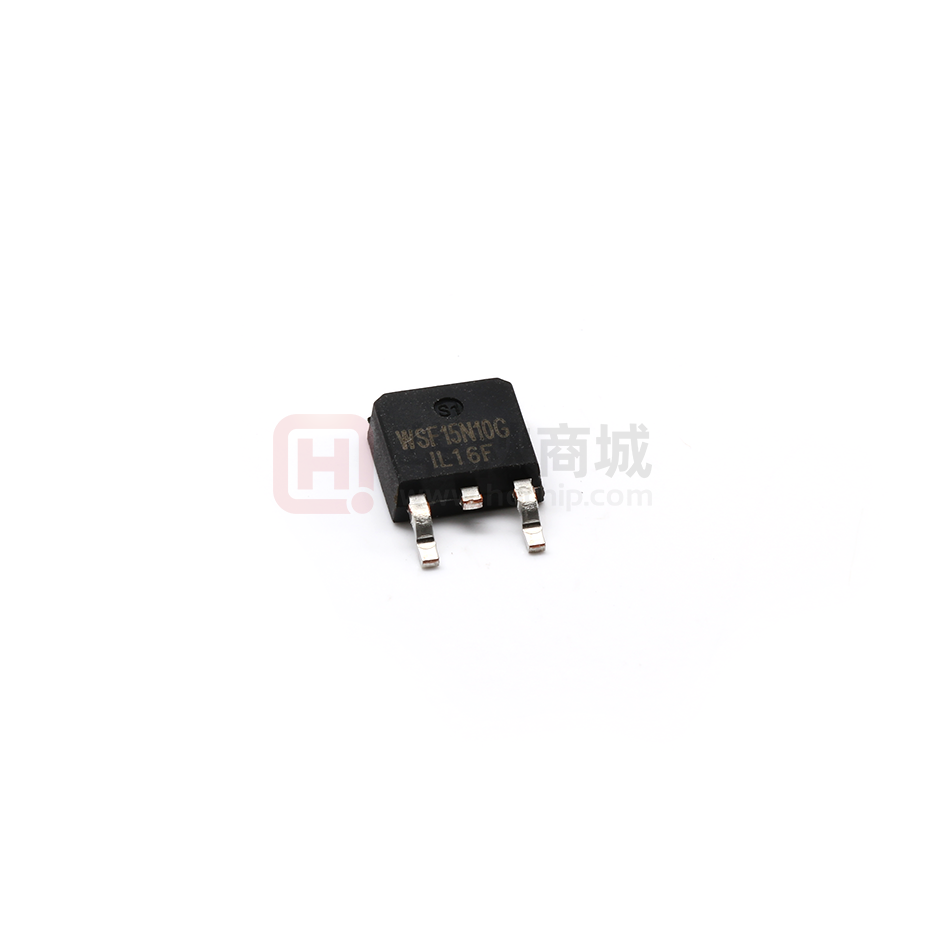
WSF15N10G
N-Ch MOSFET
Product Summery
General Description
The WSF15N10G uses advanced SGTMOS
technology to provide low RDS(ON), low gate
charge, fast switching and excellent avalanche
characteristics. This device is specially designed
to get better ruggedness and suitable to use in
Synchronous rectification applications
BVDSS
RDSON
ID
100V
75mΩ
15A
Applications
z Fast Switching
z DC-DC Power System
z Load Switch
Features
TO-252 Pin Configuration
z advanced SGTMOS technology
z Low gate charge
z Low RDS(ON)
Absolute Maximum Ratings at Tj=25℃ unless otherwise noted
Symbol
Parameter
Rating
Units
VDS
Drain-Source Voltage
100
V
VGS
Gate-Source Voltage
±20
V
15
A
45
A
5.5
mJ
36
W
ID
ID, pulse
EAS
Continuous Drain Current1)
2)
Pulsed Drain Current
4)
Single Pulse Avalanche Energy
3)
PD
Total Power Dissipation
TSTG
Storage Temperature Range
-55 to 150
℃
TJ
Operating Junction Temperature Range
-55 to 150
℃
Thermal Data
Symbol
Parameter
RθJA
Thermal Resistance Junction-ambient
RθJC
Thermal Resistance Junction-Case
www.winsok.tw
Page 1
5)
Typ.
Max.
Unit
---
62
℃/W
---
3.5
℃/W
Rev 2: Apr.2019
�WSF15N10G
N-Ch MOSFET
Electrical Characteristics (TJ=25 ℃, unless otherwise noted)
Symbol
BVDSS
Parameter
Drain-Source Breakdown Voltage
△BVDSS/△TJ BVDSS Temperature Coefficient
RDS(ON)
VGS(th)
Static Drain-Source On-Resistance2
Gate Threshold Voltage
Conditions
Min.
Typ.
Max.
Unit
100
---
---
V
Reference to 25℃ , ID=1mA
---
0.098
---
V/℃
VGS=10V , ID=5A
---
50
75
mΩ
VGS=4.5V , ID=2A
---
60
90
mΩ
VGS=VDS , ID =250uA
1.2
---
2.5
VGS=0V , ID=250uA
V
VDS=80V , VGS=0V , TJ=25℃
---
---
1
VDS=80V , VGS=0V , TJ=55℃
---
---
5
Gate-Source Leakage Current
VGS=±20V , VDS=0V
---
---
±100
nA
Rg
Gate Resistance
VDS=0V , VGS=0V , f=1MHz
---
28.8
---
Ω
Qg
Total Gate Charge (10V)
VGS=10 V ,
---
6.5
---
Qgs
Gate-Source Charge
VDS=50 V,
---
1.4
---
Qgd
Gate-Drain Charge
ID=5 A
---
1.4
---
Turn-On Delay Time
VGS=10 V,
---
14
---
Rise Time
VDS=50 V,
---
3.2
---
Turn-Off Delay Time
RG=2 Ω,
---
36
---
Fall Time
ID=5 A
---
14
---
Ciss
Input Capacitance
VGS=0 V,
---
310
---
Coss
Output Capacitance
VDS=25 V,
---
80
---
Crss
Reverse Transfer Capacitance
ƒ=100 KHz
---
50
---
Min.
Typ.
Max.
Unit
---
---
15
A
---
---
45
A
IDSS
Drain-Source Leakage Current
IGSS
Td(on)
Tr
Td(off)
Tf
uA
nC
ns
pF
Diode Characteristics
Symbol
IS
ISP
Parameter
Continuous diode current1)
Pulsed diode current2)
2)
Conditions
VG=VD=0V , Force Current
VSD
Diode Forward Voltage
VGS=0V , IS=5A , TJ=25℃
---
---
1.3
V
trr
Reverse Recovery Time
---
36
---
nS
Qrr
Reverse Recovery Charge
IF=5A ,
dI/dt=100A/µs , TJ=25℃
---
37
---
nC
1)
Calculated continuous current based on maximum allowable junction temperature.
2)
Repetitive rating; pulse width limited by max. junction temperature.
3)
Pd is based on max. junction temperature, using junction-case thermal resistance.
4)
VDD=50 V, RG=25 Ω, L=0.3 mH, starting Tj=25 °C.
5)
The value of RθJA is measured with the device mounted on 1 in 2 FR-4 board with 2oz. Copper, in a
still air environment with Ta=25 °C.
www.winsok.tw
Page 2
Rev 2: Apr.2019
�WSF15N10G
N-Ch MOSFET
Typical Characteristics
100
56
Tj = 25 ℃
10 V
VDS= 10 V
6V
Tj = 25 ℃
5.5 V
40
ID, Drain current(A)
ID, Drain current (A)
48
10
5V
32
4.5 V
24
4V
1
16
3.5 V
8
VGS= 3V
0.1
0
0
2
4
6
8
VDS, Drain-source voltage (V)
0
10
4
6
8
10
VGS, Gate-source voltage(V)
Figure 1, Typ. output characteristics
10
2
Figure 2, Typ. transfer characteristics
3
10.0
ID = 5 A
VDS = 50 V
VGS, Gate-source voltage(V)
Ciss
C, Capacitance (pF)
7.5
10
2
Coss
10
5.0
1
2.5
f =100 KHz
VGS = 0 V
10
Crss
0.0
0
0
20
40
60
80
0
100
1
VDS, Drain-source voltage (V)
BVDSS, Drain-source breakdown voltage (V)
5
6
7
100m
ID = 250 μA
ID = 5 A
RDS(ON), On-resistance(Ω)
VGS = 0 V
110
105
VGS = 10 V
75m
50m
25m
-50
0
50
100
-50
150
0
50
100
150
Tj, Junction Temperature (℃)
Tj, Junction temperature (℃)
Figure 5, Drain-source breakdown voltage
www.winsok.tw
4
Figure 4, Typ. gate charge
120
100
3
Qg, Gate charge(nC)
Figure 3, Typ. capacitances
115
2
Figure 6, Drain-source on-state resistance
Page 3
Rev 2: Apr.2019
�WSF15N10G
N-Ch MOSFET
100
ID = 250 μA
2.2
IS, Source current (A)
Vth, Threshold voltage (V)
2.4
2.0
Tj = 25 ℃
10
1.8
1.6
1
1.4
1.2
-50
0
50
100
0.1
150
0.0
0.4
Tj, Junction Temperature (℃)
Figure 7, Threshold voltage
2.0
15
4V
VGS=3.5 V
5V
4.5 V
5.5 V
ID, Drain current (A)
RDS(ON), On-resistance(Ω)
1.6
18
400m
10 V
200m
100m
12
9
6
3
0
8
16
24
32
40
48
0
56
0
20
40
ID, Drain current(A)
60
80
100
120
140
TC, Case Temperature (℃)
Figure 9, Drain-source on-state resistance
Figure 10, Drain current
10
10 μs
10
100 μs
1
1 ms
10 ms
RDS(ON) Limited
DC
0.1
0.01
0.01
0.1
1
10
100
zthjc Thermal Response(K/W)
100
ID, Drain current(A)
1.2
Figure 8, Forward characteristic of body diode
500m
300m
0.8
VSD, Source-Drain voltage (V)
D= tp/T
D= 1
0.5
1
0.1
0.05
0.1
0.01
10-5
www.winsok.tw
0.02
0.01
Single Pulse
10-4
10-3
10-2
10-1
100
tp Pulse width(s)
VDS, Drain-source voltage(V)
Figure 11, Safe operation area TC=25 ℃
0.2
Figure 12, Max. transient thermal impedance
Page 4
Rev 2: Apr.2019
�Attention�
1,�Any�and�all�Winsok�power�products�described�or�contained�herein�do�not�have�specifications�that�can�handle�
applications�that�require�extremely�high�levels�of�reliability,�such�as�lifeͲsupport�systems,�aircraft's�control�systems,�or�
other�applications�whose�failure�can�be�reasonably�expected�to�result�in�serious�physical�and/or�material�damage.� �
Consult�with�your�Winsok�power�representative�nearest�you�before�using�any�Winsok�power�products�described�or�
contained�herein�in�such�applications.�
2,Winsok�power�assumes�no�responsibility�for�equipment�failures�that�result�from�using�products�at�values�that�exceed,� �
even�momentarily,�rated�values�(such�as�maximum�ratings,�operating�condition�ranges,�or�other�parameters)�listed�in�
products�specifications�of�any�and�all�Winsok�power�products�described�or�contained�herein.�
3,�Specifications�of�any�and�all�Winsok�power�products�described�or�contained�herein�stipulate�the�performance,�
characteristics,�and�functions�of�the�described�products�in�the�independent�state,�and�are�not�guarantees�of�the�
performance,�characteristics,�and�functions�of�the�described�products�as�mounted�in�the�customer’s�products�or�
equipment.�To�verify�symptoms�and�states�that�cannot�be�evaluated�in�an�independent�device,�the�customer�should�always�
evaluate�and�test�devices�mounted�in�the�customer’s�products�or�equipment.�
4,�Winsok�power�Semiconductor�CO.,�LTD.�strives�to�supply�highͲquality�highͲreliability�products.�However,�any�and�all�
semiconductor�products�fail�with�some�probability.�It�is�possible�that�these�probabilistic�failures�could�give�rise�to�accidents�
or�events�that�could�endanger�human�lives�that�could�give�rise�to�smoke�or�fire,�or�that�could�cause�damage�to�other�
property.�When�designing�equipment,�adopt�safety�measures�so�that�these�kinds�of�accidents�or�events�cannot�occur.�Such�
measures�include�but�are�not�limited�to�protective�circuits�and�error�prevention�circuits�for�safe�design,�redundant�design,�
and�structural�design.�
5,In�the�event�that�any�or�all�Winsok�power�products(including�technical�data,�services)�described�or�contained�herein�are�
controlled�under�any�of�applicable�local�export�control�laws�and�regulations,�such�products�must�not�be�exported�without�
obtaining�the�export�license�from�the�authorities�concerned�in�accordance�with�the�above�law.�
6,�No�part�of�this�publication�may�be�reproduced�or�transmitted�in�any�form�or�by�any�means,�electronic�or�mechanical,�
including�photocopying�and�recording,�or�any�information�storage�or�retrieval�system,�or�otherwise,�without�the�prior�
written�permission�of�Winsok�power�Semiconductor�CO.,�LTD.�
7,�Information�(including�circuit�diagrams�and�circuit�parameters)�herein�is�for�example�only;�it�is�not�guaranteed�for�
volume�production. Winsok�power�believes�information�herein�is�accurate�and�reliable,�but�no�guarantees�are�made�or�
implied�regarding�its�use�or�any�infringements�of�intellectual�property�rights�or�other�rights�of�third�parties.�
8,�Any�and�all�information�described�or�contained�herein�are�subject�to�change�without�notice�due�to�product/technology�
improvement,etc.�When�designing�equipment,�refer�to�the�"Delivery�Specification"�for�the�Winsok�power�product�that�you� �
Intend�to�use.�
9,�this�catalog�provides�information�as�of�Sep.2014. Specifications�and�information�herein�are�subject�to�change�without�
notice.�
�


 工商网监
湘ICP备2023018690号
工商网监
湘ICP备2023018690号
