ZL40120
Low Power, Current Feedback
Quad Operational Amplifier
Data Sheet
Features
•
•
•
•
•
April 2003
280MHz small signal bandwidth
1100V/µs slew rate
3.3mA/channel static supply current
60Mhz gain flatness to +/- 0.1dB
14 pin SOIC
Ordering Information
ZL40120/DCA
ZL40120/DCB
-40°C to +85°C
Applications
•
•
•
•
•
(tubes) 14 lead SOIC
(tape and reel) 14 lead SOIC
The 280MHz Av=+1V/V small signal bandwidth and
1100V/µs slew rate make the device an excellent
solution for component video applications such as
driving RGB signals down significant cable lengths.
Video switchers/routers
Video line drivers
Twisted pair driver/receiver
Active filters
Cable drivers
Other applications which may take advantage of the
ZL40120 dynamic performance features and matched
amplifiers include low cost high order active filters and
twisted pair driver/receivers.
Description
The ZL40120 is a low power, quad, current feedback
operational amplifier offering high performance at a low
cost. The device provides a very high output current
drive capability of 65mA while requiring only 3.3mA of
static supply current per channel. This feature makes
the ZL40120 the ideal choice where a high density of
high speed devices is required.
Out_1
14 Out_4
1
13 In_n_4
In_n_1 2
1
4
12 In_p_4
In_p_1 3
ZL40120
V+ 4
11 V10 In_p_3
In_p_2 5
2
3
In_n_2 6
9 In_n_3
Out_2 7
8 Out_3
Figure 1 - Functional Block Diagram and Pin Connection
1
�ZL40120
Data Sheet
Application Notes
Current Feedback Op Amps
Current feedback op amps offer several advantages over voltage feedback amplifiers:
•
•
•
AC bandwidth not dependent on closed loop gain
High Slew Rate
Fast settling time
The architecture of the current feedback opamp consists of a high impedance non-inverting input and a low
impedance inverting input which is always feedback connected. The error current is amplified by a transimpedance
amplifier which can be considered to have gain
Z( f ) =
Zo
f
1 + j
fo
where Zo is the DC gain.
It can be shown that the closed loop non-inverting gain is given by
Vout
=
Vin
Av
fR f
1 + j
fo Zo
where Av is the DC closed loop gain, Rf is the feedback resistor. The closed loop bandwidth is therefore given by
BWCL =
f o Z o GBOL
=
Rf
Rf
and for low values of closed loop gain Av depends only on the feedback resistor Rf and not the closed loop gain.
This can readily be seen from the performance characteristic frequency response graph with varying Rf
It can be shown that increasing the value of Rf
•
•
•
•
•
Increases closed loop stability
Decreases loop gain
Decreases bandwidth
Reduces gain peaking
Reduces overshoot
Using a resistor value of Rf=510Ω for Av=+2 V/V gives good stability and bandwidth. However since requirements
for stability and bandwidth vary it may be worth some experimentation to find the optimal Rf for a given application.
Layout Considerations
Correct high frequency operation requires a considered PCB layout as stray capacitances have a strong influence
over high frequency operation for this device. This is particularly important for high performance current feedback
opamps. The Zarlink evaluation board serves as a good example layout that should be copied. The following
guidelines should be followed:
•
•
•
Include 6.8uF tantalum and 0.1uF ceramic capacitors on both positive and negative supplies
Remove the ground plane under and around the part, especially near the input and output pins to reduce
parasitic capacitances
Minimize all trace lengths to reduce series inductance
2
Zarlink Semiconductor Inc.
�ZL40120
Data Sheet
Application Diagrams
Vcc
6.8uF
•
•
•
0.1uF
Vin
•
Vout
•
¼ ZL40120
Rf
Rin
•
Ra
•
0.1uF
Vout
Rf
= Av = 1 +
Vin
Ra
•
•
6.8uF
Vee
Figure 2 - Non-inverting Gain
Vcc
6.8uF
•
•
•
Rb
0.1uF
Vin
Vout
•
¼ ZL40120
Rf
•
•
Ra
Rin
•
0.1uF
•
•
Vout
Rf
= Av = −
Vin
Ra
6.8uF
Vee
Figure 3 - Inverting Gain
Zarlink Semiconductor Inc.
3
�ZL40120
Data Sheet
Absolute Maximum Ratings
Parameter
Symbol
Min
Max
Units
VIN
±1.2
V
1
Vin Differential
2
Output Short Circuit Protection
VOS/C
See Apps
Note in this
data sheet
3
Supply voltage
V+, V-
±6.5
V
4
Voltage at Input Pins
5
Voltage at Output Pins
6
EDS Protection
(HBM Human Body Model)
(see Note 2)
7
Storage Temperature
8
9
Note 1:
V(+IN), V(-IN)
V-
V+
V
VO
V-
V+
V
2
(see Note 3)
kV
-55
+150
°C
Latch-up test
±100mA
for 100ms
(see Note 4)
Supply transient test
20% pulse
for 100ms
(see Note 5)
Absolute Maximum Ratings indicate limits beyond which damage to the device may occur. Operating Ratings indicate
conditions for which the device is intended to be functional, but specific performance is not guaranteed. For guaranteed
specifications and the test conditions, see the Electrical Characteristics.
Note 2:
Human body model, 1.5k Ω in series with 100pF. Machine model, 20 Ω in series with 100pF.
Note 3:
0.8kV between the pairs of +INA, -INA and +INB pins only. 2kV between supply pins, OUTA or OUTB pins and any input pin.
Note 4:
±100mA applied to input and output pins to force the device to go into "latch-up". The device passes this test to JEDEC spec
17.
Note 5:
Positive and Negative supply transient testing increases the supplies by 20% for 100ms.
Operating Range
Characteristic
4
Min
Typ
Max
Units
Supply Voltage (Vcc)
±4.0
±6.0
V
Operating Temperature (Ambient)
-40
+85
°C
Junction to Ambient resistance
Rth(j-a)
150
°C
4 layer
FR4 board
Junction to Case resistance
Rth(j-c)
60
°C
4 layer
FR4 board
Zarlink Semiconductor Inc.
Comments
�ZL40120
Data Sheet
Electrical Characteristics - Vcc=±5V, Tamb=25C(typ.),Tamb=-40C to +85C(min-max), Av=+2V/V,
Rf=510Ω, Rload=100Ω unless specified.
Typ
25C
Min/
Max
25C
Min/
Max
–40 to
+85C
Av=+1; Vo < 0.5Vp-p;
Rf=1.1kΩ
280
-
-
MHz
C
Av=+2; Vo < 0.5Vp-p;
Rf=510Ω
230
-
-
MHz
C
Av=+2; Vo < 5Vp-p;
Rf=510Ω
130
-
-
MHz
C
+/- 0.1dB Flatness
Av=+2; Vo < 0.5Vp-p;
Rf=510Ω
60
-
-
MHz
C
Differential Gain (NTSC)
Rload=150Ω
0.02
-
-
%
C
Differential Phase (NTSC)
Rload=150Ω
0.06
-
-
deg.
C
Vout=0.5V Step
1.4
-
-
ns
C
Vout=5V Step
3.6
-
-
ns
C
Settling Time to 0.1%
Vout=2V Step
6
-
-
ns
C
Overshoot
Vout=0.5V Step
6
-
-
%
C
Slew Rate
Vout=5V Step
1100
-
-
V/µs
C
Characteristic
Conditions
Units
Test
Type1
Frequency Domain Response
-3dB Bandwidth
Time Domain Response
Rise and Fall Time
Noise and Distortion
2nd Harmonic Distortion
Vout=2Vp-p, 1MHz
-78
-
-
dBc
C
3nd Harmonic Distortion
Vout=2Vp-p, 1MHz
-88
-
-
dBc
C
Voltage
>1MHz
6.4
-
-
nV Hz
C
Non-Inverting Current
>1MHz
1.0
-
-
pV Hz
C
Inverting Current
>1MHz
9.3
-
-
pA Hz
C
Input Offset Voltage
1.4
± 6.0
± 7.5
Average Drift
-
-
15
1.3
±2.6
-
-
Equivalent Input Noise
Static, DC Performance
Input Bias Current – Non-inverting
Average Drift
Zarlink Semiconductor Inc.
mV
A
uV/deg. C
C
±2.8
uA
A
2.6
nA/deg. C
C
5
�ZL40120
Data Sheet
Characteristic
Conditions
Input Bias Current – Inverting
Average Drift
Typ
25C
Min/
Max
25C
Min/
Max
–40 to
+85C
4.4
±14
±15
uA
A
-
-
15
nA/deg. C
C
Units
Test
Type1
Power Supply Rejection Ratio (+ve)
DC
65
63
62
dB
A
Power Supply Rejection Ratio (-ve)
DC
62
58
56
dB
A
Common Mode Rejection Ratio
DC
57
54
53
dB
A
Supply Current (per Channel)
Quiescent
3.3
4.5
4.7
mA
A
Input Resistance (Non-inverting)
19.0
-
-
MΩ
C
Input Capacitance (Non-inverting)
1
-
-
pF
C
±2.3
±2.2
±1.9
V
A
±2.8
±2.7
±2.6
V
A
65
-
-
mA
C
110
-
-
mΩ
C
Miscellaneous Performance
Common Mode Input Range
Output Voltage Range
Rload=100Ω
Output Current (max)
Output Resistance, Closed Loop
DC
NOTE 1: Test Types:
(A) 100% tested at 25°C. Over temperature limits are set by characterization and simulation.
(B) Limits set by characterization or simulation.
(C) Typical value only for information.
6
Zarlink Semiconductor Inc.
�ZL40120
Data Sheet
Typical Performance Characteristics - Tamb=25degC, Vsupply=± 5V, Rload=100Ω, Av=+2V/V,
Rf=510Ω, unless otherwise specified.
Non-Inverting Frequency Response
2
200
Av =+2
Rf = 510
Normalised Gain (dB)
-2
Av =+1
Rf = 1.1k
Av =+8
Rf = 200
-4
150
100
50
Phase
-6
0
-8
-50
Av =+4
Rf = 150
-10
-12
-100
-150
Vo = 0.5Vp-p
-14
1
Phase (deg.)
Gain
0
10
100
-200
1000
Frequency (MHz)
Zarlink Semiconductor Inc.
7
�ZL40120
Data Sheet
Non-Inverting Frequency Response varying Rf
2
Rf=390
0
Normalised Gain (dB)
-2
Rf=250
Rf=700
-4
Rf=510
-6
-8
-10
-12
-14
Vo=0.5Vp-p
-16
-18
10
100
1000
Frequency (MHz)
Frequency Response for Varying Rload
2
0
RL = 1k
RL = 100
Gain (dB)
-2
-4
RL = 25
-6
Vo = 0.5V p-p
-8
-10
10
100
Frequency (MHz)
8
Zarlink Semiconductor Inc.
1000
�ZL40120
Data Sheet
Large Signal Gain
0
-2
Vo = 2V p-p
Gain (dB)
-4
Vo = 1V p-p
Vo = 5V p-p
-6
-8
Vo = 4V p-p
-10
-12
-14
-16
10
100
1000
Frequency (MHz)
Open Loop Transimpedance Gain and Phase
120
0
-30
Transimpedance Gain
100
90
-60
Transimpedance Phase
-90
80
-120
70
-150
60
-180
50
-210
40
1.0E+03
1.0E+04
1.0E+05
1.0E+06
1.0E+07
1.0E+08
Transimpedance Phase
Transimpedance Gain
110
-240
1.0E+09
Frequency (Hz)
Zarlink Semiconductor Inc.
9
�ZL40120
Data Sheet
Harmonic Distortion vs Frequency
-40
Vo = 2V p-p
2nd & 3rd Harmonic Distortion (dBc)
-50
-60
2nd Harmonic
-70
-80
-90
3rd Harmonic
-100
1
10
100
Frequency (MHz)
CMRR
70
T = - 40 degC
Rejection Ration (dB)
60
50
T = + 25 degC
T = + 85 degC
40
30
20
10
0
1.0E+03
1.0E+04
1.0E+05
1.0E+06
Frequency (Hz)
10
Zarlink Semiconductor Inc.
1.0E+07
1.0E+08
�ZL40120
Data Sheet
PSRR +ve
80
T = - 40 degC
Rejection Ration (dB)
70
60
T = + 25 degC
50
T = + 85 degC
40
30
20
10
0
1.0E+03
1.0E+04
1.0E+05
1.0E+06
1.0E+07
1.0E+08
Frequency (Hz)
PSRR -ve
70
T = - 40 degC
Rejection Ration (dB)
60
50
T = + 25 degC
T = + 85 degC
40
30
20
10
0
1.0E+03
1.0E+04
1.0E+05
1.0E+06
1.0E+07
1.0E+08
Frequency (Hz)
T
Zarlink Semiconductor Inc.
11
�ZL40120
Data Sheet
Input Voltage and Current Noise
Current Noise (pA/SQRT(Hz)
Voltage Noise (nV/SQRT(Hz)
100
Inverting Input Current Noise
10
Input Voltage Noise
1
Non-Inverting Input Current
0.1
1.0E+01
1.0E+02
1.0E+03
1.0E+04
1.0E+05
1.0E+06
1.0E+07
Frequency (Hz)
Supply Current vs Temperature
3.55
3.50
Supply Current (mA)
3.45
3.40
3.35
3.30
3.25
3.20
3.15
3.10
3.05
3.00
-40
-20
0
20
40
60
Die Temp (deg. C)
12
Zarlink Semiconductor Inc.
80
100
120
140
�ZL40120
Data Sheet
DC Drift Over Temperature
5.00
4.00
3.50
Input Bias Inv
3.00
2.50
Input Offset Voltage
2.00
1.50
1.00
Input Bias Non-Inv
0.50
0.00
-40
-20
0
20
40
60
80
100
120
140
Die Temp (deg. C)
Large and Small Signal Pulse Response
3
0.6
Vout = 5V Step
0.4
1
0.2
Vout = 0.5V Step
0
0
-1
-0.2
-2
-0.4
-3
Small Signal Vout (V)
2
Large Signal Vout (V)
Input Offset Voltage (mV)
Input Bias Current (uA)
4.50
-0.6
0
10
20
30
40
50
60
70
80
Time (ns)
Zarlink Semiconductor Inc.
13
�ZL40120
Data Sheet
Closed Loop Output Impedance
Closed Loop Output Impedance (Ohms)
10
1
0.1
0.01
0.01
0.1
1
10
100
Frequency (MHz)
Differential Gain & Phase ZL40120 / ZL40121
NTSC
RL=150?
Best fit Gain
Best fit Phase
0.07
0.06
0.05
Differential Gain & Phase (?% & ?°)
0.04
0.03
0.02
0.01
0
-0.01
-0.02
-0.03
-0.04
-0.05
-0.06
-0.07
-0.7
-0.6
-0.5
-0.4
-0.3
-0.2
-0.1
0
0.1
bias voltage
14
Zarlink Semiconductor Inc.
0.2
0.3
0.4
0.5
0.6
0.7
�Package Code
c Zarlink Semiconductor 2003 All rights reserved.
ISSUE
ACN
DATE
APPRD.
Previous package codes
�For more information about all Zarlink products
visit our Web Site at
www.zarlink.com
Information relating to products and services furnished herein by Zarlink Semiconductor Inc. or its subsidiaries (collectively “Zarlink”) is believed to be reliable.
However, Zarlink assumes no liability for errors that may appear in this publication, or for liability otherwise arising from the application or use of any such
information, product or service or for any infringement of patents or other intellectual property rights owned by third parties which may result from such application or
use. Neither the supply of such information or purchase of product or service conveys any license, either express or implied, under patents or other intellectual
property rights owned by Zarlink or licensed from third parties by Zarlink, whatsoever. Purchasers of products are also hereby notified that the use of product in
certain ways or in combination with Zarlink, or non-Zarlink furnished goods or services may infringe patents or other intellectual property rights owned by Zarlink.
This publication is issued to provide information only and (unless agreed by Zarlink in writing) may not be used, applied or reproduced for any purpose nor form part
of any order or contract nor to be regarded as a representation relating to the products or services concerned. The products, their specifications, services and other
information appearing in this publication are subject to change by Zarlink without notice. No warranty or guarantee express or implied is made regarding the
capability, performance or suitability of any product or service. Information concerning possible methods of use is provided as a guide only and does not constitute
any guarantee that such methods of use will be satisfactory in a specific piece of equipment. It is the user’s responsibility to fully determine the performance and
suitability of any equipment using such information and to ensure that any publication or data used is up to date and has not been superseded. Manufacturing does
not necessarily include testing of all functions or parameters. These products are not suitable for use in any medical products whose failure to perform may result in
significant injury or death to the user. All products and materials are sold and services provided subject to Zarlink’s conditions of sale which are available on request.
Purchase of Zarlink’s I2C components conveys a licence under the Philips I2C Patent rights to use these components in and I2C System, provided that the system
conforms to the I2C Standard Specification as defined by Philips.
Zarlink, ZL and the Zarlink Semiconductor logo are trademarks of Zarlink Semiconductor Inc.
Copyright Zarlink Semiconductor Inc. All Rights Reserved.
TECHNICAL DOCUMENTATION - NOT FOR RESALE
�
很抱歉,暂时无法提供与“ZL40120/DCB”相匹配的价格&库存,您可以联系我们找货
免费人工找货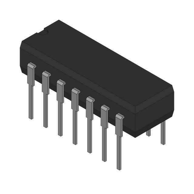


 工商网监
湘ICP备2023018690号
工商网监
湘ICP备2023018690号
