IQS227AS-00000000-TSR 数据手册
Azoteq
IQ Switch®
ProxSense® Series
IQS227AS/B DATASHEET
Single channel capacitive proximity
and touch controller
The IQS227AS/B ProxSense® IC is a fully integrated Self Capacitive sensor with dual outputs (Touch
and Proximity outputs).
Features
>
>
>
>
>
>
>
>
Sub 2.5µA in Low Power Mode while sensing Proximity
Automatic Tuning Implementation (ATI) - Automatic tuning of sense electrode
Internal Capacitor Implementation (ICI) – reference capacitor on-chip
Supply voltage: 1.8V to 3.6V
Minimum external components
Data streaming option
RoHS2
Advanced on-chip digital signal processing
Compliant
User selectable (OTP): 4 Power Modes
IO sink / source
Time-out for stuck key
Output mode (Direct / Latch / Toggle)
Proximity and Touch Button sensitivity
Applications
>
>
>
>
>
>
>
>
>
>
>
>
LCD, Plasma & LED TVs
GSM cellular telephones – On ear detection / touch keys
LED flashlights or headlamps
White goods and appliances
Office equipment, toys, sanitary ware
Flame proof, hazardous environment Human Interface Devices
Proximity detection enables backlighting activation
Wake-up from standby applications
Replacement for electromechanical switches
Find-In-The-Dark (FITD) applications
Automotive: Door pocket lighting, electric window control
GUI trigger on Proximity detected.
Available options
TA
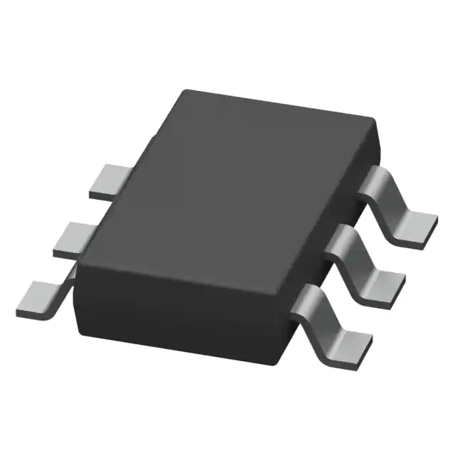
TSOT23-6
WLCSP-8
DFN-6
-20°C to 85°C
IQS227AS
-
-
-40°C to 85°C
IQS227B
IQS227B
IQS227B
Copyright © Azoteq (Pty) Ltd 2021
All rights reserved
IQS227AS/B Datasheet
Revision 1.40
Page 1 of 37
October 2021
�IQ Switch®
ProxSense® Series
Azoteq
Contents
IQS227AS/B DATASHEET................................................................................................................................ 1
1 OVERVIEW ..................................................................................................................................................... 5
1.1 APPLICABILITY ............................................................................................................................................ 5
1.2 ANALOGUE FUNCTIONALITY ......................................................................................................................... 5
2 PACKAGING AND PIN-OUT .......................................................................................................................... 6
2.1 IQS227AS/B.............................................................................................................................................. 6
2.1.1 TSOT23-6 Pin-out ............................................................................................................................. 6
2.1.2 WLCSP-8 Pin-out .............................................................................................................................. 7
2.1.3 DFN-6 Pin-out ................................................................................................................................... 8
2.2 SCHEMATIC................................................................................................................................................. 9
2.2.1 TSOT23-6 .......................................................................................................................................... 9
2.2.2 WLCSP-8........................................................................................................................................... 9
2.2.3 DFN-6 .............................................................................................................................................. 10
3 USER CONFIGURABLE OPTIONS ............................................................................................................. 11
3.1 CONFIGURING OF DEVICES ........................................................................................................................ 11
4 MEASURING CAPACITANCE USING THE CHARGE TRANSFER METHOD .......................................... 14
5 DESCRIPTIONS OF USER OPTIONS ......................................................................................................... 14
5.1 PROXIMITY / TOUCH SENSOR ..................................................................................................................... 15
5.2 LOGIC SELECT FOR OUTPUTS ..................................................................................................................... 15
5.3 OUTPUT PIN FUNCTION .............................................................................................................................. 15
5.3.1 Output function: Active .................................................................................................................... 15
5.3.2 Output function: Latch (for tLATCH) .................................................................................................... 15
5.3.3 Output function: Toggle ................................................................................................................... 16
5.4 PROXIMITY THRESHOLD ............................................................................................................................ 16
5.5 TOUCH THRESHOLD .................................................................................................................................. 16
5.6 POWER MODES......................................................................................................................................... 17
5.7 BASE VALUES ........................................................................................................................................... 18
5.8 MULTIPLIERS ............................................................................................................................................ 18
5.9 CHARGE TRANSFER .................................................................................................................................. 18
5.10 ATI TARGET COUNTS .............................................................................................................................. 18
5.11 NOISE DETECT ........................................................................................................................................ 18
5.12 ENABLE PARTIAL ATI .............................................................................................................................. 18
5.13 FILTERS USED BY THE IQS227AS/B ........................................................................................................ 18
5.13.1 Long Term Average (LTA) ............................................................................................................ 18
5.13.2 IIR Raw Data filter ......................................................................................................................... 19
6 DATA STREAMING MODE .......................................................................................................................... 19
6.1 EVENT MODE ............................................................................................................................................ 21
6.2 I2C ........................................................................................................................................................... 21
7 AUTO TUNING IMPLEMENTATION (ATI)................................................................................................... 21
7.1 AUTOMATIC ATI ........................................................................................................................................ 21
7.2 IQS227AS/B NOISE IMMUNITY .................................................................................................................. 22
8 ELECTRICAL SPECIFICATIONS ................................................................................................................ 23
8.1 ABSOLUTE MAXIMUM SPECIFICATIONS ....................................................................................................... 23
8.2 GENERAL CHARACTERISTICS ..................................................................................................................... 23
Copyright © Azoteq (Pty) Ltd 2021
All rights reserved
IQS227AS/B Datasheet
Revision 1.40
Page 2 of 37
October 2021
�IQ Switch®
ProxSense® Series
Azoteq
8.3 OUTPUT CHARACTERISTICS ....................................................................................................................... 24
8.4 PACKAGING INFORMATION ......................................................................................................................... 25
8.4.1 TSOT23-6 ........................................................................................................................................ 25
8.4.2 WLCSP-8......................................................................................................................................... 26
8.4.3 DFN-6 .............................................................................................................................................. 27
8.5 PACKAGE MSL ......................................................................................................................................... 28
9 DATASHEET AND PART-NUMBER INFORMATION ................................................................................. 29
9.1 ORDERING INFORMATION........................................................................................................................... 29
9.2 DEVICE MARKING – TOP ............................................................................................................................ 30
9.2.1 TSOT23-6 Packaging Markings ...................................................................................................... 30
9.2.2 WLCSP-8 Package Markings .......................................................................................................... 31
9.2.3 DFN-6 Package Markings ............................................................................................................... 31
9.3 DEVICE MARKING - BOTTOM ...................................................................................................................... 31
9.4 TAPE & REEL SPECIFICATION .................................................................................................................... 32
APPENDIX A. MEMORY MAP ........................................................................................................................ 33
APPENDIX B. CONTACT INFORMATION ..................................................................................................... 37
Copyright © Azoteq (Pty) Ltd 2021
All rights reserved
IQS227AS/B Datasheet
Revision 1.40
Page 3 of 37
October 2021
�IQ Switch®
ProxSense® Series
Azoteq
List of Abbreviations
ATI
Automatic Tuning Implementation
BP
Boost Power Mode
CS
Counts (Number of Charge Transfers)
Cs
Internal Reference Capacitor
EMI
Electromagnetic Interference
ESD
Electro-Static Discharge
FTB/EFT
(Electrical) Fast Transient Bursts
GND
Ground
HC
Halt Charge
LP
Low Power Mode
LTA
Long Term Average
ND
Noise Detect
THR
Threshold
Copyright © Azoteq (Pty) Ltd 2021
All rights reserved
IQS227AS/B Datasheet
Revision 1.40
Page 4 of 37
October 2021
�IQ Switch®
ProxSense® Series
Azoteq
1 Overview
The IQS227AS/B is a single channel
capacitive proximity and touch controller with
an internal voltage regular and reference
capacitor (Cs).
The IQS227AS/B devices have dedicated
pin(s) for the connection of sense electrodes
(Cx) and output pins for proximity events on
POUT and touch event on TOUT. The output
pins can be configured for various output
methods including a serial data streaming
option on TOUT (1-wire protocol) or debug I2C.
Device configuration is determined by one
time programmable (OTP) options.
The devices automatically track slow varying
environmental changes via various filters,
detect noise and has an Automatic Tuning
Implementation (ATI) to tune the device sense
electrode(s). The IQS227AS/B is built on
ProxSense® new low voltage platform ideal for
battery application (down to 1.8V).
1.1 Applicability
All specifications, except where specifically
mentioned otherwise, provided by this
datasheet are applicable to the following
ranges:
>
Temperature:
• IQS227AS:
-20°C to +85°C
• IQS227B:
-40°C to +85°C
> Supply voltage (VDDHI): 1.8V to 3.6V
1.2 Analogue Functionality
The analogue circuitry measures the
capacitance of a sense electrode attached to
the Cx pin through a charge transfer process
that is periodically initiated by the digital
circuitry. The measuring process is referred to
a conversion and consists of the discharging
of reference capacitor and Cx, the charging of
Cx and then a series of charge transfers from
Cx to Cs until a trip voltage is reached. The
number of charge transfers required to reach
the trip voltage is referred to as the Counts
(CS).
Copyright © Azoteq (Pty) Ltd 2021
All rights reserved
The capacitance measurement circuitry
makes use of an internal C s and voltage
reference (VREF).
The analogue circuitry
functionality for:
further
provides
> Power on reset (POR) detection.
> Reset detection.
> Detection of a watch dog timer (WDT)
IQS227AS/B Datasheet
Revision 1.40
Page 5 of 37
October 2021
�Azoteq
IQ Switch®
ProxSense® Series
2 Packaging and Pin-out
2.1 IQS227AS/B
The IQS227AS is available in a TSOT23-6 package, the IQS227B is available in TSOT23-6 or
WLCSP-8 package
2.1.1 TSOT23-6 Pin-out
TOUT 1
227AS/B
6 Cx
GND 2
5 VDDHI
POUT 3
4 VREG
Figure 2.1: Pin-out of IQS227AS/B in TSOT23-6 package.
22-Bxx
Table 2.1:Pin-out description.
IC NAME
Batch code
IQS227AS/B
227Bxx
Pin
Name
Type
Function
1
TOUT
2
GND
Ground
GND Reference
3
POUT
Digital Out
Proximity Output
4
VREG
Analogue Output
5
VDDHI
Supply Input
6
CX
IC Digital
NAME
Out
Batch
Touch Output
227Axx
code
Internal Regulator Pin
Supply Voltage Input
ICAnalogue
NAMEI/O
Sense Electrode
Batch
code
22-Axx
IC NAME
Copyright © Azoteq (Pty) Ltd 2021
All rights reserved
IQS227AS/B Datasheet
Revision 1.40
Batch code
Page 6 of 37
October 2021
�Azoteq
IQ Switch®
ProxSense® Series
2.1.2 WLCSP-8 Pin-out
1
2
3
4
IQS227
8
7
6
5
Figure 2.2 IQS227B 8-pin WLCSP
Table 2.2 8 -pin WLCSP Pin-out Description
IQS227B 8-pin WLCSP
Pin
Name
Type
Function
1
Cx
Sense electrode
Connect to conductive area intended for sensor
2
TOUT
Digital Out
Touch Output
3
VREG
Regulator output
Requires external capacitor
4
VSS
Signal GND
5
INPUT
Digital Input
Floating input during runtime.
Recommended: Connect to POUT
6
POUT
Digital Out
Proximity Output
7
VDDHI
Supply Input
Supply Voltage Input
Configuration pin
Connection for OTP programming. Floating input during
runtime.
Recommended: Connect to TOUT pin. Programming
can still be performed using this pin, provided a diode is
used. (See AZD026 – Configuration Tools Overview)
8
PGM
Copyright © Azoteq (Pty) Ltd 2021
All rights reserved
IQS227AS/B Datasheet
Revision 1.40
Page 7 of 37
October 2021
�Azoteq
IQ Switch®
ProxSense® Series
2.1.3 DFN-6 Pin-out
POUT 3
TOUT 1
5
GND 2
4
POUT 3
6
Cx
TOUT 1
5
VDDHI
GND 2
4
VREG
POUT 3
IQS228
GND 2
6
IQS227
IQS211
TOUT 1
Figure 2.3: Pin-out of IQS227B in DFN-6 package.
Table 2.3:Pin-out description.
22-Bxx
IQS227B 6-pin DFN
Pin
Name
IC
NAME
1
TOUT
2
GND
3
POUT
4
ICVREG
NAME
Type
227Bxx
Ground
Digital Out
Digital Out
Analogue Output
Function
Batch code
Touch Output
GND Reference
Proximity Output
Batch
code
Internal
Regulator Pin
5
VDDHI
Supply Input
Supply Voltage Input
6
CX
Analogue I/O
Sense Electrode
227Dxx
IC NAME
Batch code
22-Dxx
IC NAME
Copyright © Azoteq (Pty) Ltd 2021
All rights reserved
Batch code
IQS227AS/B Datasheet
Revision 1.40
Page 8 of 37
October 2021
6
5
4
�IQ Switch®
ProxSense® Series
Azoteq
2.2 Schematic
2.2.1 TSOT23-6
Refer to AZD008 for
touch key designs
Figure 2.4: Typical application schematic of IQS227AS/B. 100pF capacitors are optional for added RF immunity. Place
all decoupling capacitors (on VDDHI and VREG) as close to the IC as possible.
Where a system level ESD strike is found to cause the IC to go into ESD induced latch-up, it is
suggested that the supply current to the IQS227 IC is limited by means of a series resistor that could
limit the maximum supply current to the IC to
>
This section describes the individual user
programmable options of the IQS227AS/B in
more detail.
>
User programmable options are programmed to
One Time Programmable (OTP) fuse registers
(refer to Section 3).
HIGH=Logical ‘1’ and LOW=Logical ‘0’.
The following sections are explained with
POUT and TOUT taken as ‘Active LOW’.
The default is always where bits are set to
0.
Refer to section 0 for the sourcing and sinking
capabilities POUT and TOUT. These pins are
sourced from VDDHI and will be turned HIGH
(when active high) for a minimum time of t HIGH,
and LOW for a minimum time of tLOW (when
active low).
Note:
Copyright © Azoteq (Pty) Ltd 2021
All rights reserved
IQS227AS/B Datasheet
Revision 1.40
Page 14 of 37
October 2021
�IQ Switch®
ProxSense® Series
Azoteq
5.1 Proximity / Touch Sensor
Configuration: Bank0 bit5
The IQS227AS/B provides a Proximity output
on POUT and a Touch output on TOUT, and
does not need to be configured.
LOGIC: Output logic select Bit
Selection
0
Active Low
1
Active High
5.2 Logic select for outputs
5.3 Output pin function
The logic used by the device can be selected as
active HIGH or active LOW. The output pins,
POUT and TOUT, will function based on this
selection. The I/O’s are push pull in both
directions and does not require a pull-up
resistor. When configured as Active High, the
I/O’s will remain high at POR until ATI has been
completed. ATI times will vary based on the
capacitive load on the sensor, but typically do
not exceed 500ms.
Various options for the function of the output
pin(s) are available. These are selected as
follow:
Configuration: Bank0 bit7-6
FUNC1:FUNC0 OUTPUT Pins’ functions
Bit
Selection
00
POUT active, TOUT active
01
POUT latch, TOUT active
10
POUT active, TOUT toggle
11
POUT latch, TOUT toggle
5.3.1 Output function: Active
With a Proximity or Touch event, the output pin
will change to LOW and stay LOW for as long
as the event remains (see Figure 5.1 Also refer
to the use of tHALT section 5.13.1 that may cause
the termination of the event.
User Actuation
1
0
Output Pin
1
0
Figure 5.1: Active Mode Output Configuration
5.3.2 Output function: Latch (for tLATCH)
With a Proximity or Touch event, the output pin
will latch LOW for tLATCH seconds (4 seconds).
When the event terminates prior to tLATCH the
output pin will remain LOW.
Copyright © Azoteq (Pty) Ltd 2021
All rights reserved
When the event remains active longer than
tLATCH the output pin will remain LOW as long as
the event remains active (see Figure 5.2)
When a subsequent event is made before the
latch time (4 seconds) has passed, the timer will
reset and the output will remain low for another
duration of tLATCH seconds (4 seconds). For
more details see Figure 5.2.
IQS227AS/B Datasheet
Revision 1.40
Page 15 of 37
October 2021
�Azoteq
IQ Switch®
ProxSense® Series
User Actuation
1
0
tLATCH
tLATCH
Output Pin
tLATCH
+ time that User Actuation stays active
1
0
Figure 5.2: Latch Mode Output Configuration
5.3.3 Output function: Toggle
The output pin will toggle with every Proximity
or Touch event occurring. Thus when an event
occurs and the output is LOW the output will
become HIGH and when the output is HIGH the
output will become LOW (see Figure 5.3)
User Actuation
1
0
Output Pin
1
0
Figure 5.3: Toggle Mode Output Configuration
Configuration: Bank0 bit1-0
5.4 Proximity Threshold
The IQS227AS/B has 4 proximity threshold
settings. The proximity threshold is selected by
the designer to obtain the desired sensitivity and
noise immunity. The proximity event is triggered
based on the selected proximity threshold; the
Counts (CS) and the LTA (Long Term Average).
The threshold is expressed in terms of counts;
the same as CS (refer to 0)
PTHR =< LTA-CS
Where LTA is the Long Term Average (refer to
PTHR1:PTHR0 Proximity Thresholds
Bit
Selection
00
4
01
2 (Most sensitive)
10
8
11
16 (Least sensitive)
A proximity event is identified when for at least
6 consecutive samples the following equation
holds:
identified when for at least 3 consecutive
samples the following equation holds:
5.13.1)
TTHR =< LTA-CS
5.5 Touch Threshold
The IQS227AS/B has 8 touch threshold
settings. The touch threshold is selected by the
designer to obtain the desired touch sensitivity.
The touch threshold is expressed as a fraction
of the LTA as follows:
𝑇𝑇𝐻𝑅 = 𝑥⁄256 × 𝐿𝑇𝐴
With lower average counts (therefore lower
LTA) values the touch threshold will be lower
and vice versa.
The touch event is triggered based on T TH,
Counts (CS) and LTA. A touch event is
Copyright © Azoteq (Pty) Ltd 2021
All rights reserved
IQS227AS/B Datasheet
Revision 1.40
Page 16 of 37
October 2021
�Azoteq
IQ Switch®
ProxSense® Series
Configuration: Bank0 bit4-2
TTHR2:TTHR0: Touch Thresholds
Bit
Selection
000
72/256
001
8/256 (Most sensitive)
010
24/256
011
48/256
100
96/256
101
128/256
110
160/256
111
192/256 (Least sensitive)
5.6 Power Modes
The IQS227AS/B has four power modes
specifically designed to reduce current
consumption for battery applications.
The power modes are basically implemented
around the occurrence of charge cycle every
tSAMPLE seconds (refer to Table 5.1). The fewer
charge transfer cycles that need to occur per
second the lower the power consumption (but
decreased response time).
During Boost Power Mode (BP), charge cycles
are initiated approximately every 9ms.
While in any power mode the device will zoom
to BP whenever an existing count sample (CS)
indicates a possible proximity or touch event.
The device will remain in BP for tZOOM seconds
and then return to the selected power mode.
The Zoom function allows reliable detection of
events with counts being produced at the BP
rate.
Table 5.1: Power Mode configuration: Bank2 bit1-0
Charge Cycle
Duration = tCHARGE
Bit
Power Mode timing
tSAMPLE (ms)
00
tBP (default)
BP (9ms)
01
tNP
128
10
tLP1
256
11
tLP2
512
Zoom to Boost Mode after proximity detected
CX
tSAMPLE
tSAMPLE
Figure 5.4: LP Modes: Charge cycles
Copyright © Azoteq (Pty) Ltd 2021
All rights reserved
IQS227AS/B Datasheet
Revision 1.40
Page 17 of 37
October 2021
�IQ Switch®
ProxSense® Series
Configuration: Bank2 bit3
5.7 Base Values
The sensitivity of the IQS227AS/B can be
changed by adjusting the base value of the ATI
algorithm, and as a result changing the
compensation required to reach the target.
𝑆𝑒𝑛𝑠𝑖𝑡𝑖𝑣𝑖𝑡𝑦 =
Azoteq
Target: ATI Target Counts
Bit
Selection
0
1024
1
512
5.11 Noise Detect
𝑇𝐴𝑅𝐺𝐸𝑇
𝐵𝐴𝑆𝐸
ND: RF Noise Detection
The target of the IQS227AS/B is fixed at 1000
counts.
Configuration: Bank1 bit2-0
BASE: Base Value Select Bit
Selection
000
200
001
50
010
75
011
100
100
150
101
250
110
300
111
500
The IQS227AS/B has RF Noise Detect (ND)
functionality. If ND function is enabled, the
IQS227AS/B is able to detect RF Noise on the
TOUT pin. Further details on the working of this
can be found in the Application Notes: AZD015
and AZD015b.
In extremely noise environments, and close
proximity to RF noise sources, the noise detect
of the IQS227AS/B can be enable to block false
triggers. Proper layout guidelines should always
be used before the need to use ND.
Configuration: Bank2 bit4
5.8 Multipliers
When using partial ATI, the base value is set up
using the multipliers. Compensation will still be
added automatically to reach the target.
ND: Noise Detect
Bit
Selection
0
Disabled
1
Enabled
5.12 Enable Partial ATI
The charge transfer frequency of the
IQS227AS/B is adjustable. Changing the
transfer frequency will affect sensitivity and
response rate. Two options are available:
In some applications the startup time of the
IQS227AS/B may be required to be decreased.
This is possible by enabling partial ATI, if the
multipliers required can be determined, and the
compensation alone is adequate to account for
environmental change.
Configuration: Bank2 bit6
Configuration: Bank2 bit2
TRANS: Charge Transfer Frequency
Bit
Selection
0
512kHz
1
250kHz
ATI: Partial ATI
Bit
Selection
0
Disabled
1
Enabled
5.10 ATI Target Counts
5.13 Filters used by the IQS227AS/B
The target of the ATI algorithm can be adjusted
between 1024 (default) and 512 counts. When
less sensitivity is required, the lower counts will
also increase response rate.
The IQS227AS/B devices employ various signal
processing functions that includes the execution
of various filters as described below.
5.9 Charge Transfer
5.13.1 Long Term Average (LTA)
Capacitive touch devices detect changes in
capacitance that are not always related to the
Copyright © Azoteq (Pty) Ltd 2021
All rights reserved
IQS227AS/B Datasheet
Revision 1.40
Page 18 of 37
October 2021
�IQ Switch®
ProxSense® Series
Azoteq
intended proximity or touch of a human. This is
a result of changes in the environment of the
sense plate and other factors. These changes
need to be compensated for in various manners
in order to reliably detect touch events and
especially to detect proximity events. One
mechanism the IQS227AS/B employs is the use
of a Long Term Averaging filter (IIR type filter)
which tracks slow changes in the environment
(expressed as changes in the counts). The
result of this filter is a Long Term Average (LTA)
value that forms a dynamic reference used for
various functions such as identification of
proximity and touch events.
Refer to Application note “AZD024 - Graphical
Representation of the IIR Filter” for detail
regarding the execution of the LTA filter.
The LTA is calculated from the counts (CS). The
filter only executes while no proximity or touch
event is detected to ensure compensation only
for environmental changes. However there may
be instances where sudden changes in the
environment or changes in the environment
while a proximity or touch event has been
detected cause the counts to drift away from the
LTA. To compensate for these situations a Halt
Timer (tHALT) has been defined.
In order to compensate for noise the
IQS227AS/B uses an IIR filter on the raw data
to minimize result of noise in the counts. This
filter is implemented on all of the IQS227AS/B
devices, and cannot be disabled.
The Halt Timer is started when a proximity or
touch event occurs and when it expires the LTA
filter is recalibrated. Recalibration causes LTA <
CS, thus the disappearance of proximity or
touch events (refer to 5.4 and 5.5).
The designer needs to select a Halt Timer value
to best accommodate the required application.
Configuration: Bank1 bit7-6
tHALT1:tHATL0: Halt time of Long Term Average
Bit
Selection
00
20 seconds
01
40 seconds
10
NEVER
11
ALWAYS (Proximity on 40 seconds)
Notes:
> The “NEVER” option indicates that the
execution of the filters will never be halted.
> With the ‘ALWAYS’ option and the detection
of a proximity event the execution of the filter
will be halted for only 40 seconds and with
the detection of a touch event the execution
of the filter will be halted as long as the touch
condition applies.
Copyright © Azoteq (Pty) Ltd 2021
All rights reserved
5.13.2 IIR Raw Data filter
The extreme sensitivity of the IQS227AS/B
makes it susceptible to external noise sources.
This causes a decreased signal to noise (S/N)
ratio, which could potentially cause false event
detections.
Noise can also couple into the device as a result
of poor PCB, sense electrode design and other
factors influencing capacitive sensing devices.
6 Data Streaming Mode
The IQS227AS/B has the capability to stream
data to a MCU. This provides the designer with
the capability to obtain the parameters within
the device in order to aid design into
applications. Data streaming may further be
used by an MCU to control events or further
process results obtained from the IQS227AS/B
devices. Data streaming is performed as a 1wire data protocol on TOUT, OR set to I 2C
streaming (SDA on POUT, SCL on TOUT). Data
Streaming can be enabled as indicated below:
Configuration: Bank2 bit7
COMMS: Data Streaming
Bit
Selection
0
Disabled
1
Enabled
Configuration: Bank2 bit5
STREAMING: Data streaming mode
Bit
Selection
0
1-Wire
1
I2C
Data streaming is initiated by the IQS227AS/B.
When data streaming is enabled data is sent
following each charge.
Figure 6.1 illustrates the communication
protocol for initialising and sending data with the
1 wire communication protocol.
IQS227AS/B Datasheet
Revision 1.40
Page 19 of 37
October 2021
�Azoteq
IQ Switch®
ProxSense® Series
1. Communication is initiated by a START
bit. Bit defined as a low condition for
tSTART.
2. Following the START bit, is a
synchronisation byte (TINIT = 0xAA). This
byte is used by the MCU for clock
synchronisation.
3. Following TINIT the data bytes will be
sent. With short data streaming mode
TOUT
/OUT
B1
tINIT
tDATA
B2
B3
enabled, 5 bytes of data will be sent,
otherwise 8 bytes will be sent after each
charge cycle.
4. Each byte sent will be preceded by a
START bit and a STOP bit will follow
every byte.
5. STOP bit indicated by taking pin 1 high.
The STOP bit does not have a defined
period.
B4
B5
B6
B7
B8
tSTOP
Stop – Start
Start
Stop – Start
Figure 6.1: 1-wire data streaming mode
The following table defines the data streamed
from the IQS227AS/B devices during the 1-wire
streaming protocol.
Copyright © Azoteq (Pty) Ltd 2021
All rights reserved
IQS227AS/B Datasheet
Revision 1.40
Page 20 of 37
October 2021
�Azoteq
IQ Switch®
ProxSense® Series
Table 6.1: Byte Definitions for 1-Wire Data Streaming
Mode
Byte (B)
Bit
0
Value
7:0
CS High byte
2
15:8
CS Low byte
3
23:16
LTA High byte
4
31:24
LTA Low byte
5 Sys
Flags
39
38
37
36
35
34
33
32
~
~
Active High
Filter Halt
LP active
ATI Busy
Noise Found
In Zoom
47
Touch
46
45
44
43
42
41
40
Proximity
Multipliers
Multipliers
Multipliers
Multipliers
Multipliers
Multipliers
6
7
55:48
Compensation
8
63:56
Counter
Bit
0
1
Selection
1-Wire Protocol
I2C Streaming
The Memory Map for the IQS227AS/B can be
found in Appendix A.
AA
1
Configuration: Bank2 bit7: Streaming Mode
The IQS227AS/B can communicate on an I 2C
compatible bus structure. Note that 4.7kΩ pullup resistors should be placed on SDA and SCL.
The Control byte indicates the 7-bit device
address (0x44H) and the Read/Write indicator
bit.
7 Auto Tuning Implementation (ATI)
ATI is a sophisticated technology implemented
in the latest generation ProxSense ® devices
that optimises the performance of the sensor in
a wide range of applications and environmental
conditions (refer to application note AZD0027 Auto Tuning Implementation).
ATI makes adjustments through external
reference capacitors (as required by most other
solutions) to obtain optimum performance.
ATI adjusts internal circuitry according to two
parameters, the ATI multiplier and the ATI
compensation. The ATI multiplier can be viewed
as a course adjustment and the ATI
compensation as a fine adjustment.
The IQS227AS/B has Event Mode implemented
during 1-wire communication. This allows the
MCU to monitor the POUT pin for status
changes (proximity or touch made or released
events) instead of capturing data continuously.
Upon a status change, the IQS227AS/B will pull
the POUT pin for low to indicate to the MCU to
read data. The POUT pin will stay low for 1.6ms.
The adjustment of the ATI parameters will result
in variations in the counts and sensitivity.
Sensitivity can be observed as the change in
current sample as the result of a fixed change in
sensed capacitance. The ATI parameters have
been chosen to provide significant overlap. It
may therefore be possible to select various
combinations of ATI multiplier and ATI
compensation settings to obtain the same count
value. The sensitivity of the various options may
however be different for the same count value.
6.2 I2C
7.1 Automatic ATI
6.1 Event Mode
The IQS227AS/B also allows for I2C streaming
for debugging. Data Streaming can be changed
from 1-wire protocol to I2C as shown below:
Copyright © Azoteq (Pty) Ltd 2021
All rights reserved
The IQS227AS/B implements an automatic ATI
algorithm. This algorithm automatically adjusts
the ATI parameters to optimise the sensing
electrodes connection to the device.
IQS227AS/B Datasheet
Revision 1.40
Page 21 of 37
October 2021
�IQ Switch®
ProxSense® Series
The device will execute the ATI algorithm
whenever the device starts-up and when the
counts are not within a predetermined range.
While the Automatic ATI algorithm is in progress
this condition will be indicated in the streaming
data and proximity and touch events cannot be
detected. The device will only briefly remain in
this condition and it will be entered only when
relatively large shifts in the counts has been
detected.
The automatic ATI function aims to maintain a
constant count value, regardless of the
capacitance of the sense electrode (within the
maximum range of the device).
The effects of auto-ATI on the application are
the following:
> Automatic adjustment of the device
configuration and processing parameters for
a wide range of PCB and application designs
to maintain an optimal configuration for
proximity and touch detection.
> Automatic tuning of the sense electrode at
start-up to optimise the sensitivity of the
application.
> Automatic re-tuning when the device detects
changes in the sensing electrodes
capacitance to accommodate a large range
of changes in the environment of the
application that influences the sensing
electrode.
> Re-tuning only occurs during device
operation when a relatively large sensitivity
reduction is detected. This is to ensure
smooth operation of the device during
operation.
> Re-tuning may temporarily influence the
normal functioning of the device, but in most
instances the effect will be hardly noticeable.
> Shortly after the completion of the re-tuning
process the sensitivity of a Proximity
detection may be reduced slightly for a few
seconds as internal filters stabilises.
Automatic ATI can
effectively due to:
be
implemented
so
> Excellent system signal to noise ratio (SNR).
> Effective digital signal processing to remove
AC and other noise.
Copyright © Azoteq (Pty) Ltd 2021
All rights reserved
Azoteq
> The very stable core of the devices.
> Built in capability to accommodate a large
range of sensing electrode capacitances.
7.2 IQS227AS/B Noise Immunity
The IQS227AS/B has advanced immunity to RF
noise sources such as GSM cellular telephones,
DECT, Bluetooth and WIFI devices. Design
guidelines should however be followed to
ensure the best noise immunity. The design of
capacitive sensing applications can encompass
a large range of situations but as a summary the
following should be noted to improve a design:
> A ground plane should be placed under the
IC, except under the Cx line.
> All the tracks on the PCB must be kept as
short as possible.
> The capacitor between VDDHI and GND as
well as between VREG and GND, must be
placed as close as possible to the IC.
> A 100pF capacitor can be placed in parallel
with the 1uF capacitor between VDDHI and
GND. Another 100pF capacitor can be
placed in parallel with the 1uF capacitor
between VREG and GND.
> When the device is too sensitive for a specific
application a parasitic capacitor (typically up
to 20pF) can be added between the Cx line
and ground.
> Proper sense electrode and button design
principles must be followed.
> Unintentional coupling of sense electrode to
ground and other circuitry must be limited by
increasing the distance to these sources or
making use of the driven shield.
> In some instances, a ground plane some
distance from the device and sense
electrode may provide significant shielding
from undesired interference.
> When then the capacitance between the
sense electrode and ground becomes too
large the sensitivity of the device may be
influenced.
Note: ND input enable is a legacy input and is
not recommended for use in new designs. The
input has been desensitized by default and is
not tested to trigger at a specific RF input power
level
IQS227AS/B Datasheet
Revision 1.40
Page 22 of 37
October 2021
�Azoteq
IQ Switch®
ProxSense® Series
8 Electrical Specifications
8.1 Absolute Maximum Specifications
Exceeding these maximum specifications may cause damage to the device.
IQS227AS
IQS227B
Operating temperature
-20°C to 85°C
-40°C to 85°C
3.6V
VDDHI + 0.3V
1.7V
VSS - 0.3V
100V/s
8kV
Supply Voltage (VDDHI – VSS)
Maximum pin voltage (TOUT, POUT)
Pin voltage (Cx)
Minimum pin voltage (VDDHI, VREG, TOUT, POUT, Cx)
Minimum power-on slope
HBM ESD protection (VDDHI, VREG, VSS, TOUT, POUT, Cx)
8.2 General Characteristics
The IQS227AS/B devices are rated for supply voltages between 1.8V and 3.6V.
Table 8.1: IQS227AS/B General Operating Conditions (Self)
DESCRIPTION
Conditions
Supply voltage
PARAMETER
MIN
TYP
MAX
UNIT
VDDHI
1.8
3.3
3.6
V
Internal regulator output
1.8 ≤ VDDHI ≤ 3.6
VREG
1.64
1.7
1.75
V
Boost operating current
1.8 ≤ VDDHI ≤ 3.6
IIQS227AS/B BP
119
128
135
μA
Normal operating current
1.8 ≤ VDDHI ≤ 3.6
IIQS227AS/B NP
4.7
6
7.6
μA
Low power operating current
1.8 ≤ VDDHI ≤ 3.6
IIQS227AS/B LP1
2.8
3.5
4.7
μA
Low power operating current
1.8 ≤ VDDHI ≤ 3.6
IIQS227AS/B LP2
1.75


 工商网监
湘ICP备2023018690号
工商网监
湘ICP备2023018690号
