NB25Q40A
NB SPI NOR FLASH
1. GENERAL DESCRIPTIONS
The NB25Q40A (4M-bit) Serial Flash memory provides a storage solution for systems with
limited space, pins and power. The NB25Q40A series offers flexibility and performance well
beyond ordinary Serial Flash devices. They are ideal for code shadowing to RAM, executing
code directly from Dual/Quad SPI and storing voice, text and data. The device
operates on a single 2.3V to 3.6V power supply with current consumption as low as 4mA
active and 1µA for power-down. All devices are offered in space- saving packages.
The NB25Q40A support the standard Serial Peripheral Interface (SPI), as well as Dual/Quad
I/O SPI: Serial Clock, Chip Select, Serial Data I/O0 (DI), I/O1 (DO), I/O2 (/WP), and I/O3
(/HOLD). SPI clock frequencies of up to 83MHz are supported allowing equivalent clock
rates of 133MHz for Dual I/O and These transfer rates can outperform standard Asynchronous
8 and 16-bit Parallel Flash memories. A Hold pin, Write Protect pin and programmable write
protection, with top or bottom array control, provide further control flexibility
2. FEATURES
SPI Flash Memories
– Standard SPI: SCLK, /CS, SI, SO
Flexible Architecture
– Uniform 256-byte Page Erase
– Uniform 4K-byte Sector Erase
– Dual SPI: SCLK, /CS, IO0, IO1
– Uniform 32/64K-byte Block Erase
Highest Performance Serial Flash
– 83 MHz for fast read
– Dual I/O Data transfer up to 133Mbits/s
– Minimum 100,000 Program/Erase Cycles
– Program 1 to 256 byte per programmable page
Fast Program and Erase Speed
– 1.6ms page program time
– 8ms page erase time
– More than 20-year data retention
Low Power Consumption
– Single 2.3V to 3.6V supply
– 1μA standby current
– 0.2μA deep power down current
– 8ms 4K-byte sector erase time
– 8ms 32K/64K-byte block erase time
Advanced Security Features
– 128-Bit Unique ID for each device
– 3*256-Byte Security Registers with OTP Locks
– 3.5mA active read current at 33MHz
– 4.5mA active program or erase current
– Discoverable parameters (SFDP) register
Package Information
– SOP8
– USON8/DFN8 (3 x2 mm)
– TSSOP8
– KGD
1
�NB25Q40A
NB SPI NOR FLASH
3. PIN DEFINITION
3.1 PIN CONFIGURATION
CS#
1
8
VCC
CS#
VCC
SO/
IO1
2
7
HOLD#/
IO3
SO/
IO1
HOLD#/
IO3
WP#/
IO2
3
6
SCLK
WP#/
IO2
SCLK
VSS
4
5
SI/
IO0
VSS
SI/
IO0
TopView
8 - LEAD VSOP/SOP
8 - LEAD WSON/USON
2
�NB25Q40A
NB SPI NOR FLASH
3.2 PIN DESCRIPTION
Table-1. Pin Definition
Pin No.
Pin Name
I/O
Description
1
CS#
I
2
SO (IO1)
I/O
Data Output (Data Input Output 1)
3
WP# (IO2)
I/O
Write Protect Input (Data Input Output 2)
4
VSS
5
SI (IO0)
I/O
6
SCLK
I
7
HOLD# (IO3)
I/O
8
VCC
Chip Select Input
Ground
Data Input (Data Input Output 0)
Serial Clock Input
Hold Input (Data Input Output 3)
Power Supply
4. BLOCK DIAGRAM
3
�NB25Q40A
NB SPI NOR FLASH
5. MEMORY ORGANIZATION
Table-2.0 NB25Q40A Array Organization
Each device has
Each block has
Each sector has
Each page has
512K
64/32K
4K
256
Bytes
2K
256/128
16
-
Pages
128
16/8
-
-
Sectors
8/16
-
-
-
Blocks
Table-3.0 NB25Q40A Uniform Block Sector Architecture
Block (64K-byte)
7
6
……
1
0
Block (32K-byte)
14~15
12~13
……
2~3
0~1
Sector (4K-byte)
Address Range
127
07F000H
07FFFFH
……
……
……
112
070000H
070FFFH
111
06F000H
06FFFFH
……
……
……
96
060000H
060FFFH
……
……
……
……
……
……
……
……
……
31
01F000H
01FFFFH
……
……
……
16
010000H
010FFFH
15
00F000H
00FFFFH
……
……
……
0
000000H
000FFFH
4
�NB25Q40A
NB SPI NOR FLASH
6. DEVICE OPERATION
1. Before a command is issued, the status register should be checked to ensure the device is ready for the
intended operation.
2. When an incorrect command is input, the device enters standby mode and remains in standby mode until
the next CS# falling edge. In standby mode, the SO pin of the device is in High-Z.
3. When the correct command is input, the device enters active mode and remains in active mode until the
next rising edge of CS#.
4. For standard single data rate serial mode, input data is latched on the rising edge of Serial Clock (SCLK)
and data is shifted out on the falling edge of SCLK. The difference between Serial mode 0 and mode 3 is
shown in Figure-1.
Figure-1. Serial Modes Supported (for Normal Serial Mode)
Standard SPI
The NB25Q40A features a serial peripheral interface on 4 signals: Serial Clock (SCLK), Chip Select
(CS#), Serial Data Input (SI) and Serial Data Output (SO). Both SPI bus mode 0 and 3 are supported. Input
data is latched on the rising edge of SCLK and is data shifted out on the falling edge of SCLK.
Dual SPI
The NB25Q40A supports Dual SPI operation when using the “Dual Output Fast Read” (3BH), “Dual
I/O Fast Read” (BBH) , “Dual I/O Read Manufacture ID & Device ID” (92H) and “Dual Input Page
Program” (A2H) commands. These commands allow data to be transferred to or from the device at twice
the rate of the standard SPI. When using the Dual SPI command, the SI and SO pins become
bidirectional I/O pins: IO0 and IO1.
5
�NB25Q40A
NB SPI NOR FLASH
Hold
Driving the HOLD# pin low will pause any serial communications with the device. The HOLD feature will
not stop the following operations if already in progress when the HOLD# pin goes low: status register write,
program, or erase.
The operation of HOLD requires Chip Select (CS#) to remain low and begins on the falling edge of
HOLD# pin signal while the Serial Clock (SCLK) signal is low (if the Serial Clock signal is not low, the HOLD
operation will not start until the Serial Clock signal is low). The HOLD condition ends on the rising edge of
HOLD# pin signal while the Serial Clock (SCLK) signal is low (if the Serial Clock signal is not low, the HOLD
operation will not end until the Serial Clock is low).
Figure-2. Hold Condition
CS#
SCLK
HOLD#
HOLD
HOLD
During the HOLD operation, the Serial Data Output (SO) is in a high impedance state when the HOLD#
pin goes low and will remain in a high impedance state until the HOLD# pin goes high. The Serial Data Input
(SI) is ignored (don't care) if both the Serial Clock (SCLK) and HOLD# pin go low and will remain in this state
until the SCLK goes low and the HOLD# pin goes high. If Chip Select (CS#) is driven high during the HOLD
operation, it will reset the internal logic of the device. To re-start communication with chip, the HOLD# must be
driven high and CS# must be at a logic low.
Note: The HOLD feature is disabled in Quad I/O mode.
7. STATUS REGISTER
Table-4. Status Register
S15
S14
S13
S12
S11
S10
S9
S8
SUS1
CMP
LB3
LB2
LB1
SUS2
QE
SRP1
Read-only
Non-volatile
S7
S6
S5
S4
S3
S2
S1
S0
SRP0
BP4
BP3
BP2
BP1
BP0
WEL
WIP
Read-only
Read-only
Non-volatile
Non-volatile OTP
Non-volatile
6
Read-only
Non-volatile Non-volatile
�NB25Q40A
NB SPI NOR FLASH
The status and control bits of the Status Register are as follows:
WIP bit
The Write in Progress (WIP) bit indicates whether the device is busy executing a program/erase/write
status register operation. When the Write in Progress (WIP) bit is set to 1, a program/erase/write status register
operation is in progress. When the Write in Progress (WIP) bit is set to 0, the device does not have a
program/erase/write status register operation in progress.
WEL bit
The Write Enable Latch (WEL) bit indicates the status of the internal Write Enable Latch. When set to 1,
the internal Write Enable Latch is set, when set to 0 the internal Write Enable Latch is reset, and no Write
Status Register, Program or Erase command is accepted.
BP4, BP3, BP2, BP1, BP0 bits
The Block Protect (BP4, BP3, BP2, BP1, and BP0) bits are non-volatile. They define the size of the area
software protected against Program and Erase commands. These bits are written with the Write Status Register
(01H) command. When the Block Protect (BP4, BP3, BP2, BP1, BP0) bits are set to the target value, the
relevant memory area (as defined in Table-6.X) becomes protected against Page Program (02H), Page Erase
(81H), Sector Erase (20H), Half Block Erase (52H) and Block Erase (D8H) commands. The Chip Erase (60H
or C7H) command is executed, only if the Block Protect bits are set to “None protected”. The Block Protect bits
can be written if the Hardware Protection Mode has not been set.
SRP1, SRP0 bits
The Status Register Protect (SRP1 and SRP0) bits are non-volatile Read/Write bits in the status register.
The SRP bits control the method of write protection: software protection, hardware protection, power supply
lock-down or one-time programmable protection.
Table-5. Status Register Protection Bits
SRP1
SRP0
#WP
Status Register
0
0
X
Software Protected
0
1
0
Hardware Protected
0
1
1
Hardware Unprotected
1
0
X
1
1
X
Description
The Status Register can be written to after a Write Enable
command, WEL=1. (Default)
WP#=0, the Status Register is locked and cannot be written
to.
WP#=1, the Status Register is unlocked and can be written
to after a Write Enable command, WEL=1.
Power Supply
Status Register is protected and cannot be written to again
Lock-Down
until the next Power-Down, Power-Up cycle.
(1)
One Time Program (2)
Status Register is permanently protected and cannot be
written to.
Notes:
1. When SRP1, SRP0= (1, 0), a Power-Down, Power-Up cycle will change SRP1, SRP0 to (0, 0) state.
2. This feature is available on special order. Please contact NB for details.
QE bit
The Quad Enable (QE) bit is a non-volatile Read/Write bit in the Status Register that allows Quad operation.
When the QE bit is set to 0 (Default) the device is set to Standard SPI operation and both WP# and HOLD#
7
�NB25Q40A
NB SPI NOR FLASH
pins are enabled. When the QE bit is set to 1, the Quad IO2 and IO3 pins are enabled and the WP# pin function
is not available since this pin is used for IO2. (Set the QE bit to 0 to avoid short issue if the WP# or HOLD# pin
is tied directly to the power supply or ground.)
LB3, LB2, LB1 bits
The LB3, LB2, LB1 bits are non-volatile One Time Program (OTP) bits in Status Register (S13-S11) that
provide the write protect control and status for the Security Registers. The default state of LB3-LB1 is 0, with
the security registers unprotected. The LB3-LB1 bits can be set to 1 individually using the Write Register (01H)
command. The LB3-LB1 bits are One Time Programmable, once setting to 1, the corresponding Security
Registers will become read-only permanently.
CMP bit
The CMP bit is a non-volatile Read/Write bit in the Status Register (S14). It is used in conjunction with the
BP4-BP0 bits to provide more flexibility for the memory array protection. Please see the Table-6.X for protect
area details. The default setting is CMP=0.
SUS1, SUS2 bit
The SUS1 and SUS2 bits are read only bits in the status register (S15 and S10) that are set to 1 after
executing a Program/Erase Suspend (75H or B0H) command. (The Erase Suspend will set the SUS1 to 1, and
the Program Suspend will set the SUS2 to 1). The SUS1 and SUS2 bits are cleared to 0 by the Program/Erase
Resume (7AH or 30H) command, the Software Reset (66H+99H) command as well as a power-down, powerup cycle.
8. DATA PROTECTION
During power transition, there may be some false system level signals which result in inadvertent erasure
or programming. The device is designed to protect itself from these accidental write cycles.
The state machine will be reset to standby mode automatically during power up. In addition, the control
register architecture of the device ensures that the memory contents can only be changed after specific
command sequences have completed successfully.
In the following, there are several features to protect the system from the accidental write cycles during
VCC power-up and power-down or from system noise.
Valid command length checking: The command length will be checked whether it is at byte base and
completed on byte boundary.
Write Enable (06H) command: WREN command is required to set the Write Enable Latch bit (WEL) before
issuing other commands to change data.
Software Protection Mode: The Block Protect (BP4, BP3, BP2, BP1, and BP0) bits define the section of
the memory array that can be read but not changed.
Hardware Protection Mode: WP# going low to protect the CMP, BP0~BP4 bits and SRP0~1 bits.
Deep Power-Down Mode: By entering deep power down mode, the flash device is ignores all commands
until the Release from Deep Power-Down Mode (B9H) command.
8
�NB25Q40A
NB SPI NOR FLASH
Table-6.0 NB25Q40A Protected Area Size (CMP=0)
Status Register Content
Memory Content
BP4
BP3
BP2
BP1
BP0
Blocks
Addresses
Density
Portion
x
x
0
0
0
NONE
NONE
NONE
NONE
0
0
0
0
1
7
070000H-07FFFFH
64KB
Upper 1/8
0
0
0
1
0
6 and 7
060000H-07FFFFH
128KB
Upper 1/4
0
0
0
1
1
4 to 7
040000H-07FFFFH
256KB
Upper 1/2
0
1
0
0
1
0
000000H-00FFFFH
64KB
Lower 1/8
0
1
0
1
0
0 and 1
000000H-01FFFFH
128KB
Lower 1/4
0
1
0
1
1
0 to 3
000000H-03FFFFH
256KB
Lower 1/2
0
x
1
x
X
0 to 7
000000H-07FFFFH
512KB
ALL
1
0
0
0
1
7
07F000H-07FFFFH
4KB
Upper 1/128
1
0
0
1
0
7
07E000H-07FFFFH
8KB
Upper 1/64
1
0
0
1
1
7
07C000H-07FFFFH
16KB
Upper 1/32
1
0
1
0
X
7
078000H- 07FFFFH
32KB
Upper 1/16
1
0
1
1
0
7
078000H-07FFFFH
32KB
Upper 1/16
1
1
0
0
1
0
000000H-000FFFH
4KB
Lower 1/128
1
1
0
1
0
0
000000H-001FFFH
8KB
Lower 1/64
1
1
0
1
1
0
000000H-003FFFH
16KB
Lower 1/32
1
1
1
0
X
0
000000H-007FFFH
32KB
Lower 1/16
1
1
1
1
0
0
000000H-007FFFH
32KB
Lower 1/16
1
x
1
1
1
0 to 7
000000H-07FFFFH
512KB
ALL
9
�NB25Q40A
NB SPI NOR FLASH
Table-6.1 NB25Q40A Protected Area Size (CMP=1)
Status Register Content
Memory Content
BP4
BP3
BP2
BP1
BP0
Blocks
Addresses
Density
Portion
x
x
0
0
0
0 to 7
000000H-07FFFFH
512KB
ALL
0
0
0
0
1
0 to 6
000000H-06FFFFH
448KB
Lower 7/8
0
0
0
1
0
0 to 5
000000H-05FFFFH
384KB
Lower 3/4
0
0
0
1
1
0 to 3
000000H-03FFFFH
256KB
Lower 1/2
0
1
0
0
1
1 to 7
010000H-07FFFFH
448KB
Upper 7/8
0
1
0
1
0
2 to 7
020000H-07FFFFH
384KB
Upper 3/4
0
1
0
1
1
4 to 7
040000H-07FFFFH
256KB
Upper 1/2
0
x
1
x
x
NONE
NONE
NONE
NONE
1
0
0
0
1
0 to 7
000000H-07EFFFH
508KB
Lower 127/128
1
0
0
1
0
0 to 7
000000H-07DFFFH
504KB
Lower 63/64
1
0
0
1
1
0 to 7
000000H-07BFFFH
496KB
Lower 31/32
1
0
1
0
x
0 to 7
000000H-077FFFH
480KB
Lower 15/16
1
0
1
1
0
0 to 7
000000H-077FFFH
480KB
Lower 15/16
1
1
0
0
1
0 to 7
001000-07FFFFH
508KB
Upper 127/128
1
1
0
1
0
0 to 7
002000-07FFFFH
504KB
Upper 63/64
1
1
0
1
1
0 to 7
004000-07FFFFH
496KB
Upper 31/32
1
1
1
0
x
0 to 7
008000-07FFFFH
480KB
Upper 15/16
1
1
1
1
0
0 to 7
008000-07FFFFH
480KB
Upper 15/16
1
x
1
1
1
NONE
NONE
NONE
NONE
Notes:
1. X=don’t care
2. If any erase or program command specifies a memory that contains protected data portion, this command
will be ignored.
10
�NB25Q40A
NB SPI NOR FLASH
9. COMMAND DESCRIPTION
All commands, addresses and data are shifted in and out of the device, beginning with the most significant
bit on the first rising edge of SCLK after CS# is driven low. Then, the one-byte command code must be shifted
into the device starting with the most significant bit on SI. Each bit is latched on the rising edge of SCLK.
The commands supported by NB25Q40A are listed inTable-7. Every command sequence starts with a
one-byte command code. Depending on the command, this might be followed by address or data bytes, by
both or none. CS# must be driven high after the last bit of the command sequence has been completed. For
the commands of Read, Fast Read, Read Status Register, Release from Deep Power- Down, and Read Device
ID, the shifted-in command sequence is followed by a data-out sequence. All read commands can be completed
after any bit of the data-out sequence is shifted out, and then CS# must be driven high to return to deselected
status.
For the Page Program (02H), Sector Erase (20H), Half Block Erase (52H), Block Erase (D8H), Chip Erase
(C7H or 60H), Write Status Register (01H), Write Enable (06H), Write Disable (04H) or Deep Power-Down
(B9H) commands, CS# must be driven high exactly at a byte boundary, otherwise the command is rejected,
and is not executed. That means CS# must be driven high when the number of clock pulses after CS# being
driven low is an exact multiple of eight. For Page Program, if CS# is driven high at any time the input byte is
not a full byte, nothing will happen and WEL will not be reset.
11
�NB25Q40A
NB SPI NOR FLASH
Table-7. Commands (Standard/Dual/Quad SPI)
Command Name
Byte 1
Write Enable
06H
Write Disable
04H
Write Enable for Volatile Status Register
50H
Byte 2
Byte 3
Byte 4
Byte 5
Byte 6
n-Bytes
Read Status Register-1
05H
(S7-S0)
(continuous)
Read Status Register-2
35H
(S15-S8)
(continuous)
Active Status Interrupt
25H
Write Status Register
01H
S7-S0
S15-S8
Read Data Bytes
03H
A23-A16
A15-A8
A7-A0
(D7-D0)
(Next byte)
(continuous)
Read Data Bytes at Higher Speed
0BH
A23-A16
A15-A8
A7-A0
dummy
(D7-D0)
(continuous)
Dual Output Fast Read
3BH
A23-A16
A15-A8
A7-A0
dummy
(D7-D0) (1)
(continuous)
Dual I/O Fast Read
BBH
A23-A8 (2)
(D7-D0) (1)
(Next byte)
(Next byte)
(continuous)
Quad Output Fast Read
6BH
A23-A16
A15-A8
A7-A0
dummy
(D7-D0) (3)
(continuous)
Quad I/O Fast Read
EBH
dummy (5)
(D7-D0) (3)
(Next byte)
(Next byte)
(continuous)
Set Burst with Wrap
77H
Page Erase
81H
A23-A16
A15-A8
A7-A0
Sector Erase
20H
A23-A16
A15-A8
A7-A0
Half Block Erase
52H
A23-A16
A15-A8
A7-A0
Block Erase
D8H
A23-A16
A15-A8
A7-A0
Chip Erase
C7/60H
Page Program
02H
A23-A16
A15-A8
A7-A0
D7-D0
Next byte
continuous
Dual Input Page Program
A2H
A23-A16
A15-A8
A7-A0
D7-D0
Next byte
continuous
Quad Input Page Program
32H
A23-A16
A15-A8
A7-A0
D7-D0
Next byte
continuous
Erase Security Register (6)
44H
A23-A16
A15-A8
A7-A0
Program Security Register (6)
42H
A23-A16
A15-A8
A7-A0
D7-D0
D7-D0
continuous
Read Security Register (6)
48H
A23-A16
A15-A8
A7-A0
dummy
(D7-D0)
(continuous)
Deep Power-Down
B9H
Release from Deep Power-Down
ABH
ABH
dummy
dummy
dummy
90H
dummy
dummy
00H
Release from Deep Power-Down,
Read Electronic Signature
Read Electronic Manufacturer ID
& Device ID
A7-A0
M7-M0 (2)
A23-A0
M7-M0 (4)
dummy
W7-W0 (7)
12
(DID7-DID0)
(continuous)
(MID7-
(DID7-
MID0)
DID0)
(continuous)
�NB25Q40A
NB SPI NOR FLASH
Command Name
Dual I/O Read Electronic Manufacturer ID
& Device ID
Quad I/O Read Electronic
Manufacturer ID & Device ID
Byte 1
Byte 2
Byte 3
92H
dummy
A7-A0,M7-M0
A23-A0,
94H
M7-M0
Byte 4
Byte 5
(MID7- MID0)
dummy
(MID7- MID0)
(continuous)
(DID7- DID0)
(8)
(MID7-
(JDID15-
(JDID7-
MID0)
JDID8)
JDID0)
4BH
00H
00H
00H
dummy
(UID7- UID0)
(continuous)
Read SFDP Mode
5AH
A23-A16
A15-A8
A7-A0
dummy
(D7-D0)
(continuous)
Continuous Read Mode Reset
FFH
Read Identification
9FH
Program/Erase Suspend
75/B0H
Program/Erase Resume
7A/30H
Reset Enable
66H
Reset
99H
Read Unique ID
(continuous)
2.
Dual Input Address
IO0 = A22, A20, A18, A16, A14, A12, A10, A8, A6, A4, A2, A0, M6, M4, M2, M0
IO1 = A23, A21, A19, A17, A15, A13, A11, A9, A7, A5, A3, A1, M7, M5, M3, M1
3.
Quad Output Data
IO0 = (D4, D0, …..)
IO1 = (D5, D1, …..)
IO2 = (D6, D2, …..)
IO3 = (D7, D3,…..)
Quad Input Address
IO0 = A20, A16, A12, A8, A4, A0, M4, M0
IO1 = A21, A17, A13, A9, A5, A1, M5, M1
IO2 = A22, A18, A14, A10, A6, A2, M6, M2
IO3 = A23, A19, A15, A11, A7, A3, M7, M3
5.
n-Bytes
(continuous)
(DID7- DID0)
Notes:
1. Dual Output data
IO0 = (D6, D4, D2, D0)
IO1 = (D7, D5, D3, D1)
4.
Byte 6
Fast Read Quad I/O Dummy Bits and Data
IO0 = (x, x, x, x, D4, D0,…)
IO1 = (x, x, x, x, D5, D1,…)
IO2 = (x, x, x, x, D6, D2,…)
IO3 = (x, x, x, x, D7, D3,…)
13
�NB25Q40A
NB SPI NOR FLASH
6. Security Registers Address:
Security Register1: A23-A16=00H, A15-A8=10H, A7-A0= Byte Address;
Security Register2: A23-A16=00H, A15-A8=20H, A7-A0= Byte Address;
Security Register3: A23-A16=00H, A15-A8=30H, A7-A0= Byte Address;
7. Dummy bits and Wrap Bits
IO0 = (x, x, x, x, x, x, W4, x)
IO1 = (x, x, x, x, x, x, W5, x)
IO2 = (x, x, x, x, x, x, W6, x)
IO3 = (x, x, x, x, x, x, x, x)
8. Address, Continuous Read Mode bits, Dummy bits, Manufacture ID and Device ID
IO0 = (A20, A16, A12, A8, A4, A0, M4, M0, x, x, x, x, MID4, MID0, DID4, DID0, …)
IO1 = (A21, A17, A13, A9, A5, A1, M5, M1, x, x, x, x, MID5, MID1, DID5, DID1, …)
IO2 = (A22, A18, A14, A10, A6, A2, M6, M2, x, x, x, x, MID6, MID2, DID6, DID2, …)
IO3 = (A23, A19, A15, A11, A7, A3, M7, M3, x, x, x, x, MID7, MID3, DID7, DID3, …)
Tables of ID Definition:
Operation Code
Table-8.0 NB25Q40A ID Definition
MID7-MID0
9FH
ID15-ID8
ID7-ID0
40
13
90H/92H/94H
12
ABH
12
14
�NB25Q40A
NB SPI NOR FLASH
9.1
Write Enable (WREN) (06H)
The Write Enable (06H) command sets the Write Enable Latch (WEL) bit. The WEL bit must be set prior
to every Page Program, Page Erase, Sector Erase, Half Block Erase, Block Erase, Chip Erase, Write Status
Register and Erase/Program Security Register command. The WREN command is entered by driving Chip
Select (CS#) Low, sending the command code, and then driving CS# High.
Figure-3. Write Enable Sequence Diagram
9.2
Write Disable (WRDI) (04H)
The Write Disable (04H) command resets the Write Enable Latch (WEL) bit in the Status Register to 0.
The WRDI command is entered by driving Chip Select (CS#) low, shifting the command code “04h” into the SI
pin and then driving CS# high. Note that the WEL bit is automatically reset after Power-up and upon completion
of the Write Status Register, Page Program, Page Erase, Sector Erase, Half Block Erase, Block Erase, Chip
Erase, Erase/Program Security Register and Reset commands.
Figure-4. Write Disable Sequence Diagram
9.3
Write Enable for Volatile Status Register (50H)
The non-volatile Status Register bits can also be written to as volatile bits. During power up reset, the nonvolatile Status Register bits are copied to a volatile version of the Status Register that is used during device
operation. This provides more flexibility to change the system configuration and memory protection schemes
quickly without waiting for the typical non-volatile bit write cycles or affecting the endurance of the Status
Register non-volatile bits.
To write the volatile version of the Status Register bits, the Write Enable for Volatile Status Register (50H)
command must be issued and immediately followed by the Write Status Register (01H) command. Write Enable
for Volatile Status Register command (Figure-5) will not set the Write Enable Latch (WEL) bit, it is only valid for
the next Write Status Register command, to change the volatile Status Register bit values.
15
�NB25Q40A
NB SPI NOR FLASH
Figure-5. Write Enable for Volatile Status Register Sequence Diagram
9.4
Read Status Register (RDSR) (05H or 35H)
The Read Status Register (05H or 35H) command allows the Status Register to be read. The Status
Register may be read at any time, even while a Program, Erase or Write Status Register cycle is in progress.
When one of these cycles is in progress, it is recommended to check the Write In Progress (WIP) bit before
sending a new command to the device. It is also possible to read the Status Register continuously. For
command code “05H”, the SO will output Status Register bits S7~S0. And for command code “35H”, the SO
will output Status Register bits S15~S8.
Figure-6. Read Status Register Sequence Diagram
9.5
Active Status Interrupt (ASI) (25H)
The Active Status Interrupt (25h) command provides an alternative method to read the Write In Progress
(WIP) bit. The SO pin outputs the WIP bit continuously with the ASI command. The SO pin can be connected
to an interrupt line of the host controller, and the host controller remains in sleep mode until the SO pin indicates
that the device is ready for the next command.
The WIP bit can be read at any time, including while an internally self-timed program or erase operation is
in progress. To enable the ASI command, the CS# pin must first be asserted and the opcode of 25h must be
clocked into the device.
The value of WIP is then output on the SO pin and is continuously updated by the device for as long as
the CS# pin remains asserted. Additional clocks on the SCLK pin are not required. If the WIP bit changes from
1 to 0 while the CS# pin is asserted, the SO pin will change from 1 to 0 when the program/erase operation is
completed. (The WIP bit cannot change from 0 to 1 during an operation, so if the SO pin already is 0, it will not
change.)
Deserting the CS# pin will terminate the ASI operation and put the SO pin into a high-impedance state.
The CS# pin can be deserted at any time and does not require that a full byte of data be read.
The sequence of issuing ASI command is: CS# goes low -> send Active Status Interrupt (25H) command
16
�NB25Q40A
NB SPI NOR FLASH
code -> Write In Progress (WIP) data out on SO.
Figure-7. Active Status Interrupt Sequence Diagram
9.6
Write Status Register (WRSR) (01H)
The Write Status Register (01H) command allows new values to be written to the Status Register. Before
it can be accepted, a Write Enable (06H) command must previously have been executed. After the Write
Enable command has been decoded and executed, the device sets the Write Enable Latch (WEL).
The WRSR command is entered by driving Chip Select (CS#) Low, followed by the command code and
the data byte on Data Input (SI).
The WRSR command has no effect on S15, S10, S1 and S0 of the Status Register. CS# must be driven
high after the sixteenth bit of the data byte has been latched in. If not, the WRSR command is not executed.
As soon as CS# is driven High, the self-timed Write Status Register cycle (whose duration is tW) is initiated.
While the Write Status Register cycle is in progress, the Status Register may still be read to check the value
of the Write In Progress (WIP) bit. The WIP bit is 1 during the self-timed Write Status Register cycle and is 0
when it is completed. When the cycle is completed, the WEL bit is reset.
The WRSR command allows the user to change the values of the Block Protect (BP4, BP3, BP2, BP1,
BP0) bits. The WRSR command also allows the user to set or reset the Status Register Protect (SRP1 and
SRP0) bits in accordance with the Write Protect (WP#) signal. The Status Register Protect (SRP1 and SRP0)
bits and WP# signal allow the device to be put in the Hardware Protection Mode. The WRSR command is not
executed once the Hardware Protection Mode is entered.
CS# must go high exactly at the 16 bit data boundary; otherwise the command will be rejected and not
executed. The self-timed Write Status Register cycle time (tW) is initiated as soon as CS# goes high. The
WIP bit still can be checked during the Write Status Register cycle is in progress. The WIP is set to 1 during
tW and is reset to 0 along with the WEL bit when Write Status Register Cycle is completed.
Figure-8. Write Status Register Sequence Diagram
17
�NB25Q40A
NB SPI NOR FLASH
9.7
Read Data Bytes (READ) (03H)
The device is first selected by driving Chip Select (CS#) Low. The command code for the Read Data
Bytes (03H) command is followed by a 3-byte address (A23-A0), with each bit latched-in on the rising edge of
Serial Clock (SCLK). Then the memory contents, at that address, is shifted out on Data Output (SO), with
each bit shifted out at a maximum frequency fR on the falling edge of SCLK.
The command sequence is shown in Figure-9. The first byte addressed can be at any location. The
address is automatically incremented to the next higher address after each byte of data is shifted out. The
whole memory can, therefore, be read with a single READ command. When the highest address is reached,
the address counter rolls over to 000000h, allowing the read sequence to be continued indefinitely.
The READ command is terminated by driving CS# High. CS# can be driven High at any time during data
output. Any READ command to the memory array, while an Erase, Program or Write cycle is in progress, is
rejected without having any effects on the cycle that is in progress.
Figure-9. Read Data Bytes Sequence Diagram
9.8
Read Data Bytes at Higher Speed (FAST_READ) (0BH)
The device is first selected by driving Chip Select (CS#) Low. The command code for the Read Data
Bytes at Higher Speed (0BH) command is followed by a 3-byte address (A23-A0) and a dummy byte, each
bit being latched-in on the rising edge of Serial Clock (SCLK). Then the memory contents, at that address, is
shifted out on Data Output (SO), with each bit shifted out at a maximum frequency fC on the falling edge of
SCLK.
The command sequence is shown in Figure-10. The first byte addressed can be at any location. The
address is automatically incremented to the next higher address after each byte of data is shifted out. The
whole memory can, therefore, be read with a single FAST_READ command. When the highest address is
reached, the address counter rolls over to 000000h, allowing the read sequence to be continued indefinitely.
The FAST_READ command is terminated by driving CS# High. CS# can be driven High at any time
during data output. Any FAST_READ command, while an Erase, Program or Write cycle is in progress, is
rejected without having any effects on the cycle that is in progress.
18
�NB25Q40A
NB SPI NOR FLASH
Figure-10. Read Data Bytes at Higher Speed Sequence Diagram
9.9
Dual Output Fast Read (DREAD) (3BH)
The Dual Output Fast Read (3BH) is similar to the standard Fast Read (0BH) command except that data
is output on two pins, SI (IO0) and SO (IO1), instead of just SO. This allows data to be transferred from the
NB25Q40A at twice the rate of standard SPI devices. The DREAD command is ideal for quickly downloading
code from the flash to RAM upon power-up or for applications that cache code-segments to RAM for
execution.
Like the Fast Read command, the DREAD command can operate at the highest possible frequency of fT.
This is accomplished by adding eight “dummy clocks after the 24-bit address as shown in Figure-11. The
dummy clocks allow the device’s internal circuits the time required for setting up the initial address. The input
data during the dummy clock is “don’t care”. However, the SI pin should be in a high-impedance state prior to
the falling edge of SLCK for the first data out.
Figure-11. Dual Output Fast Read Sequence Diagram
19
�NB25Q40A
NB SPI NOR FLASH
9.10 Dual I/O Fast Read (2READ) (BBH)
The Dual I/O Fast Read (BBH) command allows for improved random access while maintaining two IO
pins, SI (IO0) and SO (IO1). It is similar to the Dual Output Fast Read (3BH) command but with the ability to
input the address bits (A23-0) two bits per clock. This reduced command overhead may allow for code
execution (XIP) directly from the Dual SPI in some applications.
The 2READ command enables double throughput of Serial Flash in read mode. The address is latched
on rising edge of SCLK, and two bits of data (interleave 2 I/O pins) are shifted out on the falling edge of
SCLK at a maximum frequency fT. The first address can be at any location. The address is automatically
increased to the next higher address after each byte data is shifted out, so the whole memory can be read
out with a single 2READ command. The address counter rolls over to 0 when the highest address has been
reached. The 2READ command is shown in Figure-12.
Figure-12. Dual I/O Fast Read Sequence Diagram (M5-4 ≠ (1,0))
9.11 Dual I/O Fast Read with “Continuous Read Mode” (BBH)
The Dual I/O Fast Read (BBH) command supports Dual I/O Fast Read with “Continuous Read Mode”
which can further reduce command overhead by setting the “Continuous Read Mode” bits (M7-0) after the
input 3-byte address (A23-A0). If the “Continuous Read Mode” bits (M5-4) = (1, 0), then the next Dual I/O
Fast Read command (after CS# is raised and then lowered) does not require the BBH command code.
If the “Continuous Read Mode” bits (M5-4) do not equal (1, 0), the next command requires the first BBH
command code, thus returning to normal operation. A “Continuous Read Mode” Reset command can be used
to reset (M5-4) before issuing a normal command.
20
�NB25Q40A
NB SPI NOR FLASH
Figure-13. Dual I/O Fast Read with “Continuous Read Mode” Sequence Diagram (M5-4 = (1,0))
Note: Dual I/O Fast Read with “Continuous Read Mode”, if (M5-4)=(1,0). If not using “Continuous Read
Mode” recommend setting (M5-4)≠(1,0).
9.12 Quad Output Fast Read (QREAD) (6BH)
The Quad Output Fast Read (6BH) command is similar to the Dual Output Fast Read (3BH) command
except that data is output on four pins, IO0, IO1, IO2, and IO3. A Quad Enable (QE) of Status Register-2
must be executed before the device will accept the QREAD Command. (The QE bit must equal “1”). The
QREAD Command allows data to be transferred at four times the rate of standard SPI devices.
The QREAD command can operate at a higher frequency than the traditional Read Data command. This
is accomplished by adding eight “dummy” clocks after the 24-bit address as shown in Figure-14. The dummy
clocks allow the device's internal circuits the time required for setting up the initial address. The input data
during the dummy clocks is “don’t care.” However, the IO pins should be in a high-impedance state prior to
the falling edge of SCLK for the first data out.
21
�NB25Q40A
NB SPI NOR FLASH
Figure-14. Quad Output Fast Read Sequence Diagram
9.13 Quad I/O Fast Read (4READ) (EBH)
The Quad I/O Fast Read (EBH) command is similar to the Dual I/O Fast Read (BBH) command except
that address and data bits are input and output through four pins, SI (IO0), SO (IO1), WP (IO2) and HOLD
(IO3). Six dummy clocks are required prior to the data output. A Quad Enable (QE) of Status Register-2 must
be executed before the device will accept the 4READ Command. (The QE bit must equal “1”). The Quad I/O
dramatically reduces command overhead allowing faster random access for code execution (XIP) directly
from the Quad SPI.
The 4READ command enables quad throughput of Serial Flash in read mode. The address is latched on
rising edge of SCLK, and data four bits of data (interleave on 4 I/O pins) shift out on the falling edge of SCLK
at a maximum frequency fQ. The first address can be any location. The address is automatically increased to
the next higher address after each byte data is shifted out, so the whole memory can be read out with a
single 4READ command. The address counter rolls over to 0 when the highest address has been reached.
Once writing 4READ command, the following address / dummy / data out will transfer 4-bits per clock cycle
instead of the previous 1-bit.
The sequence of issuing 4READ command is: CS# goes low -> send Quad I/O Fast Read (EBH)
command -> 24-bit address interleave on IO3, IO2, IO1 and IO0 -> 2+4 dummy cycles -> data out interleave
on IO3, IO2, IO1 and IO0 -> end 4READ operation by driving CS# high at any time during data out, as shown
in Figure-15.
Another sequence of issuing 4READ command especially useful in random access is: CS# goes low ->
send Quad I/O Fast Read (EBH) command -> 24-bit address interleave on IO3, IO2, IO1 and IO0 ->
“Continuous Read Mode” byte M[7:0] -> 4 dummy cycles -> data out until CS# goes high -> CS# goes low
(reduce 4READ command) -> 24-bit random access address.
In the Continuous Read Mode, the “Continuous Read Mode” bits M[5:4] = (1,0) can make this mode
continue and reduce the next 4READ command. Once M[5:4 ] ≠ (1,0) and after CS# is raised and then
lowered, the system then will escape from the enhanced performance mode and return to normal operation.
A “Continuous Read Mode” Reset command can be used to reset (M5-4) before issuing normal commands.
22
�NB25Q40A
NB SPI NOR FLASH
While Program/Erase/Write Status Register cycle is in progress, the 4READ command is rejected without any
impact on the Program/Erase/Write Status Register operation.
Figure-15. Quad I/O Fast Read Sequence Diagram (M5-4 ≠ (1,0))
4
5
6
9.14 Quad I/O Fast Read with “Continuous Read Mode” (EBH)
The Quad I/O Fast Read (EBH) command supports Quad I/O Fast Read with “Continuous Read Mode”
which can further reduce command overhead by setting the “Continuous Read Mode” bits (M7-0) after the
input 3-byte address (A23-A0). If the “Continuous Read Mode” bits (M5-4) = (1, 0), then the next Quad I/O
Fast Read (EBH) command (after CS# is raised and then lowered) does not require the EBH command code.
If the “Continuous Read Mode” bits (M5-4) do not equal (1, 0), the next command requires the first EBH
command code, thus returning to normal operation. A “Continuous Read Mode” Reset command can be used
to reset (M5-4) before issuing a normal command.
23
�NB25Q40A
NB SPI NOR FLASH
Figure-16. Quad I/O Fast Read with “Continuous Read Mode” Sequence Diagram (M5-4 = (1,0))
4
5
6
4
5
Note: Quad I/O Fast Read with “Continuous Read Mode”, if (M5-4)=(1,0). If not using “Continuous Read
Mode” recommend setting (M5-4)≠(1,0).
9.15 Set Burst with Wrap (77H)
The Set Burst with Wrap (77h) command is used in conjunction with Quad I/O Fast Read (EBH) command
to access a fixed length of 8/16/32/64-byte section within a 256-byte page, in standard SPI mode.
The Set Burst with Wrap command sequence: CS# goes low -> Send Set Burst with Wrap (77h) command
-> Send 24 dummy bits-> Send 8 bits “Wrap bits” -> CS# goes high.
If the W6-W4 bits are set by the Set Burst with Wrap command, all the following Quad I/O Fast Read
commands will use the W6-W4 setting to access the 8/16/32/64-byte section within any page. To exit the “Wrap
Around” function and return to normal read operation, another Set Burst with Wrap command should be issued
to set W4=1.
24
�NB25Q40A
NB SPI NOR FLASH
Table-9. Burst Length and Wrap
W6,W5
W4=0
W4=1 (default)
Wrap
Wrap
Wrap
Wrap
Around
Length
Around
Length
0,0
Yes
8-byte
No
N/A
0,1
Yes
16-byte
No
N/A
1,0
Yes
32-byte
No
N/A
1,1
Yes
64-byte
No
N/A
Figure-17. Set Burst with Wrap Sequence Diagram
9.16 Page Erase (PE) (81H)
The Page Erase (81H) command sets all bits to 1 (FFh) inside the chosen page. Before it can be accepted,
a Write Enable (06H) command must have previously been executed. After the Write Enable command has
been decoded, the device sets the Write Enable Latch (WEL).
The PE command is entered by driving Chip Select (CS#) Low, followed by the command code, and three
address bytes on Data Input (SI). Any address inside the page is a valid address for the PE command. CS#
must be driven Low for the entire duration of the sequence.
The command sequence is shown in Figure-18. The CS# must go high exactly at the byte boundary (after
the least significant bit of the third address byte is latched-in); otherwise, the command will be rejected and not
executed. As soon as CS# is driven High, the self-timed Page Erase cycle (with duration tPE) is initiated. While
the Page Erase cycle is in progress, the Status Register may be read to check the value of the Write In Progress
(WIP) bit. The WIP bit is 1 during the self-timed Page Erase cycle and is 0 when it is completed. At some
unspecified time before the cycle is completed, the WEL bit is reset.
A PE command may be applied only to a page which is not protected by the Block Protect (BP4, BP3, BP2,
BP1, BP0) bits.
25
�NB25Q40A
NB SPI NOR FLASH
Figure-18. Page Erase Sequence Diagram
9.17 Sector Erase (SE) (20H)
The Sector Erase (20H) command sets all bits to 1 (FFh) inside the chosen sector. Before it can be
accepted, a Write Enable (06H) command must have previously been executed. After the Write Enable
command has been decoded, the device sets the Write Enable Latch (WEL).
The SE command is entered by driving Chip Select (CS#) Low, followed by the command code, and three
address bytes on Data Input (SI). Any address inside the sector is a valid address for the SE command. CS#
must be driven Low for the entire duration of the sequence.
The command sequence is shown in Figure-19. The CS# must go high exactly at the byte boundary (after
the least significant bit of the third address byte is latched-in); otherwise, the command will be rejected and not
executed. As soon as CS# is driven High, the self-timed Sector Erase cycle (with duration tSE) is initiated.
While the Sector Erase cycle is in progress, the Status Register may be read to check the value of the Write In
Progress (WIP) bit. The WIP bit is 1 during the self-timed Sector Erase cycle and is 0 when it is completed. At
some unspecified time before the cycle is completed, the WEL bit is reset.
A SE command may be applied only to a sector which is not protected by the Block Protect (BP4, BP3,
BP2, BP1, BP0) bits.
Figure-19. Sector Erase Sequence Diagram
9.18 Half Block Erase (HBE) (52H)
The Half Block Erase (52H) command sets all bits to 1 (FFh) inside the chosen block. Before it can be
accepted, a Write Enable (06H) command must have previously been executed. After the Write Enable
command has been decoded, the device sets the Write Enable Latch (WEL).
The HBE command is entered by driving Chip Select (CS#) Low, followed by the command code, and
three address bytes on Data Input (SI). Any address inside the block is a valid address for the HBE command.
CS# must be driven Low for the entire duration of the sequence.
The command sequence is shown in Figure-20. The CS# must go high exactly at the byte boundary (after
the least significant bit of the third address byte is latched-in); otherwise, the command will be rejected and not
executed. As soon as CS# is driven High, the self-timed Half Block Erase cycle (with duration tBE1) is initiated.
While the Half Block Erase cycle is in progress, the Status Register may be read to check the value of the Write
In Progress (WIP) bit. The WIP bit is 1 during the self-timed Block Erase cycle and is 0 when it is completed.
26
�NB25Q40A
NB SPI NOR FLASH
At some unspecified time before the cycle is completed, the WEL bit is reset.
A HBE command may be applied only to a half block which is not protected by the Block Protect (BP4,
BP3, BP2, BP1, BP0) bits.
Figure-20. Half Block Erase Sequence Diagram
9.19 Block Erase (BE) (D8H)
The Block Erase (D8H) command sets all bits to 1 (FFh) inside the chosen block. Before it can be accepted,
a Write Enable (06H) command must have previously been executed. After the Write Enable 06H command
has been decoded, the device sets the Write Enable Latch (WEL).
The BE command is entered by driving Chip Select (CS#) Low, followed by the command code, and three
address bytes on Data Input (SI). Any address inside the block is a valid address for the BE command. CS#
must be driven Low for the entire duration of the sequence.
The command sequence is shown in Figure-21. CS# must be driven High after the least significant bit of
the third address byte is latched in, otherwise the BE command is not executed. As soon as CS# is driven High,
the self-timed Block Erase cycle (whose duration is tBE2) is initiated. While the Block Erase cycle is in progress,
the Status Register may be read to check the value of the Write In Progress (WIP) bit. The WIP bit is 1 during
the self-timed Block Erase cycle and is 0 when it is completed. At some unspecified time before the cycle is
completed, the WEL bit is reset.
A BE command may be applied only to a block which is not protected by the Block Protect (BP4, BP3,
BP2, BP1, BP0) bits.
Figure-21. Block Erase Sequence Diagram
9.20 Chip Erase (CE) (60H or C7H)
The Chip Erase (60H or C7H) command sets all bits to 1 (FFh). Before it can be accepted, a Write Enable
(06H) command must have previously been executed. After the Write Enable command has been decoded,
the device sets the Write Enable Latch (WEL).
The CE command is entered by driving Chip Select (CS#) Low, followed by the command code on Data
Input (SI). CS# must be driven Low for the entire duration of the sequence.
The command sequence is shown in Figure-22. CS# must be driven High after the eighth bit of the
command code is latched in, otherwise the CE command is not executed. As soon as CS# is driven High, the
self-timed Chip Erase cycle (with duration tCE) is initiated. While the Chip Erase cycle is in progress, the Status
27
�NB25Q40A
NB SPI NOR FLASH
Register may be read to check the value of the Write In Progress (WIP) bit. The WIP bit is 1 during the selftimed Chip Erase cycle and is 0 when it is completed. At some unspecified time before the cycle is completed,
the WEL bit is reset.
The CE command is executed only if all Block Protect (BP4, BP3, BP2, BP1, BP0) bits are 0. The CE
command is ignored if one, or more blocks are protected.
Figure-22. Chip Erase Sequence Diagram
9.21 Page Program (PP) (02H)
The Page Program (02H) command allows bytes to be programmed in the memory. Before it can be
accepted, a Write Enable (06H) command must have previously been executed. After the Write Enable
command has been decoded, the device sets the Write Enable Latch (WEL).
The PP command is entered by driving Chip Select (CS#) Low, followed by the command code, three
address bytes and at least one data byte on Data Input (SI). If the 8 least significant address bits (A7-A0) are
not all zero, all transmitted data that goes beyond the end of the current page are programmed from the starting
address of the same page (from the address whose 8 least significant bits (A7-A0) are all zero). CS# must be
driven Low for the entire duration of the sequence.
The command sequence is shown in Figure-23. If more than 256 bytes are sent to the device, previously
latched data are discarded, and the last 256 data bytes are guaranteed to be programmed correctly within the
same page. If less than 256 Data bytes are sent to device, they are correctly programmed at the requested
addresses without having any effects on the other bytes of the same page.
CS# must be driven High after the eighth bit of the last data byte has been latched in, otherwise the PP
command is not executed.
As soon as CS# is driven High, the self-timed Page Program cycle (with duration tPP) is initiated. While
the Page Program cycle is in progress, the Status Register may be read to check the value of the WIP bit. The
WIP bit is 1 during the self-timed Page Program cycle and is 0 when it is completed. At some unspecified time
before the cycle is completed, the WEL bit is reset.
A PP command may be applied only to a page which is not protected by the Block Protect (BP4, BP3, BP2,
BP1, BP0) bits.
28
�NB25Q40A
NB SPI NOR FLASH
Figure-23. Page Program Sequence Diagram
9.22 Dual Input Page Program (DPP) (A2H)
The Dual Input Page Program (A2H) command is similar to the standard Page Program command and
can be used to program anywhere from a single byte of data up to 256 bytes of data into previously erased
memory locations. The DPP command allows two bits of data to be clocked into the device on every clock cycle
rather than just one.
A Write Enable (06H) command must be executed to set the Write Enable Latch (WEL) bit before sending
the DPP command. The Dual Input Page Programming takes two pins: IO0, IO1 as data input, which can
improve programmer as well as in-system application performance. The other function descriptions are as
same as the standard page program.
The sequence of issuing DPP command is: CS# goes low -> send Dual Input Page Program (A2H)
command code -> 3-byte address on SI -> at least 1-byte on data on IO[1:0] -> CS# goes high.
A DPP command may be applied only to a page which is not protected by the Block Protect (BP4, BP3,
BP2, BP1, BP0) bits.
29
�NB25Q40A
NB SPI NOR FLASH
Figure-24. Dual Input Page Program Diagram
9.23 Quad Input Page Program (QPP) (32H)
The Quad Input Page Program (32H) command is for programming the memory to be "0". A Write Enable
command must be executed to set the Write Enable Latch (WEL) bit and Quad Enable (QE) bit to "1" before
sending the QPP command. The Quad Input Page Programming uses four pins: IO0, IO1, IO2, and IO3 as
data input, which can improve programmer as well as in-system application performance. The QPP operation
supports frequencies as fast as fQPP. The other function descriptions are as same as standard page program.
The sequence of issuing QPP command is: CS# goes low -> send Quad Input Page Program (32H)
command code -> 3-byte address on IO0 -> at least 1-byte on data on IO[3:0] -> CS# goes high.
A QPP command may be applied only to a page which is not protected by the Block Protect (BP4, BP3,
BP2, BP1, BP0) bits.
30
�NB25Q40A
NB SPI NOR FLASH
Figure-25. Quad Input Page Program Sequence Diagram
31
�NB25Q40A
NB SPI NOR FLASH
9.24 Erase Security Register (ERSCUR) (44H)
There are three 256-byte Security Registers which can be erased and programmed individually. These
registers may be used by system manufacturers to store security and other important information separately
from the main memory array.
The Erase Security Register (44H) command is like the Sector Erase (20H) command. A Write Enable
command must be executed before the device will accept the ERSCUR Command (Status Register bit WEL
must equal 1). The command is initiated by driving the CS# pin low and shifting the command code “44H”
followed by a 24-bit address (A23-A0) to erase one of the security registers.
The ERSCUR command sequence is shown in Figure-26. The CS# pin must be driven high after the eighth
bit of the last address byte is latched. If this is not done, the command will not be executed. After CS# is driven
high, the self-timed ERSCUR operation will commence for a time duration of tSE.
While the Erase Security Register cycle is in progress, the Read Status Register command (05H) may still
be accessed for checking the value of the Write in Progress (WIP) bit. The WIP bit is a 1 during the erase cycle
and becomes a 0 when the cycle is finished and the device is ready to accept other commands again. After the
Erase Security Register cycle has finished, the WEL bit in the Status Register is cleared to 0. The Security
Register Lock Bits (LB3-1) in the Status Register are OTP and can be used to protect the security registers.
Once the LB bit is set to 1, the corresponding security register will be permanently locked, and an ERSCUR
command to that register will be ignored.
Table-10.0 Erase Security Register Address
ADDRESS
A23-16
A15-12
A11-8
A7-0
Security Register #1
00h
0001
0000
Don’t care
Security Register #2
00h
0010
0000
Don’t care
Security Register #3
00h
0011
0000
Don’t care
Figure-26. Erase Security Register Sequence Diagram
9.25 Program Security Register (PRSCUR) (42H)
The Program Security Register (42H) command is similar to the Page Program (02H) command. It allows
from one byte to 256 bytes of security register data to be programmed at previously erased (FFh) memory
locations. A Write Enable (06H) command must be executed before the device will accept the PRSCUR
Command (Status Register bit WEL= 1). The command is initiated by driving the CS# pin low then shifting the
command code “42H” followed by a 24-bit address (A23-A0) and at least one data byte, into the SI pin. The
CS# pin must be held low for the entire length of the command while data is being sent to the device.
The PRSCUR command sequence is shown in Figure-27. The Security Register Lock Bits (LB3-1) in the
Status Register are OTP can be used to protect the security registers. Once Security Register Lock Bit (LB31) is set to 1, the corresponding security register will be permanently locked, and a PRSCUR command to that
register will be ignored.
32
�NB25Q40A
NB SPI NOR FLASH
Table-10.1 Program Security Register Address
ADDRESS
A23-16
A15-12
A11-8
A7-0
Security Register #1
00h
0001
0000
Byte Address
Security Register #2
00h
0010
0000
Byte Address
Security Register #3
00h
0011
0000
Byte Address
Figure-27. Program Security Register Sequence Diagram
9.26 Read Security Register (RDSCUR) (48H)
The Read Security Register (48H) command is similar to the Fast Read (0BH) command and allows one
or more data bytes to be sequentially read from one of the three security registers. The command is initiated
by driving the CS# pin low and then shifting the command code “48H” followed by a 24-bit address (A23-A0)
and eight “dummy” clocks into the SI pin. The code and address bits are latched on the rising edge of the SCLK
pin. After the address is received, and following the eight dummy cycles, the data byte of the addressed memory
location will be shifted out on the SO pin on the falling edge of SCLK with the most significant bit (MSB) first.
The first byte addressed can be at any location. The byte address is automatically incremented to the next byte
address after each byte of data is shifted out. Once the byte address reaches the last byte of the register (byte
FFh), it will reset to 00h, the first byte of the register, and continue to increment. The command is completed
by driving CS# high.
The RDSCUR command sequence is shown in Figure-28. If a RDSCUR command is issued while an
Erase, Program, or Write cycle is in process (Write in Progress (WIP)=1), the command is ignored and will not
have any effect on the current cycle. The RDSCUR command allows each bit being shifted out on SO pin at a
Max frequency fC, on the falling edge of SCLK.
Table-10.2 Read Security Register Address
ADDRESS
A23-16
A15-12
A11-8
A7-0
Security Register #1
00h
0001
0000
Byte Address
Security Register #2
00h
0010
0000
Byte Address
Security Register #3
00h
0011
0000
Byte Address
33
�NB25Q40A
NB SPI NOR FLASH
Figure-28. Read Security Register Sequence Diagram
9.27 Deep Power-Down (DP) (B9H)
Executing the Deep Power-Down (B9H) command is the only way to place the device in the lowest power
consumption mode (the Deep Power-Down mode). It can also be used as an extra software protection
mechanisms the device is not in active use, all Write, Program and Erase commands are ignored.
Driving Chip Select (CS#) High deselects the device and puts the device in the Standby mode (if there
is no internal cycle currently in progress). However, Standby mode is not the Deep Power-Down mode. The
Deep Power-Down mode can only be entered by executing the DP command, to reduce the standby current
(from ISB1 to ISB2).
Once the device has entered the Deep Power-Down mode, all commands are ignored except the Release
from Deep Power-Down, Read Electronic Signature (ABH) command. This command releases the device from
this mode and also outputs the Device ID on Data Output (SO).
The Deep Power-Down mode automatically stops at Power-Down, and the device always Powers-up in
the Standby mode. The DP command is entered by driving CS# Low, followed by the command code on Data
Input (SI). CS# must be driven Low for the entire duration of the sequence.
The command sequence is shown in Figure-29. CS# must be driven High after the eighth bit of the
command code has been latched in, otherwise the Deep Power-Down (B9H) command is not executed. As
soon as CS# is driven High, a delay of tDP occurs before the supply current is reduced to ISB2 and the Deep
Power-Down mode is entered.
Any DP command, while an Erase, Program or Write cycle is in progress, is rejected without having any
effects on the cycle that is in progress.
34
�NB25Q40A
NB SPI NOR FLASH
Figure-29. Deep Power-Down Sequence Diagram
9.28 Release form Deep Power-Down (RDP), Read Electronic Signature (RES) (ABH)
Once the device has entered the Deep Power-Down mode, all commands are ignored except the Release
from Deep Power-Down, Read Electronic Signature (ABH) command. Executing this command takes the
device out of the Deep Power-Down mode.
Please note that this is not the same as or even a subset of, the JEDEC 16-bit Electronic Signature that is
read by the Read Identification (9FH) command. The old-style Electronic Signature is supported for reasons of
backward compatibility, only, and should not be used for new designs. New designs should, instead, make use
of the JEDEC 16-bit Electronic Signature, and the Read Identification command.
When used only to release the device from the power-down state, the command is issued by driving the
Chip Select (CS#) pin low, shifting the command code “ABH” and driving CS# high as shown in Figure-30. After
the time duration of tRES1 the device will resume normal operation and other commands will be accepted. The
CS# pin must remain high during the tRES1 time duration.
When used only to obtain the Device ID while not in the power-down state, the command is initiated by
driving the CS# pin low and shifting the command code “ABH” followed by 3-dummy bytes. The Device ID bits
are then shifted out on the falling edge of SCLK with the most significant bit (MSB) first as shown in Figure-31.
The Device ID values are listed in "Tables of ID Definition" (Table-8.X). The Device ID can be read continuously.
The command is completed by driving CS# high.
When CS# is driven High, the device is put in the Stand-by Power mode. If the device was not previously
in the Deep Power-Down mode, the transition to the Stand-by Power mode is immediate. If the device was
previously in the Deep Power-Down mode, though, the transition to the Stand-by Power mode is delayed by
tRES2, and CS# must remain High for at least tRES2 (max). Once in the Stand-by Power mode, the device
waits to be selected, so that it can receive, decode and execute commands.
Except while an Erase, Program or Write Status Register cycle is in progress, the RDP, RES command
always provides access to the 8-bit Device ID of the device and can be applied even if the Deep Power-Down
mode has not been entered.
Any RDP, RES command issued to the device while an Erase, Program or Write Status Register cycle is
in progress, is not decoded, and has no effect on the cycle that is in progress.
35
�NB25Q40A
NB SPI NOR FLASH
Figure-30. Release from Deep Power-Down (RDP) Sequence Diagram
Figure-31. Read Electronic Signature (RES) Sequence Diagram
9.29 Read Electronic Manufacturer ID & Device ID (REMS) (90H)
The Read Electronic Manufacturer & Device ID (90H) command provides both the JEDEC assigned
Manufacturer ID and the specific Device ID.
The REMS command is initiated by driving the CS# pin low and shifting the command code “90H” followed
by two dummy bytes and one address byte (A7~A0). After which, the Manufacturer ID for NB and the Device
ID are shifted out on the falling edge of SCLK with the most significant bit (MSB) first as shown in Figure-32.
The Device ID values are listed in "Tables of ID Definition" (Table-8.X). If the address byte is 00h, the
manufacturer ID will be output first, followed by the device ID. If the address byte is 01h, then the device ID
will be output first, followed by the manufacturer ID. While CS# is low, the Manufacturer and Device IDs can be
read continuously, alternating from one to the other. The command is completed by driving CS# high.
36
�NB25Q40A
NB SPI NOR FLASH
Figure-32. Read Electronic Manufacturer ID & Device ID Sequence Diagram
9.30 Dual I/O Read Electronic Manufacturer ID & Device ID (DREMS) (92H)
The Dual I/O Read Electronic Manufacturer ID & Device ID (92H) command is similar to the Read
Electronic Manufacturer & Device ID (90H) command and returns the JEDEC assigned Manufacturer ID which
uses two pins: IO0, IO1 as address input and ID output I/O.
The DREMS command is initiated by driving the CS# pin low and shifting the DREMS command code
"92h" followed by two dummy bytes, one address byte (A7~A0) and one byte of ‘Continuous Read Mode’ Bits.
After which, the Manufacturer ID for NB and the Device ID are shifted out on the falling edge of SCLK with the
most significant bit (MSB) first. If the one-byte address is initially set to 01h, then the device ID will be read
first and followed by the Manufacturer ID. The Manufacturer and Device IDs can be read continuously,
alternating from one to the other. The DREMS command is completed by driving CS# high.
37
�NB25Q40A
NB SPI NOR FLASH
Figure-33. Dual I/O Read Electronic Manufacturer ID & Device ID Sequence Diagram
Note: The “Continuous Read Mode” bits (M5-4) must be set to (1,0) to be compatible with Dual I/O Fast Read
command.
9.31 Quad I/O Read Electronic Manufacturer ID & Device ID (QREMS) (94H)
The Quad I/O Read Electronic Manufacturer ID & Device ID (94H) command is similar to the Read
Electronic Manufacturer & Device ID (90H) command and returns the JEDEC assigned Manufacturer ID which
uses four pins: IO0, IO1, IO2, IO3 as address input and ID output I/O. A Quad Enable (QE) of Status Register2 must be executed before the device will accept the QREMS Command (The QE bit must equal “1”).
The QREMS command is initiated by driving the CS# pin low and shifting the QREMS command code
"94h" followed by two dummy bytes, one address (A7~A0) byte, one byte of ‘Continuous Read Mode’ Bits and
two dummy bytes. After which, the Manufacturer ID for NB and the Device ID are shifted out on the falling
edge of SCLK with the most significant bit (MSB) first. If the one-byte address is initially set to 01h, then the
device ID will be read first and then followed by the Manufacturer ID. The Manufacturer and Device IDs can be
read continuously, alternating from one to the other. The QREMS command is completed by driving CS# high.
38
�NB25Q40A
NB SPI NOR FLASH
Figure-34. Quad I/O Read Electronic Manufacturer ID & Device ID Sequence Diagram
4
5
Note: The “Continuous Read Mode” bits (M5-4) must be set to (1,0) to be compatible with Quad I/O Fast
Read command.
9.32 Read Identification (RDID) (9FH)
The Read Identification (9FH) command allows the 8-bit Manufacturer ID to be read, followed by two bytes
of Device ID. The Device ID indicates the memory type in the first byte, and the memory capacity of the device
in the second byte. The NB Manufacturer ID and Device ID are list as "Tables of ID Definition" (Table-8.X).
Any RDID command issued while an Erase or Program cycle is in progress, is not decoded, and has no
effect on the cycle that is in progress. The RDID command should not be issued while the device is in Deep
Power down mode.
The device is first selected by driving the CS# Low. Then the 8-bit command code for the command is
shifted in. This is followed by the 24-bit device identification stored in the memory, shifted out on the SO pin on
the falling edge of SCLK. The command sequence is shown in Figure-35. The RDID command is terminated
by driving CS# High at any time during data output.
When CS# is driven High, the device is placed in the standby mode. Once in the standby stage, the device
waits to be selected, so that it can receive, decode and execute commands.
39
�NB25Q40A
NB SPI NOR FLASH
Figure-35. Read Identification Sequence Diagram
9.33 Program/Erase Suspend/Resume
The Suspend (75H or B0H) command interrupts a Page Program, Page Erase, Sector Erase, Half Block
Erase or Block Erase operation to allow access to the memory array. After the program or erase operation has
entered the suspended state, the memory array can be read except for the page being programmed or the
page, sector or block being erased.
Table-11.0 Readable Area of Memory While a Program or Erase Operation is Suspended
Suspended Operation
Readable Region of Memory Array
Page Program
All but the Page being programmed
Page Erase
All but the Page being erased
Sector Erase(4KB)
All but the 4KB Sector being erased
Half Block Erase(32KB)
All but the 32KB Block being erased
Block Erase(64KB)
All but the 64KB Block being erased
When the Serial NOR Flash receives the Suspend command, there is a latency of tPSL or tESL before the
Write Enable Latch (WEL) bit clears to “0” and the SUS2 or SUS1 sets to “1”. Afterwards, the device is ready
to accept one of the commands listed in Table-11.1 "Acceptable Commands During Program/Erase Suspend
after tPSL/tESL" (e.g. Read Data Bytes at Higher Speed (0BH) command). Refer to "AC CHARACTERISTICS"
for tPSL and tESL timings. Table-11.2 "Acceptable Commands During Suspend (tPSL/tESL not required)" lists
the commands for which the tPSL and tESL latencies do not apply. For example, Read Status Register, Read
Security Registers, Reset Enable and Reset can be issued at any time after the Suspend command.
Status Register bit 15 (SUS2) and bit 10 (SUS1) can be read to check the suspend status. The SUS2
(Program Suspend Bit) sets to “1” when a program operation is suspended. The SUS1 (Erase Suspend Bit)
sets to “1” when an erase operation is suspended. The SUS2 or SUS1 clears to “0” when the program or erase
40
�NB25Q40A
NB SPI NOR FLASH
operation is resumed.
Table-11.1 Acceptable Commands During Program/Erase Suspend after tPSL/tESL
Command name
Command Code
Suspend Type
Program Suspend
Erase Suspend
READ
03H
•
•
FAST READ
0BH
•
•
DREAD
3BH
•
•
QREAD
6BH
•
•
2READ
BBH
•
•
4READ
EBH
•
•
RDSFDP
5AH
•
•
RDID
9FH
•
•
REMS
90H
•
•
DREMS
92H
•
•
QREMS
94H
•
•
RDSCUR
48H
•
•
SBL
77H
•
•
WREN
06H
RESUME
7AH OR 30H
PP
02H
•
DPP
A2H
•
QPP
32H
•
•
•
•
Table-11.2 Acceptable Commands During Suspend(tPSL/tESL not required)
Command name
Command Code
WRDI
Suspend Type
Program Suspend
Erase Suspend
04H
•
•
RDSR
05H
•
•
RDSR2
35H
•
•
ASI
25H
•
•
RSTEN
66H
•
•
RST
99H
•
•
NOP
00H
•
•
Figure-36. Resume to Suspend Latency
tPRS / tERS
CS#
Suspend Command
Resume Command
tPRS: Program Resume to another Suspend
tERS: Erase Resume to another Suspend
41
�NB25Q40A
NB SPI NOR FLASH
9.34 Erase Suspend to Program
The “Erase Suspend to Program” feature allows Page Programming while an erase operation is
suspended. Page Programming is permitted in any unprotected memory except within the sector of a
suspended Sector Erase operation or within the block of a suspended Block Erase operation. The Write Enable
(06H) command must be issued before any Page Program (02H) command.
A Page Program operation initiated within a suspended erase cannot itself be suspended and must be
allowed to finish before the suspended erase can be resumed. The Status Register can be polled to determine
the status of the Page Program operation. The Write Enable Latch (WEL) and Write in Progress (WIP) bits of
the Status Register will remain “1” while the Page Program operation is in progress and will both clear to “0”
when the Page Program operation completes.
Figure-37. Suspend to Read/Program Latency
tPSL / tESL
CS#
Suspend Command
Read/Program
Command
tPSL: Program Suspend Latency
tESL: Erase Suspend Latency
9.35 Program Resume and Erase Resume
The Resume (7AH or 30H) command resumes a suspended Page Program, Page Erase, Sector Erase,
Half Block Erase or Block Erase operation. Before issuing the Resume command to restart a suspended erase
operation, make sure that there is no Page Program operation in progress.
Immediately after the Serial NOR Flash receives the Resume command, the Write Enable Latch (WEL)
and Write in Progress (WIP) bits are set to “1” and the SUS2 or SUS1 is cleared to “0”. The program or erase
operation will continue until finished ("Resume to Read Latency") or until another Suspend (75H or B0H)
command is received. A resume-to-suspend latency of tPRS or tERS must be observed before issuing another
Suspend command ("Resume to Suspend Latency").
Figure-38. Program Resume and Erase Resume Sequence Diagram
tSE / tBE / tPP
CS#
Read Command
Resume Command
9.36 No Operation (NOP)
The No Operation (00H) command is only able to terminate the Reset Enable (66H) command and will not
affect any other command.
The IO[3:1] are don't care.
42
�NB25Q40A
NB SPI NOR FLASH
9.37 Reset Enable (RSTEN) (66H) and Reset (RST) (99H)
The Software Reset operation combines two commands: Reset Enable (66H) command and Reset (99H)
command. It returns the device to standby mode. All the volatile bits and settings will be cleared which returns
the device to the same default status as power on. The Reset command immediately following a Reset Enable
command, initiates the Software Reset process. Any command other than Reset following the Reset Enable
command, will clear the reset enable condition and prevent a later Reset command from being recognized.
If the Reset command is executed during a program or erase operation, the operation will be disabled and
the data under processing could be damaged or lost.
Figure-39. Reset Enable and Reset Sequence Diagram
9.38 Read Unique ID (RUID) (4BH)
The Read Unique ID (4BH) command accesses a factory-set read-only 128-bit number that is unique to
each NB25Q40A device. The ID number can be used in conjunction with user software methods to help prevent
copying or cloning of a system.
The RUID command is initiated by driving the CS# pin low and shifting the command code “4BH” followed
by four dummy bytes. Then, the 128-bit ID is shifted out on the falling edge of SCLK as shown in Figure-40.
43
�NB25Q40A
NB SPI NOR FLASH
Figure-40. Read Unique ID Sequence Diagram
9.39 Read SFDP Mode (RDSFDP) (5AH)
The Serial Flash Discoverable Parameter (SFDP) standard provides a consistent method of describing the
functional and feature capabilities of serial flash devices in a standard set of internal parameter tables. These
parameter tables can be queried by host system software to enable adjustments needed to accommodate
divergent features from multiple vendors. The concept is similar to the one found in the Introduction of JEDEC
Standard, JESD68 on CFI. SFDP is a JEDEC Standard, JESD216B.
NB25Q40A features the Read SFDP Mode (5AH) command. The host system can retrieve the operating
characteristics, structure and vendor specified information such as identifying information, memory size,
operating voltage and timing information of this device by SFDP mode.
The device is first selected by driving Chip Select (CS#) Low. The command code for the RDSFDP is
followed by a 3-byte address (A23~A0) and a dummy byte, with each bit latched-in on the rising edge of Serial
Clock (SCLK). Then the memory contents, at the specified address, is shifted out on Data Output (SO) at a
maximum frequency fC on the falling edge of SCLK.
The command sequence is shown in Figure-41. The first byte addressed can be at any location. The
address is automatically incremented to the next higher address after each byte of data is shifted out. The
entire SFDP table can, therefore, be read with a single RDSFDP command. When the highest address is
reached, the address counter rolls over to 0x00h, allowing the read sequence to be continued indefinitely. The
RDSFDP command is terminated by driving CS# High. CS# can be driven High at any time during data output.
Any RDSFDP commands issued, while an Erase, Program or Write cycle is in progress, is rejected without
having any effects on the cycle that is in progress.
44
�NB25Q40A
NB SPI NOR FLASH
Figure-41. Read Serial Flash Discoverable Parameter Sequence Diagram
Table-12. Serial Flash Discoverable Parameter (SFDP) Table
Description
SFDP Signature
Comment
Fixed: 50444653H
Add (H)
DW Add
(Byte)
(Bit)
00H
Data
Data
07:00
53H
53H
01H
15:08
46H
46H
02H
23:16
44H
44H
03H
31:24
50H
50H
SFDP Minor Revision Number
Start from 00H
04H
07:00
00H
00H
SFDP Major Revision Number
Start from 01H
05H
15:08
01H
01H
Number of Parameters Headers
Start from 00H
06H
23:16
01H
01H
07H
31:24
FFH
FFH
08H
07:00
00H
00H
Start from 0x00H
09H
15:08
00H
00H
Start from 0x01H
0AH
23:16
01H
01H
0BH
31:24
09H
09H
0CH
07:00
30H
30H
Unused
ID number (JEDEC)
Parameter Table Minor
Revision Number
Parameter Table Major
Revision Number
Contains 0xFFH and
can never be changed
00H: It indicates a JEDEC
specified header
Parameter Table Length
How many DWORDs
(in double word)
in the Parameter table
First address of JEDEC
45
�NB25Q40A
NB SPI NOR FLASH
Description
Parameter Table Pointer (PTP)
Unused
ID Number
(NB Device Manufacturer ID)
Parameter Table
Minor Revision Number
Parameter Table
Major Revision Number
Comment
(Byte)
(Bit)
0DH
Data
15:08
00H
00H
0EH
23:16
00H
00H
0FH
31:24
FFH
FFH
It is indicates NB manufacturer ID
10H
07:00
Start from 0x00H
11H
15:08
00H
00H
Start from 0x01H
12H
23:16
01H
01H
13H
31:24
03H
03H
14H
07:00
60H
60H
15H
15:08
00H
00H
16H
23:16
00H
00H
17H
31:24
FFH
FFH
01:00
01b
02
1b
03
0b
Flash Parameter table
Contains 0xFFH and can
never be changed
How many DWORDs in the
(in double word)
Parameter table
Unused
DW Add
Data
Parameter Table Length
Parameter Table Pointer (PTP)
Add (H)
First address of NB
Flash Parameter table
Contains 0xFFH and can
never be changed
00: Reserved; 01: 4KB erase;
Block/Sector Erase Size
10: Reserved; 11: not support 4KB
erase
Write Granularity
0: 1Byte, 1: 64Byte or larger
Write Enable Instruction
0: Nonvolatile status bit
Requested for Writing to Volatile
1: Volatile status bit
Status Registers
(BP status register bit)
0: Use 50H Opcode,
Write Enable Opcode Select for
Writing to Volatile Status Registers
30H
E5H
1: Use 06H Opcode,
Note: If target flash status register is
04
0b
07:05
111b
15:08
20H
16
1b
18:17
00b
Nonvolatile, then bits 3 and 4 must
be set to 00b.
Unused
Contains 111b and can
never be changed
4KB Erase Opcode
31H
(1-1-2) Fast Read
0=Not support, 1=Support
Address Bytes Number used in
00: 3 Byte only, 01: 3 or 4 Byte,
addressing flash array
10: 4 Byte only, 11: Reserved
Double Transfer Rate (DTR) clocking
0=Not support, 1=Support
19
0b
(1-2-2) Fast Read
0=Not support, 1=Support
20
1b
(1-4-4) Fast Read
0=Not support, 1=Support
21
1b
46
32H
20H
F1H
�NB25Q40A
NB SPI NOR FLASH
Description
(1-1-4) Fast Read
Comment
Add (H)
DW Add
(Byte)
(Bit)
0=Not support, 1=Support
Unused
Unused
33H
Data
22
1b
23
1b
31:24
FFH
Data
FFH
003FFFFFH/
Flash Memory Density
37H:34H
31:00
001FFFFFH/
000FFFFFH/
0007FFFFH/
(1-4-4) Fast Read Number of Wait
00000b: Wait states
states
(Dummy Clocks) not support
(1-4-4) Fast Read Number of Mode
Bits
39H
(1-1-4) Fast Read Number of Wait
00000b: Wait states
states
(Dummy Clocks) not support
Bits
3BH
(1-1-2) Fast Read Number of Wait
00000b: Wait states
states
(Dummy Clocks) not support
(1-1-2) Fast Read Number of Mode
Bits
3DH
(1-2-2) Fast Read Number of Wait
00000b: Wait states
states
(Dummy Clocks) not support
(1-2-2) Fast Read Number of Mode
Bits
(2-2-2) Fast Read
3FH
0=not support
1=support
Unused
(4-4-4) Fast Read
0=not support
1=support
010b
15:08
EBH
20:16
01000b
40H
Unused
EBH
08H
23:21
000b
31:24
6BH
04:00
01000b
6BH
08H
07:05
000b
15:08
3BH
20:16
00000b
3EH
000b: Mode Bits not support
(1-2-2) Fast Read Opcode
07:05
3CH
000b: Mode Bits not support
(1-1-2) Fast Read Opcode
44H
3AH
000b:Mode Bits not support
(1-1-4) Fast Read Opcode
00100b
38H
000b:Mode Bits not support
(1-4-4) Fast Read Opcode
(1-1-4) Fast Read Number of Mode
04:00
3BH
80H
23:21
100b
31:24
BBH
00
0b
03:01
111b
04
0b
07:05
111b
BBH
EEH
Unused
43H:41H
31:08
FFH
FFH
Unused
45H:44H
15:00
FFH
FFH
20:16
00000b
(2-2-2) Fast Read Number of Wait
00000b: Wait states
states
(Dummy Clocks) not support
(2-2-2) Fast Read Number of Mode
Bits
46H
000b: Mode Bits not support
00H
23:21
000b
(2-2-2) Fast Read Opcode
47H
31:24
FFH
FFH
Unused
49H:48H
15:00
FFH
FFH
47
�NB25Q40A
NB SPI NOR FLASH
Description
Comment
(4-4-4) Fast Read Number of Wait
00000b: Wait states
states
(Dummy Clocks) not support
(4-4-4) Fast Read Number of Mode
Bits
Sector/block size=2^N bytes
0x00b: this sector type doesn’t exist
Sector Type 1 erase Opcode
Sector Type 2 Size
Sector/block size=2^N bytes
0x00b: this sector type doesn’t exist
Sector Type 2 erase Opcode
Sector Type 3 Size
Sector/block size=2^N bytes
0x00b: this sector type doesn’t exist
Sector Type 3 erase Opcode
Sector Type 4 Size
DW Add
(Byte)
(Bit)
4AH
Data
Data
20:16
00000b
00H
23:21
000b
4BH
31:24
FFH
FFH
4CH
07:00
0CH
0CH
4DH
15:08
20H
20H
4EH
23:16
0FH
0FH
4FH
31:24
52H
52H
50H
07:00
10H
10H
51H
15:08
D8H
D8H
52H
23:16
08H
08H
53H
31:24
81H
81H
61H:60H
15:00
3600H
3600H
63H:62H
31:16
2300H
2300H
000b: Mode Bits not support
(4-4-4) Fast Read Opcode
Sector Type 1 Size
Add (H)
Sector/block size=2^N bytes
0x00b: this sector type doesn’t exist
Sector Type 4 erase Opcode
2000H=2.000V
Vcc Supply Maximum Voltage
2700H=2.700V
3600H=3.600V
1650H=1.650V
Vcc Supply Minimum Voltage
2250H=2.250V
2350H=2.350V
2700H=2.700V
HW Reset# pin
0=not support 1=support
00
0b
HW Hold# pin
0=not support 1=support
01
1b
Deep Power Down Mode
0=not support 1=support
02
1b
SW Reset
0=not support 1=support
03
1b
SW Reset Opcode
Should be issue Reset Enable (66H)
before Reset cmd.
65H:64H
11:04
1001 1001b
(99H)
F99EH
Program Suspend/Resume
0=not support 1=support
12
1b
Erase Suspend/Resume
0=not support 1=support
13
1b
14
1b
15
1b
66H
23:16
77H
77H
67H
31:24
64H
64H
Unused
Wrap-Around Read mode
0=not support 1=support
Wrap-Around Read mode Opcode
08H:support 8B Wrap-Around read
Wrap-Around Read data length
16H:8B&16B
32H:8B&16B&32B
64H:8B&16B&32B&64B
48
�NB25Q40A
NB SPI NOR FLASH
Description
Individual block lock
Individual block lock bit
(Volatile/Nonvolatile)
Comment
0=not support
Add (H)
DW Add
(Byte)
(Bit)
1=support
0=Volatile 1=Nonvolatile
Individual block lock Opcode
Individual block lock Volatile
protect bit default protect status
0=protect
1=unprotect
6BH:68H
Data
00
0b
01
0b
09:02
FFH
10
0b
Secured OTP
0=not support
1=support
11
1b
Read Lock
0=not support
1=support
12
0b
Permanent Lock
0=not support
1=support
13
0b
Unused
15:14
11b
Unused
31:16
FFFFH
Data
CBFCH
FFFFH
9.40 Continuous Read Mode Reset (CRMR) (FFH)
The “Continuous Read Mode” bits are used in conjunction with Dual I/O Fast Read (BBH) and Quad I/O
Fast Read (EBH) commands to provide the highest random Flash memory access rate with minimum SPI
command overhead, thus allowing more efficient XIP (execute in place) with this device family. A device that is
in a continuous high performance read mode may not recognize any normal SPI command or the Software
Reset (66H, 99H) command. It is recommended to use the Continuous Read Mode Reset (FFH) command
after a system Power on Reset or, before sending a Software Reset, to ensure the device is released from
“Continuous Read Mode”.
The “Continuous Read Mode” bits M7-0 are set by the Dual/Quad I/O Fast Read (BBh or EBh) commands.
M5-4 are used to control whether the 8-bit SPI command code (BBh or EBh) is needed or not for the next
command. When M5-4 = (1,0), the next command will be treated the same as the current Dual/Quad I/O Fast
Read command without requiring the 8-bit command code; when M5-4 do not equal (1,0), the device returns
to normal SPI command mode, in which all commands can be accepted. M7-6 and M3-0 are reserved bits for
future use, either 0 or 1 values can be used.
Because the NB25Q40A has no hardware reset pin, if Continuous Read Mode bits are set to (1,0), the
NB25Q40A will not recognize any standard SPI commands. The Continuous Read Mode Reset (FFH) will
release the “Continuous Read Mode” and return to normal SPI operation. The command sequence is shown
in Figure-42.
49
�NB25Q40A
NB SPI NOR FLASH
Figure-42. Continuous Read Mode Reset Sequence Diagram
10. ELECTRICAL SPECIFICATIONS
10.1
POWER-ON TIMING
Figure-43. Power-On Timing Sequence Diagram
Table-13 Power-Up Timing and Write Inhibit Threshold
Sym.
Parameter
Min.
tVSL
VWI
VPWD
tPWD
VCC(min.) to device operation
Write Inhibit Voltage
VCC voltage needed to below VPWD for ensuring initializtion will occur
The minimum duration for ensuring initialization will occur
0.3
1
10.2
300
Max.
1.55
0.5
Unit
ms
V
V
us
INITIAL DELIVERY STATE
The device is delivered with the memory array erased: all bits are set to 1(each byte contains FFH).The
Status Register contains 00H (all Status Register bits are 0).
50
�NB25Q40A
NB SPI NOR FLASH
10.3
ABSOLUTE MAXIMUM RATINGS
Table-14 Absolute Maximum Ratings
Parameter
Value
Ambient Operating Temperature
Storage Temperature
Applied Input / Output Voltage
Transient Input / Output Voltage(note: overshoot)
VCC
Unit
-40 to 85
-65 to 150
-0.6 to VCC+0.4
-2.0 to VCC+2.0
-0.6 to 4.2
°C
°C
V
V
V
Figure-44. Maximum Negative/positive Overshoot Diagram
Maximum Negative Overshoot Waveform
Maximum Positive Overshoot Waveform
20ns
Vcc + 2.0V
Vss - 2.0V
Vcc
20ns
10.4
20ns
20ns
Vss
20ns
20ns
AC MEASUREMENT CONDITIONS
Table-15. AC Measurement Conditions
Sym.
CIN
COUT
CL
10.5
Parameter
Min.
Input Capacitance
Output Capacitance
Load Capacitance
Input
Input Pulse Voltage
Input Timing Reference Voltage
Output Timing Reference Voltage
Typ.
Max
Unit
6
8
pF
pF
pF
ns
V
V
30
5
0.1VCC to 0.8VCC
0.2VCC to 0.7VCC
0.5VCC
Conditions
VIN = 0V
VOUT = 0V
DC CHARACTERISTICS
Table-16. DC Parameters
Sym.
Parameter
IDPD
Deep power down current
ISB
Standby current
ICC1
Low power read current (03h)
ICC2
Read current (0Bh)
ICC3
Conditions
CS#=VCC,
2.3V to 3.6V
Min.
Typ.
Max.
Unit
0.2
2
uA
0.2
1
uA
f=1MHz; IOUT=0mA
2.0
3.0
mA
f=33MHz; IOUT=0mA
3.5
5.0
mA
f=66MHz; IOUT=0mA
4.5
7.0
mA
f=85MHz; IOUT=0mA
5.0
7.5
mA
Program current
CS#=Vcc
4.5
7.0
mA
ICC4
Erase current
CS#=Vcc
4.5
7.0
mA
ILI
Input load current
1.0
uA
VIN=VCC or VSS
CS#=VCC,
VIN=VCC or VSS
All inputs at CMOS level
51
�NB25Q40A
NB SPI NOR FLASH
All inputs at CMOS level
ILO
Output leakage
VIL
Input low voltage
VIH
Input high voltage
VOL
Output low voltage
IOL=100uA
VOH
Output high voltage
IOH=-100uA
1.0
uA
0.3Vcc
V
V
0.7Vcc
0.2
V
V
Vcc-0.2
Note: Typical values measured at 3.0V @ 25°C for the 2.3V to 3.6V range.
10.6
AC CHARACTERISTICS
Table-17. AC Parameters
Symbol
Alt.
Parameter
2.3V~3.6V
Min. Typ. Max.
Unit
Clock Frequency for the following commands:
fSCLK
fC
83
MHz
Clock Frequency for READ command
40
MHz
Clock Frequency for DREAD command
66
MHz
Clock Frequency for 2READ command
50
MHz
Clock Frequency for QREAD command
X
MHz
Clock Frequency for 4READ command
X
MHz
Clock Frequency for QPP (Quad page program)
X
MHz
FAST_READ, RDSFDP, PP,SE, BE32K, BE, CE,
DP,RES, WREN, WRDI, RDID, RDSR, WRSR(7)
fRSCLK
fR
fT
fTSCLK
fQ
fQPP
tCH(1)
tCLH
Clock High Time
6
ns
tCL(1)
tCLL
Clock Low Time (fSCLK) 45% x (1fSCLK)
6
ns
tCLCH(7)
Clock Rise Time (peak to peak)
0.1
v/ns
tCHCL(7)
Clock Fall Time (peak to peak)
0.1
v/ns
CS# Active Setup Time (relative to SCLK)
5
ns
CS# Not Active Hold Time (relative to SCLK)
5
ns
tSLCH
tCSS
tCHSL
tDVCH
tDSU
Data In Setup Time
2
ns
tCHDX
tDH
Data In Hold Time
3
ns
tCHSH
CS# Active Hold Time (relative to SCLK)
5
ns
tSHCH
CS# Not Active Setup Time (relative to SCLK)
5
ns
CS# Deselect Time From Read to next Read
15
ns
30
ns
40
ns
CS# Deselect Time From Write, Erase, Program to
tSHSL
tCSH
Read
Status Register
Volatile Status Register Write Time
tSHQZ(7)
tDIS
tCLQV
tV
Output Disable Time
12
ns
Clock Low to Output Valid Loading 30pF
12
ns
52
�NB25Q40A
NB SPI NOR FLASH
Clock Low to Output Valid Loading 15pF
tCLQX
tHO
12
ns
Output Hold Time
0
ns
tHLCH
HOLD# Active Setup Time (relative to SCLK)
5
ns
tCHHH
HOLD# Active Hold Time (relative to SCLK)
5
ns
tHHCH
HOLD# Not Active Setup Time (relative to SCLK)
5
ns
tCHHL
HOLD# Not Active Hold Time (relative to SCLK)
5
ns
tHHQX
tLZ
HOLD# to Output Low-Z
6
ns
tHLQZ
tHZ
HOLD# to Output High-Z
6
ns
tWHSL(3)
Write Protect Setup Time
20
ns
tSHWL(3)
Write Protect Hold Time
100
ns
tDP
CS# High to Deep Power-Down Mode
tRES1
tRES2
tW
us
8
us
8
us
12
ms
CS# High To Standby Mode Without Electronic
Signature Read
CS# High To Standby Mode With Electronic Signature
Read
Write Status Register Cycle Time
9
Reset recovery time (for erase/program operation
tReady
3
30
except WRSR)
Reset recovery time (for WRSR operation)
us
12
8
ms
Table-18. AC Parameters for Program and Erase
Sym.
TESL
TPSL
2.3V to 3.6V
Parameter
Min.
Typ.
Max.
Unit
(6)
Erase Suspend Latency
30
us
(6)
Program Suspend Latency
30
us
TPRS
(4)
TERS
(5)
Latency between Program Resume and next Suspend
0.3
us
Latency between Erase Resume and next Suspend
0.3
us
tPP
Page program time (up to 256 bytes)
tPE
1.6
2.5
ms
Page erase time
8
12
ms
tSE
Sector erase time
8
12
ms
tBE1
Block erase time for 32K bytes
8
12
ms
tBE2
Block erase time for 64K bytes
8
12
ms
tCE
Chip erase time
8
12
ms
Notes:
1. tCH + tCLmust be greater than or equal to 1/Frequency.
2. Typical values given for TA=25°C. Not 100% tested.
3. Only applicable as a constraint for a WRSR command.
4. Program operation may be interrupted as often as system request. The minimum timing of tPRS must
53
�NB25Q40A
NB SPI NOR FLASH
be observed before issuing the next program suspend command. However, for a Program operation to
make progress, tPRS ≥ 100us must be included in resume-to-suspend loop(s). Not 100% tested.
5. Erase operation may be interrupted as often as system request. The minimum timing of tERS must be
observed before issuing the next erase suspend command. However, in order for an Erase operation to
make progress, tERS ≥ 200us must be included in resume-to-suspend loop(s). Notes. Not 100% tested.
6. Latency time is required to complete Erase/Program Suspend operation.
7. The value guaranteed by characterization, not 100% tested inproduction.
Figure-45. Serial Input Timing
Figure-46. Output Timing
Figure-47. Hold Timing
54
�NB25Q40A
NB SPI NOR FLASH
Figure-48. WP Timing
55
�NB25Q40A
NB SPI NOR FLASH
11. ORDERING INFORMATION
NB 25X XX
X X XX X
Packaging Type
T:Tube
R:Tape & Reel
Y:Tray
Green Code
G: Low-halogen, Lead(Pb)-free
P: Lead (Pb) - free
Temperature Range
E: Extended (-25℃~85℃)
I: Industrial(-40℃~85℃)
Package Type
T: 150mil SOP8
O:173mil TSSOP8
U:USON8(3*2mm, 0.45mm)
K:USON6(1.2*1.2mm,0.40mm)
Version
A: A Version
B: B Version
C: C Version
Device Density
40: 4Mbit
Base Part Number
25Q:2.3V-3.6V Dual SPI Nor Flash
Manufacturer
56
�NB25Q40A
NB SPI NOR FLASH
12. PACKAGE INFORMATION
12.1
Package SOP8 150MIL
D
5
8
E
E1
h
L
1
4
“A”
L1
Ɵ
b
Base Metal
A2
A
e
c
A1
b
Detail “A”
Dimensions
Symbol
A
A1
A2
b
c
D
E
E1
Min
1.35
0.05
1.35
0.38
0.17
4.80
5.80
3.80
Nom
1.55
0.10
1.40
-
-
4.90
6.00
3.90
Max
1.65
0.15
1.50
0.51
0.25
5.00
6.20
4.00
Unit
mm
Note:
1. Both the package length and width do not include the mold FLASH.
2. Seating plane: Max. 0.25mm.
57
e
L
L1
0.50
1.27
0.60
0.80
1.04
h
θ
0.30
0°
0.40
-
0.50
8°
�NB25Q40A
NB SPI NOR FLASH
12.2
Package TSSOP8
D
8
5
E1
E
h
L
“A”
1
L1
Ɵ
4
b
Base Metal
A2
A
e
c
A1
b
Detail “A”
Dimensions
Symbol
Unit
A
Min
mm
A1
A2
b
c
D
E
E1
0.05
0.8
0.19
0.09
2.90
6.20
4.30
1.00
-
-
3.00
6.40
4.40
1.05
0.30
0.20
3.10
6.60
4.50
Nom
Max
1.2
0.15
Note:
1. Both the package length and width do not include the mold FLASH.
2. Seating plane: Max. 0.25mm.
58
e
L
L1
0.45
0.65
0.60
0.75
h
θ
0°
1.00
8°
�NB25Q40A
NB SPI NOR FLASH
12.3
Package USON8/DFN8 (3x2x0.55mm)
D
b
e
L
D2
h
E2
E
h
1
2
Nd
EXPOSED THERMAL
TOP VIEW
PAD ZONE
BOTTOM VIEW
A
c
A1
SIDE VIEW
Dimensions
Symbol Unit
mm
A
A1
b
c
D
D2
Min
0.5
0
0.2
0.1
1.9
1.5
Nom
0.55
0.02
0.25
0.15
2
1.6
Max
0.6
0.05
0.3
0.2
2.1
1.7
59
e
0.50BSC
Nd
1.50BSC
E
E2
L
L1
h
2.9
0.1
0.3
0.05
0.05
3
0.2
0.35
0.1
0.15
3.1
0.3
0.4
0.15
0.25
�NB25Q40A
NB SPI NOR FLASH
13. REVISION HISTORY
Version No
Description
Date
1.0
Initial Release
2021-10-22
1.1
Add Package information
2022-08-18
60
�
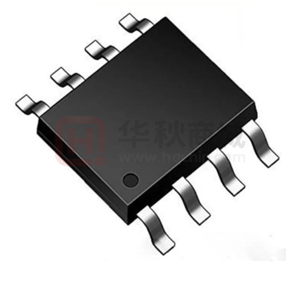


 工商网监
湘ICP备2023018690号
工商网监
湘ICP备2023018690号
