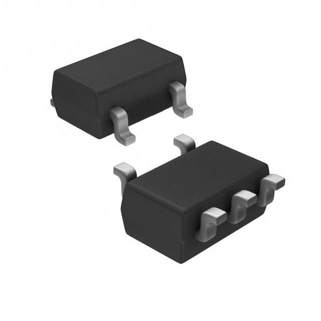
S-1111/1121 Series
www.sii-ic.com
N
HIGH RIPPLE-REJECTION LOW DROPOUT
CMOS VOLTAGE REGULATOR
Rev.5.1_00
DE
SI
G
© Seiko Instruments Inc., 2002-2015
The S-1111/1121 Series is a positive voltage regulator with a low dropout voltage, high-accuracy output
voltage, and low current consumption developed based on CMOS technology.
A built-in low on-resistance transistor provides a low dropout voltage and large output current, and a built-in
overcurrent protection circuit prevents the load current from exceeding the current capacity of the output
transistor. An ON/OFF circuit ensures a long battery life, and small SOT-23-5 package realize high-density
mounting. The lineup includes the S-1111 and S-1121 Series, which differ in pin configuration.
NE
R
FO
• Output current:
• Ripple rejection:
• Built-in overcurrent protection circuit:
• Built-in ON/OFF circuit:
• Operation temperature range:
• Lead-free, Sn 100%, halogen-free*2
1.5 V to 5.5 V, selectable in 0.1 V step
±1.0%
200 mV typ. (3.0 V output product, IOUT = 100 mA)
During operation: 35 μA typ., 65 μA max.
During power-off: 0.1 μA typ., 1.0 μA max.
Possible to output 150 mA (VIN ≥ VOUT(S) + 1.0 V)*1
70 dB typ. (f = 1.0 kHz)
Limits overcurrent of output transistor.
Ensures long battery life.
Ta = −40°C to +85°C
D
• Output voltage:
• Output voltage accuracy:
• Dropout voltage:
• Current consumption:
W
Features
DE
*1. Attention should be paid to the power dissipation of the package when the output current is large.
*2. Refer to “ Product Name Structure” for details.
MM
EN
Applications
Package
NO
T
RE
• SOT-23-5
CO
• Power supply for battery-powered device
• Power supply for personal communication device
• Power supply for home electric/electronic appliance
• Power supply for cellular phone
Seiko Instruments Inc.
1
�HIGH RIPPLE-REJECTION LOW DROPOUT CMOS VOLTAGE REGULATOR
Rev.5.1_00
S-1111/1121 Series
Block Diagram
N
*1
VOUT
DE
SI
G
VIN
Overcurrent
protection circuit
+
ON/OFF
circuit
R
Reference
voltage circuit
W
−
NE
ON/OFF
FO
VSS
D
*1. Parasitic diode
NO
T
RE
CO
MM
EN
DE
Figure 1
2
Seiko Instruments Inc.
�Rev.5.1_00
HIGH RIPPLE-REJECTION LOW DROPOUT CMOS VOLTAGE REGULATOR
S-1111/1121 Series
Product Name Structure
1.
DE
SI
G
N
• Users can select the product type, output voltage for the S-1111/1121 Series. Refer to “1. Product
name” regarding the contents of product name, “2. Package” regarding the package drawings, “3.
Product name list” regarding details of product name.
Product name
(1)
S-1111 Series
S-1111
x
xx
MC
-
xxx
TF
x
W
Environmental code
U: Lead-free (Sn 100%), halogen-free
G: Lead-free (for details, please contact our sales office)
Product code*2
NE
IC direction in tape specifications*1
FO
R
Package code
MC: SOT-23-5
D
Output voltage
15 to 55
(e.g., when the output voltage is 1.5 V, it is expressed
as 15.)
MM
EN
DE
Product type*3
A: ON/OFF pin negative logic
B: ON/OFF pin positive logic
NO
T
RE
CO
*1. Refer to the tape drawing.
*2. Refer to “3. Product name list”.
*3. Refer to “3. ON/OFF pin” in “ Operation”.
Seiko Instruments Inc.
3
�HIGH RIPPLE-REJECTION LOW DROPOUT CMOS VOLTAGE REGULATOR
Rev.5.1_00
S-1111/1121 Series
(2)
S-1121 Series
x
xx
MC
-
xxx
TF
x
N
S-1121
DE
SI
G
Environmental code
U: Lead-free (Sn 100%), halogen-free
G: Lead-free (for details, please contact our sales office)
IC direction in tape specifications*1
Package code
MC: SOT-23-5
W
Product code*2
NE
Output voltage
15 to 55
(e.g., when the output voltage is 1.5 V, it is expressed
as 15.)
Package
Package Name
Package
MP005-A-P-SD
Drawing Code
Tape
MP005-A-C-SD
NO
T
RE
CO
SOT-23-5
MM
EN
2.
DE
D
*1. Refer to the tape drawing.
*2. Refer to “3. Product name list”.
*3. Refer to “3. ON/OFF pin” in “ Operation”.
FO
R
Product type*3
A: ON/OFF pin negative logic
B: ON/OFF pin positive logic
4
Seiko Instruments Inc.
Reel
MP005-A-R-SD
�Rev.5.1_00
Product name list
(1)
S-1111 Series
N
3.
HIGH RIPPLE-REJECTION LOW DROPOUT CMOS VOLTAGE REGULATOR
S-1111/1121 Series
DE
SI
G
Table 1
NO
T
RE
CO
MM
EN
DE
D
FO
R
NE
W
Output Voltage
SOT-23-5
1.5V±1.0%
S-1111B15MC-NYATFx
1.6V±1.0%
S-1111B16MC-NYBTFx
1.7V±1.0%
S-1111B17MC-NYCTFx
1.8V±1.0%
S-1111B18MC-NYDTFx
1.9V±1.0%
S-1111B19MC-NYETFx
2.0V±1.0%
S-1111B20MC-NYFTFx
2.1V±1.0%
S-1111B21MC-NYGTFx
2.2V±1.0%
S-1111B22MC-NYHTFx
2.3V±1.0%
S-1111B23MC-NYITFx
2.4V±1.0%
S-1111B24MC-NYJTFx
2.5V±1.0%
S-1111B25MC-NYKTFx
2.6V±1.0%
S-1111B26MC-NYLTFx
2.7V±1.0%
S-1111B27MC-NYMTFx
2.8V±1.0%
S-1111B28MC-NYNTFx
2.9V±1.0%
S-1111B29MC-NYOTFx
3.0V±1.0%
S-1111B30MC-NYPTFx
3.1V±1.0%
S-1111B31MC-NYQTFx
3.2V±1.0%
S-1111B32MC-NYRTFx
3.3V±1.0%
S-1111B33MC-NYSTFx
3.4V±1.0%
S-1111B34MC-NYTTFx
3.5V±1.0%
S-1111B35MC-NYUTFx
3.6V±1.0%
S-1111B36MC-NYVTFx
3.7V±1.0%
S-1111B37MC-NYWTFx
3.8V±1.0%
S-1111B38MC-NYXTFx
3.9V±1.0%
S-1111B39MC-NYYTFx
4.0V±1.0%
S-1111B40MC-NYZTFx
4.1V±1.0%
S-1111B41MC-NZATFx
4.2V±1.0%
S-1111B42MC-NZBTFx
4.3V±1.0%
S-1111B43MC-NZCTFx
4.4V±1.0%
S-1111B44MC-NZDTFx
4.5V±1.0%
S-1111B45MC-NZETFx
4.6V±1.0%
S-1111B46MC-NZFTFx
4.7V±1.0%
S-1111B47MC-NZGTFx
-
4.75V±1.0%
4.8V±1.0%
S-1111B48MC-NZHTFx
4.9V±1.0%
S-1111B49MC-NZITFx
5.0V±1.0%
S-1111B50MC-NZJTFx
5.1V±1.0%
S-1111B51MC-NZKTFx
5.2V±1.0%
S-1111B52MC-NZLTFx
5.3V±1.0%
S-1111B53MC-NZMTFx
5.4V±1.0%
S-1111B54MC-NZNTFx
5.5V±1.0%
S-1111B55MC-NZOTFx
Remark 1. Please contact our sales office for type A products.
2. x: G or U
3. Please select products of environmental code = U for Sn 100%, halogen-free products.
Seiko Instruments Inc.
5
�HIGH RIPPLE-REJECTION LOW DROPOUT CMOS VOLTAGE REGULATOR
Rev.5.1_00
S-1111/1121 Series
S-1121 Series
Table
2
N
(2)
NO
T
RE
CO
MM
EN
DE
D
FO
R
NE
W
DE
SI
G
Output Voltage
SOT-23-5
1.5V±1.0%
S-1121B15MC-N2ATFx
1.6V±1.0%
S-1121B16MC-N2BTFx
1.7V±1.0%
S-1121B17MC-N2CTFx
1.8V±1.0%
S-1121B18MC-N2DTFx
1.9V±1.0%
S-1121B19MC-N2ETFx
2.0V±1.0%
S-1121B20MC-N2FTFx
2.1V±1.0%
S-1121B21MC-N2GTFx
2.2V±1.0%
S-1121B22MC-N2HTFx
2.3V±1.0%
S-1121B23MC-N2ITFx
2.4V±1.0%
S-1121B24MC-N2JTFx
2.5V±1.0%
S-1121B25MC-N2KTFx
2.6V±1.0%
S-1121B26MC-N2LTFx
2.7V±1.0%
S-1121B27MC-N2MTFx
2.8V±1.0%
S-1121B28MC-N2NTFx
2.9V±1.0%
S-1121B29MC-N2OTFx
3.0V±1.0%
S-1121B30MC-N2PTFx
3.1V±1.0%
S-1121B31MC-N2QTFx
3.2V±1.0%
S-1121B32MC-N2RTFx
3.3V±1.0%
S-1121B33MC-N2STFx
3.4V±1.0%
S-1121B34MC-N2TTFx
3.5V±1.0%
S-1121B35MC-N2UTFx
3.6V±1.0%
S-1121B36MC-N2VTFx
3.7V±1.0%
S-1121B37MC-N2WTFx
3.8V±1.0%
S-1121B38MC-N2XTFx
3.9V±1.0%
S-1121B39MC-N2YTFx
4.0V±1.0%
S-1121B40MC-N2ZTFx
4.1V±1.0%
S-1121B41MC-N3ATFx
4.2V±1.0%
S-1121B42MC-N3BTFx
4.3V±1.0%
S-1121B43MC-N3CTFx
4.4V±1.0%
S-1121B44MC-N3DTFx
4.5V±1.0%
S-1121B45MC-N3ETFx
4.6V±1.0%
S-1121B46MC-N3FTFx
4.7V±1.0%
S-1121B47MC-N3GTFx
4.75V±1.0%
S-1121B4HMC-N3PTFx
4.8V±1.0%
S-1121B48MC-N3HTFx
4.9V±1.0%
S-1121B49MC-N3ITFx
5.0V±1.0%
S-1121B50MC-N3JTFx
5.1V±1.0%
S-1121B51MC-N3KTFx
5.2V±1.0%
S-1121B52MC-N3LTFx
5.3V±1.0%
S-1121B53MC-N3MTFx
5.4V±1.0%
S-1121B54MC-N3NTFx
5.5V±1.0%
S-1121B55MC-N3OTFx
Remark 1. Please contact our sales office for type A products.
2. x: G or U
3. Please select products of environmental code = U for Sn 100%, halogen-free products.
6
Seiko Instruments Inc.
�Rev.5.1_00
HIGH RIPPLE-REJECTION LOW DROPOUT CMOS VOLTAGE REGULATOR
S-1111/1121 Series
Pin Configuration
Table
SOT-23-5
Top view
N
4
3
W
2
Table
4
(S-1121 Series)
Pin No.
Symbol
Description
1
VOUT
Output voltage pin
2
VSS
GND pin
3
VIN
Input voltage pin
4
ON/OFF
ON/OFF pin
5
NC*1
No connection
*1. The NC pin is electrically open.
The NC pin can be connected to VIN pin or VSS pin.
NE
1
(S-1111 Series)
Pin No.
Symbol
Description
1
VIN
Input voltage pin
2
VSS
GND pin
3
ON/OFF
ON/OFF pin
4
NC*1
No connection
5
VOUT
Output voltage pin
*1. The NC pin is electrically open.
The NC pin can be connected to VIN pin or VSS pin.
DE
SI
G
5
3
R
2
NO
T
RE
CO
MM
EN
DE
D
FO
Figure
Seiko Instruments Inc.
7
�HIGH RIPPLE-REJECTION LOW DROPOUT CMOS VOLTAGE REGULATOR
Rev.5.1_00
S-1111/1121 Series
Absolute Maximum Ratings
Table
Output voltage
Power dissipation
PD
N
Symbol
VIN
VON/OFF
VOUT
(Ta = 25 °C unless otherwise specified)
Absolute Maximum Rating
Unit
V
VSS − 0.3 to VSS + 7
V
VSS − 0.3 to VIN + 0.3
V
VSS − 0.3 to VIN + 0.3
300 (When not mounted on board)
mW
600*1
mW
−40 to +85
°C
−40 to +125
°C
DE
SI
G
Item
Input voltage
5
NE
W
Operation ambient temperature
Topr
Storage temperature
Tstg
*1. When mounted on board
[Mounted on board]
(1) Board size : 114.3 mm × 76.2 mm × t1.6 mm
(2) Board name : JEDEC STANDARD51-7
R
FO
700
600
500
200
100
DE
300
D
400
MM
EN
Power dissipation (PD) [mW]
Caution The absolute maximum ratings are rated values exceeding which the product could suffer
physical damage. These values must therefore not be exceeded under any conditions.
0
100
150
50
Ambient temperature (Ta) [°C]
Power Dissipation of Package (When Mounted on Board)
NO
T
RE
CO
Figure 3
0
8
Seiko Instruments Inc.
�Rev.5.1_00
HIGH RIPPLE-REJECTION LOW DROPOUT CMOS VOLTAGE REGULATOR
S-1111/1121 Series
Electrical Characteristics
Table
6
Condition
Min.
mA
V
V
V
V
V
3
1
1
1
1
1
0.05
0.2
%/V
1
⎯
20
40
mV
1
⎯
±100
⎯
ppm
/ °C
1
⎯
35
65
μA
2
⎯
0.1
1.0
1
2
2.0
⎯
6.5
V
⎯
1.5
⎯
⎯
V
4
⎯
⎯
0.3
V
4
VIN = 6.5 V, VON/OFF = 6.5 V
−0.1
⎯
0.1
μA
4
VIN = 6.5 V, VON/OFF = 0 V
−0.1
⎯
0.1
μA
4
⎯
70
⎯
dB
5
⎯
250
⎯
mA
3
Line regulation
ΔVOUT1
ΔVIN• VOUT
Load regulation
ΔVOUT2
VIN
VIN ≥ VOUT(S) + 1.0 V
IOUT = 100 mA
1.5 V ≤ VOUT(S) ≤ 1.9 V
2.0 V ≤ VOUT(S) ≤ 2.4 V
2.5 V ≤ VOUT(S) ≤ 2.7 V
2.8 V ≤ VOUT(S) ≤ 3.3 V
3.4 V ≤ VOUT(S) ≤ 5.5 V
VOUT(S) + 0.5 V ≤ VIN ≤ 6.5 V,
IOUT = 30 mA
VIN = VOUT(S) + 1.0 V,
1.0 mA ≤ IOUT ≤ 80 mA
VIN = VOUT(S) + 1.0 V, IOUT = 10 mA,
−40°C ≤ Ta ≤ 85°C
VIN = VOUT(S) + 1.0 V, ON/OFF pin = ON,
no load
VIN = VOUT(S) + 1.0 V, ON/OFF pin = OFF,
no load
⎯
VSH
VIN = VOUT(S) + 1.0 V, RL = 1.0 kΩ
VSL
VIN = VOUT(S) + 1.0 V, RL = 1.0 kΩ
ISH
Short-circuit current
Ishort
R
FO
D
DE
MM
EN
RR
Ripple rejection
NE
IOUT
Vdrop
ISL
⎯
⎯
0.60
0.35
0.24
0.20
0.17
Output current*2
Dropout voltage*3
ISS2
VOUT(S)
Test
Circuit
1
VIN = VOUT(S) + 1.0 V, IOUT = 30 mA
ISS1
VOUT(S)
× 0.99
150*5
⎯
⎯
⎯
⎯
⎯
Unit
V
VOUT(E)
ΔVOUT
ΔTa • VOUT
Max.
VOUT(S)
× 1.01
⎯
1.40
0.70
0.35
0.30
0.26
Output voltage*1
Output voltage
*4
temperature coefficient
Current consumption
during operation
Current consumption
during power-off
Input voltage
ON/OFF pin
input voltage “H”
ON/OFF pin
input voltage “L”
ON/OFF pin
input current “H”
ON/OFF pin
input current “L”
Typ.
DE
SI
G
Symbol
W
Item
N
(Ta = 25 °C unless otherwise specified)
VIN = VOUT(S) + 1.0 V, f = 1.0 kHz,
ΔVrip = 0.5 Vrms, IOUT = 30 mA
VIN = VOUT(S) + 1.0 V, ON/OFF pin = ON,
VOUT = 0 V
NO
T
RE
CO
*1. VOUT(S): Set output voltage
VOUT(E): Actual output voltage
Output voltage when fixing IOUT(= 30 mA) and inputting VOUT(S) + 1.0 V
*2. The output current at which the output voltage becomes 95% of VOUT(E) after gradually increasing the output current.
*3. Vdrop = VIN1 − (VOUT3 × 0.98)
VOUT3 is the output voltage when VIN = VOUT(S) + 1.0 V and IOUT = 100 mA.
VIN1 is the input voltage at which the output voltage becomes 98% of VOUT3 after gradually decreasing the input
voltage.
*4. A change in the temperature of the output voltage [mV/°C] is calculated using the following equation.
ΔV
ΔVOUT
[mV/°C]*1 = VOUT(S) [V]*2 × ΔTa •OUT
[ppm/°C]*3 ÷ 1000
ΔTa
VOUT
*1. Change in temperature of output voltage
*2. Set output voltage
*3. Output voltage temperature coefficient
*5. The output current can be at least this value.
Due to restrictions on the package power dissipation, this value may not be satisfied. Attention should be paid to the
power dissipation of the package when the output current is large.
This specification is guaranteed by design.
Seiko Instruments Inc.
9
�HIGH RIPPLE-REJECTION LOW DROPOUT CMOS VOLTAGE REGULATOR
Rev.5.1_00
S-1111/1121 Series
Test Circuits
1.
+
V
VSS
+
DE
SI
G
ON/OFF
A
N
VOUT
VIN
Set to ON
+
A
VOUT
VIN
ON/OFF
W
2.
4
VSS
NE
Figure
Set to
VIN or GND
VIN
ON/OFF
R
+
VOUT
A
V
VSS
+
D
3.
5
FO
Figure
DE
Set to ON
4.
VIN
RE
NO
T
10
A
ON/OFF
CO
+
5.
6
MM
EN
Figure
VOUT
VSS
Figure
VIN
+
V
RL
7
VOUT
+
ON/OFF
VSS
V
RL
Set to ON
Figure
8
Seiko Instruments Inc.
�Rev.5.1_00
HIGH RIPPLE-REJECTION LOW DROPOUT CMOS VOLTAGE REGULATOR
S-1111/1121 Series
Standard Circuit
Output
Input
N
*1
CIN
VOUT
*2
CL
ON/OFF
VSS
GND
Single GND
DE
SI
G
VIN
9
NE
Figure
W
*1. CIN is a capacitor for stabilizing the input.
*2. A tantalum capacitor (2.2 μF or more) can be used.
R
Caution The above connection diagram and constant will not guarantee successful operation.
Perform thorough evaluation using the actual application to set the constant.
1.0 μF or more
2.2 μF or more (tantalum capacitor)
D
Input capacitor (CIN):
Output capacitor (CL):
FO
Condition of Application
NO
T
RE
CO
MM
EN
DE
Caution Generally a series regulator may cause oscillation, depending on the selection of external
parts. Check that no oscillation occurs with the application using the above capacitor.
Seiko Instruments Inc.
11
�HIGH RIPPLE-REJECTION LOW DROPOUT CMOS VOLTAGE REGULATOR
Rev.5.1_00
S-1111/1121 Series
Explanation of Terms
1. Low dropout voltage regulator
N
This voltage regulator has the low dropout voltage due to its built-in low on-resistance transistor.
DE
SI
G
2. Output voltage (VOUT)
The accuracy of the output voltage is ensured at ±1.0% under the specified conditions of fixed input
voltage*1, fixed output current, and fixed temperature.
Differs depending the product.
Caution
If the above conditions change, the output voltage value may vary and exceed the
accuracy range of the output voltage. Refer to “ Electrical Characteristics” and “
Characteristics (Typical Data)” for details.
W
*1.
ΔVOUT1
ΔVIN • VOUT
NE
3. Line regulation
Indicates the dependency of the output voltage on the input voltage. That is, the value shows how
much the output voltage changes due to a change in the input voltage with the output current remaining
unchanged.
R
4. Load regulation (ΔVOUT2)
D
5. Dropout voltage (Vdrop)
FO
Indicates the dependency of the output voltage on the output current. That is, the value shows how
much the output voltage changes due to a change in the output current with the input voltage remaining
unchanged.
NO
T
RE
CO
MM
EN
Vdrop = VIN1 − (VOUT3 × 0.98)
DE
Indicates the difference between input voltage (VIN1) and the output voltage when; decreasing input
voltage (VIN) gradually until the output voltage has dropped out to the value of 98% of output voltage
(VOUT3), which is at VIN = VOUT(S) + 1.0 V.
12
Seiko Instruments Inc.
�Rev.5.1_00
HIGH RIPPLE-REJECTION LOW DROPOUT CMOS VOLTAGE REGULATOR
S-1111/1121 Series
ΔVOUT
ΔTa • VOUT
6. Output voltage temperature coefficient
DE
SI
G
N
The shaded area in Figure 10 is the range where VOUT varies in the operation temperature range when
the output voltage temperature coefficient is ±100 ppm/°C.
Example of S-1111/1121B28 typ. product
VOUT
[V]
+0.28 mV/°C
W
VOUT(E)*1
+25
+85
Ta [°C]
R
−40
NE
−0.28 mV/°C
FO
*1. VOUT(E) is the value of the output voltage measured at Ta = +25°C.
Figure
10
NO
T
RE
CO
MM
EN
DE
D
A change in the temperature of the output voltage [mV/°C] is calculated using the following equation.
ΔV
ΔVOUT
[mV/°C]*1 = VOUT(S) [V]*2 × ΔTa •OUT
[ppm/°C]*3 ÷ 1000
ΔTa
VOUT
*1. Change in temperature of output voltage
*2. Set output voltage
*3. Output voltage temperature coefficient
Seiko Instruments Inc.
13
�HIGH RIPPLE-REJECTION LOW DROPOUT CMOS VOLTAGE REGULATOR
Rev.5.1_00
S-1111/1121 Series
Operation
1. Basic operation
N
Figure 11 shows the block diagram of the S-1111/1121 Series.
DE
SI
G
The error amplifier compares the reference voltage (Vref) with feedback voltage (Vfb), which is the output
voltage resistance-divided by feedback resistors (Rs and Rf). It supplies the gate voltage necessary to
maintain the constant output voltage which is not influenced by the input voltage and temperature
change, to the output transistor.
VIN
*1
W
Current
supply
NE
Error
amplifier
−
Vref
Rf
FO
R
+
Reference voltage
circuit
D
Rs
Parasitic diode
MM
EN
2. Output transistor
Vfb
DE
VSS
*1.
VOUT
Figure
11
NO
T
RE
CO
In the S-1111/1121 Series, a low on-resistance P-channel MOS FET is used as the output transistor.
Be sure that VOUT does not exceed VIN + 0.3 V to prevent the voltage regulator from being damaged due
to reverse current flowing from the VOUT pin through a parasitic diode to the VIN pin, when the potential
of VOUT became higher than VIN.
14
Seiko Instruments Inc.
�Rev.5.1_00
HIGH RIPPLE-REJECTION LOW DROPOUT CMOS VOLTAGE REGULATOR
S-1111/1121 Series
3. ON/OFF pin
This pin starts and stops the regulator.
Internal Circuit
Operate
Stop
Stop
Operate
VOUT Pin Voltage
Set value
VSS level
VSS level
Set value
Current Consumption
ISS1
ISS2
ISS2
ISS1
W
ON/OFF Pin
“L”: ON
“H”: OFF
“L”: OFF
“H”: ON
R
Product Type
A
A
B
B
7
NE
Table
DE
SI
G
N
When the ON/OFF pin is set to OFF level, the entire internal circuit stops operating, and the built-in
P-channel MOS FET output transistor between the VIN pin and the VOUT pin is turned off, reducing
current consumption significantly. The VOUT pin becomes the VSS level due to the internally divided
resistance of several hundreds kΩ between the VOUT pin and the VSS pin.
The structure of the ON/OFF pin is as shown in Figure 12. Since the ON/OFF pin is neither pulled down
nor pulled up internally, do not use it in the floating status. In addition, note that the current consumption
increases if a voltage of 0.3 V to VIN – 0.3 V is applied to the ON/OFF pin. When not using the ON/OFF
pin, connect it to the VSS pin in the product A type, and connect it to the VIN pin in B type.
ON/OFF
Figure
MM
EN
VSS
DE
D
FO
VIN
12
Selection of Output Capacitor (CL)
NO
T
RE
CO
The S-1111/1121 Series performs phase compensation using the internal phase compensator in the IC and the
ESR (Equivalent Series Resistance) of the output capacitor to enable stable operation independent of changes
in the output load. Therefore, always place a capacitor (CL) of 2.2 μF or more between the VOUT pin and the
VSS pin.
For stable operation of the S-1111/1121 Series, it is essential to employ a capacitor whose ESR is within an
optimum range. Using a capacitor whose ESR is outside the optimum range (approximately 0.5 Ω to 5 Ω),
whether larger or smaller, may cause an unstable output, resulting in oscillation. For this reason, a tantalum
electrolytic capacitor is recommended.
When a ceramic capacitor or an OS capacitor with a low ESR is used, it is necessary to connect an additional
resistor that serves as the ESR in series with the output capacitor. The required resistance value is
approximately 0.5 Ω to 5 Ω, which varies depending on the usage conditions, so perform sufficient evaluation
for selection. Ordinarily, around 1.0 Ω is recommended.
Note that an aluminum electrolytic capacitor may increase the ESR at a low temperature, causing oscillation.
When using this kind of capacitor, perform thorough evaluation, including evaluation of temperature
characteristics.
Seiko Instruments Inc.
15
�HIGH RIPPLE-REJECTION LOW DROPOUT CMOS VOLTAGE REGULATOR
Rev.5.1_00
S-1111/1121 Series
Precautions
NO
T
RE
CO
MM
EN
DE
D
FO
R
NE
W
DE
SI
G
N
• Wiring patterns for the VIN pin, the VOUT pin and GND should be designed so that the impedance is
low. When mounting an output capacitor between the VOUT pin and the VSS pin (CL) and a capacitor
for stabilizing the input between the VIN pin and the VSS pin (CIN), the distance from the capacitors to
these pins should be as short as possible.
• Note that generally the output voltage may increase when a series regulator is used at low load current
(1.0 mA or less).
• The S-1111/1121 Series performs phase compensation by using an internal phase compensator and
the ESR of an output capacitor. Therefore, always place a capacitor of 2.2 μF or more between the
VOUT pin and the VSS pin. A tantalum type capacitor is recommended. Moreover, to secure stable
operation of the S-1111/1121 Series, it is necessary to employ a capacitor with an ESR within an
optimum range (0.5 Ω to 5 Ω). Using a capacitor whose ESR is outside the optimum range
(approximately 0.5 Ω to 5 Ω), whether larger or smaller, may cause an unstable output, resulting in
oscillation. Perform sufficient evaluation under the actual usage conditions for selection, including
evaluation of temperature characteristics.
• The voltage regulator may oscillate when the impedance of the power supply is high and the input
capacitance is small or an input capacitor is not connected.
• Overshoot may occur in the output voltage momentarily if the voltage is rapidly raised at power-on or
when the power supply fluctuates. Sufficiently evaluate the output voltage at power-on with the actual
device.
• The application conditions for the input voltage, the output voltage, and the load current should not
exceed the package power dissipation.
• Do not apply an electrostatic discharge to this IC that exceeds the performance ratings of the built-in
electrostatic protection circuit.
• In determining the output current, attention should be paid to the output current value specified in Table
6 in “ Electrical Characteristics” and footnote *5 of the table.
• SII claims no responsibility for any disputes arising out of or in connection with any infringement by
products including this IC of patents owned by a third party.
16
Seiko Instruments Inc.
�Rev.5.1_00
HIGH RIPPLE-REJECTION LOW DROPOUT CMOS VOLTAGE REGULATOR
S-1111/1121 Series
Characteristics (Typical Data)
N
Remark The following, which describes the S-1111 Series as the typical product, shows typical data
common to the S-1121 Series.
2
4
3.5
3
2.5
2
1.5
1
0.5
0
2.0 V
1
VOUT [V]
VOUT [V]
1.5
VIN = 1.8 V
0.5
6.5 V
2.5 V
0
100
200
300
400
500
600
0
IOUT [mA]
200
300
400
500
600
R
6
6.5 V
6.0 V
3
2
1
0
100
200
300
400
500
IOUT [mA]
1.6
600
MM
EN
(2) Output voltage vs. Input voltage
S-1111B15 (Ta = 25 °C)
DE
VIN = 5.3 V
0
50 mA
S-1111B30 (Ta = 25 °C)
3.05
IOUT = 1 mA
1.55
30 mA
1.5
1.45
1.4
2
2.5
50 mA
IOUT = 1 mA
3
2.95
30 mA
80 mA
2.9
2.85
2.8
3
3.5
2.5
RE
1.5
CO
80 mA
1
Remark In determining the output current, attention
should be paid to the following.
1) The minimum output current value and
footnote *5 of Table 6 in the “ Electrical
Characteristics”
2) The package power dissipation
D
5.5 V
VOUT [V]
4
FO
5
VOUT [V]
100
3.5 V
VIN = 3.3 V
IOUT [mA]
S-1111B50 (Ta = 25 °C)
VOUT [V]
6.5 V
NE
0
4.0 V
W
2.5
DE
SI
G
(1) Output Voltage vs. Output current (when load current increases)
S-1111B15 (Ta = 25 °C)
S-1111B30 (Ta = 25 °C)
VIN [V]
3
3.5
4
4.5
5
VIN [V]
5.1
5.08
5.06
5.04
5.02
5 30 mA
4.98
4.96
4.94
4.92
4.9
4.5
5
NO
T
VOUT [V]
S-1111B50 (Ta = 25 °C)
IOUT = 1 mA
50 mA
80 mA
5.5
6
6.5
7
VIN [V]
Seiko Instruments Inc.
17
�HIGH RIPPLE-REJECTION LOW DROPOUT CMOS VOLTAGE REGULATOR
Rev.5.1_00
S-1111/1121 Series
N
0.45
0.4
0.35
0.3
0.25
0.2
0.15
0.1
0.05
0
S-1111B30
0.3
25°C
85°C
85°C
0.2
-40°C
0.15
0
50
100
150
200
0
NE
0.25
25°C
R
0.1
−40°C
FO
Vdrop [V]
85°C
0.15
0.05
100
150
200
DE
IOUT [mA]
D
0
50
MM
EN
150 mA
100 mA
50 mA
30 mA
10 mA
0
1
CO
Vdrop [V]
(4) Dropout voltage vs. Set output voltage
0.4
0.35
0.3
0.25
0.2
0.15
0.1
0.05
0
2
3
100
IOUT [mA]
S-1111B50
0
50
W
IOUT [mA]
0.2
25°C
-40°C
0.1
0.05
0
4
5
6
7
NO
T
RE
VOUT(S) [V]
18
DE
SI
G
0.25
Vdrop [V]
Vdrop [V]
(3) Dropout voltage vs. Output current
S-1111B15
Seiko Instruments Inc.
150
200
�3.1
1.55
3.05
1.5
1.45
N
S-1111B30
1.6
VOUT [V]
VOUT [V]
(5) Output voltage vs. Ambient temperature
S-1111B15
3
2.95
1.4
-40
-20
0
20
40
60
80
2.9
-40
100
60
80
100
NE
R
20
40
60
80
100
DE
(6) Current consumption vs. Input voltage
S-1111B15
MM
EN
S-1111B30
25°C
85°C
0
S-1111B50
2
CO
−40°C
4
VIN [V]
6
8
45
40
35
30
25
20
15
10
5
0
25°C
85°C
−40°C
0
2
4
VIN [V]
6
8
RE
ISS1 [μA]
40
FO
0
Ta [°C]
85°C
NO
T
ISS1 [μA]
20
D
-40 -20
ISS1 [μA]
VOUT [V]
5.1
5.08
5.06
5.04
5.02
5
4.98
4.96
4.94
4.92
4.9
45
40
35
30
25
20
15
10
5
0
0
Ta [°C]
S-1111B50
45
40
35
30
25
20
15
10
5
0
-20
W
Ta [°C]
DE
SI
G
Rev.5.1_00
HIGH RIPPLE-REJECTION LOW DROPOUT CMOS VOLTAGE REGULATOR
S-1111/1121 Series
0
2
−40°C
4
VIN [V]
25°C
6
8
Seiko Instruments Inc.
19
�HIGH RIPPLE-REJECTION LOW DROPOUT CMOS VOLTAGE REGULATOR
Rev.5.1_00
S-1111/1121 Series
(7) Ripple rejection
S-1111B15 (Ta = 25 °C)
S-1111B30 (Ta = 25 °C)
VIN = 4.0 V, COUT = 2.2 μF
Ripple Rejection [dB]
60
40
30 mA
20
0
50 mA
10
100
1k
10 k
Frequency [Hz]
100 k
80
60
40
30 mA
20
0
1M
S-1111B50 (Ta = 25 °C)
VIN = 6.0 V, COUT = 2.2 μF
IOUT = 1 mA
40
50 mA
1k
10 k
1M
NO
T
RE
CO
MM
EN
Frequency [Hz]
100 k
D
30 mA
20
100
20
10
FO
60
10
50 mA
R
80
DE
Ripple Rejection [dB]
100
0
IOUT = 1 mA
100
1k
10 k
Frequency [Hz]
W
IOUT = 1 mA
NE
Ripple Rejection [dB]
80
DE
SI
G
100
100
N
VIN = 2.5 V, COUT = 2.2 μF
Seiko Instruments Inc.
100 k
1M
�Rev.5.1_00
HIGH RIPPLE-REJECTION LOW DROPOUT CMOS VOLTAGE REGULATOR
S-1111/1121 Series
Reference Data
(1) Input transient response characteristics
5
3.02
4
3.015
V IN
3.01
3
V OUT
3.005
2
3
1
3
2.995
0
2.995
20
40
60
80
100 120 140 160 180
-20
0
t [μs]
0
-50
3
2.95
4
6
8
10
VOUT
-100
14
-150
18
12
16
t [μs]
R
VOUT [V]
IOUT
100
3.1
50
FO
50
D
3.1
IOUT [mA]
100
150
3.15
IOUT
3.05
0
3
-50
2.95
-100
VOUT
2.9
-2
DE
VOUT [V]
3.15
2
0
100 120 140 160 180
3.2
150
0
80
VIN = 4.0 V, COUT = 4.7 μF, CIN = 1.0 μF,
IOUT = 50 mA ↔100 mA
3.2
-2
60
1
NE
VIN = 4.0 V, COUT = 2.2 μF, CIN = 1.0 μF,
IOUT = 50 mA ↔100 mA
2.9
40
2
t [μs]
(2) Load transient response characteristics
3.05
20
3
VOUT
0
2
4
6
8
10
12
14
16
IOUT [mA]
0
3.005
4
W
-20
VIN
3.01
5
VIN [V]
3.02
3.015
6
DE
SI
G
3.025
VOUT [V]
6
N
IOUT = 30 mA, tr = tf = 5.0 μs, COUT = 4.7 μF, CIN = 0 μF
3.025
VIN [V]
VOUT [V]
IOUT = 30 mA, tr = tf = 5.0 μs, COUT = 2.2 μF, CIN = 0 μF
-150
18
t [μs]
S-1111B30 (Ta = 25 °C)
VIN = 2.5 V, COUT = 2.2 μF, CIN = 1.0 μF
VON/OFF
1.5
0
-10
0
10
20
4
1
3
0
-1
30
40
50
60
70
80
90
6
4
VON/OFF
2
2
0
VOUT
1
-2
-2
0
-4
-3
-1
-10
RE
-0.5
2
VOUT
1
0.5
5
CO
VOUT [V]
2
3
VON/OFF [V]
2.5
VIN = 4.0 V, COUT = 2.2 μF, CIN = 1.0 μF
VOUT [V]
S-1111B15 (Ta = 25 °C)
t [μs]
0
10
20
30
40
50
60
70
80
90
VON/OFF [V]
MM
EN
(3) ON/OFF pin transient response characteristics
-6
t [μs]
S-1111B50 (Ta = 25 °C)
NO
T
VIN = 6.0 V, COUT = 2.2 μF, CIN = 1.0 μF
7
8
VON/OFF
6
VOUT [V]
5
4
4
2
VOUT
3
0
2
-2
1
-4
0
-1 -10
VON/OFF [V]
6
-6
0
10
20
30
40
50
60
70
80
90 -8
t [μs]
Seiko Instruments Inc.
21
�N
DE
SI
G
2.9±0.2
1.9±0.2
4
2
3
+0.1
0.16 -0.06
DE
0.95±0.1
D
FO
R
1
NE
W
5
No. MP005-A-P-SD-1.2
NO
T
RE
CO
MM
EN
0.4±0.1
TITLE
No.
SOT235-A-PKG Dimensions
MP005-A-P-SD-1.2
SCALE
UNIT
mm
Seiko Instruments Inc.
�4.0±0.1(10 pitches:40.0±0.2)
+0.1
2.0±0.05
0.25±0.1
+0.2
W
DE
SI
G
N
ø1.5 -0
4.0±0.1
NE
ø1.0 -0
5
Feed direction
No. MP005-A-C-SD-2.1
NO
T
RE
CO
4
MM
EN
3 2 1
DE
D
FO
R
3.2±0.2
1.4±0.2
TITLE
SOT235-A-Carrier Tape
No.
MP005-A-C-SD-2.1
SCALE
UNIT
mm
Seiko Instruments Inc.
�D
FO
R
NE
W
DE
SI
G
N
12.5max.
9.0±0.3
DE
MM
EN
Enlarged drawing in the central part
(60°)
CO
(60°)
ø13±0.2
NO
T
RE
No. MP005-A-R-SD-1.1
SOT235-A-Reel
TITLE
No.
MP005-A-R-SD-1.1
SCALE
QTY.
UNIT
mm
Seiko Instruments Inc.
3,000
�N
DE
SI
G
W
NE
R
FO
D
DE
MM
EN
www.sii-ic.com
The information described herein is subject to change without notice.
•
When the products described herein are regulated products subject to the Wassenaar Arrangement or other
agreements, they may not be exported without authorization from the appropriate governmental authority.
•
Use of the information described herein for other purposes and/or reproduction or copying without the
express permission of Seiko Instruments Inc. is strictly prohibited.
•
The products described herein cannot be used as part of any device or equipment affecting the human
body, such as exercise equipment, medical equipment, security systems, gas equipment, vehicle equipment,
in-vehicle equipment, aviation equipment, aerospace equipment, and nuclear-related equipment, without prior
written permission of Seiko Instruments Inc.
•
•
The products described herein are not designed to be radiation-proof.
CO
•
•
NO
T
RE
Seiko Instruments Inc. is not responsible for any problems caused by circuits or diagrams described herein
whose related industrial properties, patents, or other rights belong to third parties. The application circuit
examples explain typical applications of the products, and do not guarantee the success of any specific
mass-production design.
Although Seiko Instruments Inc. exerts the greatest possible effort to ensure high quality and reliability, the
failure or malfunction of semiconductor products may occur. The user of these products should therefore
give thorough consideration to safety design, including redundancy, fire-prevention measures, and
malfunction prevention, to prevent any accidents, fires, or community damage that may ensue.
�


 工商网监
湘ICP备2023018690号
工商网监
湘ICP备2023018690号
