LX21EVK01
Channel Link III Ser/Des
Evaluation Kit
Rev 1.0
Oct, 2010
General Description
The LX21EVK01 is designed to allow for easy evaluation of the DS92LX2121 and DS92LX2122 Channel Link III Ser/Des. This
kit allows for 2 basic methods of evaluation:
1)
Users may apply parallel clock, data and I2C commands, and evaluate the power, jitter and cable performance of the
Ser/Des. Or,
2)
Apply only a parallel clock and enable BIST mode. This allows the user to easily evaluate the serial link and check
device feature functionality such as receive equalization, SSCG, etc.
The LX16EVK01 boards uses USB connectors as the serial Channel Link III inputs/outputs. SMA connectors can also be
attached and configured for serial input/output if other types of the cable are desired.
Features
•
•
•
•
•
•
•
•
•
•
•
20 – 50 MHz support for up to 800 Mbps (default configuration)
LVCMOS parallel interface: 21-bit data (default) + clock + 2 upstream GPIO
High speed forward channel + bi-directional control channel + back channel GPIO serialized to 1 pair
AC Coupled STP Interconnect up to 10 meters in length
Selectable receive equalization, SSCG, and deserializer output slew rate
Integrated serial terminations
@ Speed link BIST Mode and reporting pin
I2C compatible Serial Control Bus
Power down mode minimizes power dissipation
Randomized, DC-balanced and Scrambled data stream with CRC
>8 kV HBM
Applications
•
•
•
Industrial Displays
Machine Vision
Medical Imaging
Ordering Information
PART: LX21EVK01
Demo boards:
Tx: DS92LX2121-EVK
Rx: DS92LX2122-EVK
national.com
© National Semiconductor Corporation 2009
1
Printed in U.S.
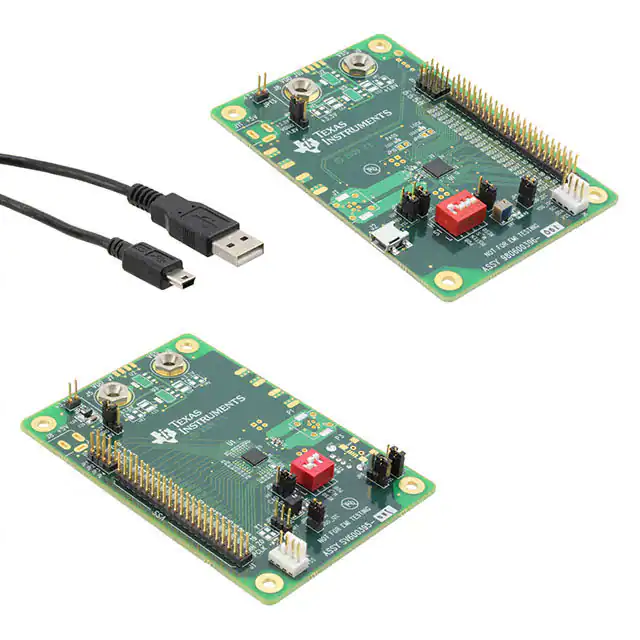
�Quick Start Guide:
DS92LX2121 Tx Board:
1.
Connect 3.3V DC power and ground of the board to JP12 from the power supply (3.3V on left pin, ground on right
pin). Connect 1.8V DC power and ground of the board to the J5 and J6 from the power supply respectively.
2.
Attach the USB cable to the TX board (DS92LX2121) output and to an RX board (DS92LX2122) input.
3.
Attach parallel data and clock to the TX board at connector J1. This is typically done with a flat ribbon cable (not
supplied).
DS92LX2122 Rx Board
4.
Connect 3.3V DC power and ground of the board to JP13 from the power supply (3.3V on left pin, ground on right
pin). Connect 1.8V DC power and ground of the board to the J8 and J9 from the power supply respectively.
5.
Attach the USB cable to the RX board (DS92LX2122) input from a TX board (DS92LX2121) output.
6.
Attach parallel data and clock output to the RX board at connector J7. This is typically done with a flat ribbon cable
(not supplied).
Jumpers and switches on both the TX and RX boards have been configured at the factory; they should not require any
changes for immediate operation. See the datasheet for more details.
national.com
© National Semiconductor Corporation 2009
2
Printed in U.S.
�Tx Board Configuration Settings
Component
Name
Function
Power Connections
J8
5V DC
J5
1.8V DC
J6
VSS
JP12
3.3V DC
JP11
VDDIO
Input and Output Connections
44 position wall
header (DIN0 –
DIN20, PCLK)
J1
JP1 - JP4
Optional 5V DC Power Jack. Note: unpopulated by default
1.8V VDD Power.
Ground.
3.3V VDD Power (left header pin), Ground (right header pin)
Input voltage select. Jumper set to 3.3V by default.
Connect to data input.
P2
GPO0 - GPO3
USB Connector
(Type-A Female)
Optional general purpose back channel data output
Connect to Channel Link II output (default).
J2 and J3
SMA Connectors
Connect to Channel Link II output. Note: unpopulated by default
Control Connections
S1:1
PDB
Power down mode input.
PDB = H, Serializer is enabled (default)
PDB = L, Serializer is in power-down mode
I2C Mode Select.
M_S = H, Slave Mode – device receives clock and data from local master
M_S = L, Master Mode – device generates and drives the clock line
S1:2
M_S
S1:3
RESO
JP8 and VR1
CAD
JP9 and J4
I2C Interface
Leave JP8 unconnected if I2C VDD is provided by an external source. (default).
Other options
Do not connect
Reserved. Keep set to LOW (default)
Connect CAD pin to VSS to have the default device PHY address (default setting).
Connect CAD pin to VR1 pin; then adjust VR4 value to select desired device PHY address.
See datasheet for detailed information.
Others
JP6, JP7
national.com
© National Semiconductor Corporation 2009
3
Printed in U.S.
�Tx Board Bill of Materials
13
1 J1
HEADER
22X2
14
2 J3,J2
SMA_open
15
16
1 J4
2 J5,J6
17
1 J7
18
1 J8
19
20
1 P1
1 P2
IDC1X4
BANANA
2x4 pin
Jumper_open
CONN JACK
PWR_open
HSD_2X2_op
en
USB A
mini USB
5pin_open
21
22
23
24
24a
25
26
27
28
28a
29
AMP/TYCO
Johnson
Components
Molex/Waldom
Electronics
Corp
Johnson
3-87215-0
A26588-ND
142-0701-851_open
J658-ND_open
22-11-2042
108-0740-001
WM2702-ND
J147-ND
Molex
10-89-7082_open
WM26808-ND
CPU Inc
PJ-002A_open
D4S20B-40ML5Y_open
292303-1
CP-002A-ND_open
UX60-MB-5ST_open
H2959CT-ND
Rosenberger
AMP/Tyco
Hirose
1 P3
R1,R2,R3,R4,R5,R6,R7,R8,
R9,R10,R11,R12,R13,R14,
R15,R16,R17,R18,R19,R20 49.9ohm_ope
n
Venkel
21 ,R21
49.9ohm_ope
n
Panasonic
1 R22
0 ohm_open
2 R23,R24
0 ohm
2 R25,R26
0
Ohm,0402_op
en
Panasonic
1 R27
10K
Panasonic
4 R28,R29,R30,R31
1
5
1
2
R32
R38,R40,R41,R43,R45
R33
R34,R35
national.com
© National Semiconductor Corporation 2009
100K_open
Ferrite Bead
0 Ohm,0402
1.0K
Panasonic
Murata
Panasonic
Panasonic
CR0201-20W49R9FT_open
ERJ6ENF49R9V_open
RES/CAP-AM0201
RES/CAP-AM0201
A31726-ND
P49.9CCT-ND
ERJ-2GEJ0R00X_open P0.0JTR-ND_open
ERJ-3EKF1002V
P10.0KHCT-ND
P100KHCTERJ-3EKF1003V_open ND_open
BLM15AX102SN1D
490-5442-1-ND
ERJ-2GEJ0R00X
P0.0JTR-ND
ERJ-3GEYJ102V
P1.0KGCT-ND
4
Printed in U.S.
�30
2 R36,R37
31
32
33
34
2
1
1
1
R42,R39
R44
S1
U1
U2,U3
VR1
VR3,VR2
X2,X1
35
36
37
38
2
1
2
2
39
1 Y1
1K
Ohm,0402_ope
n
Panasonic
82.5ohm_open
100ohm_open
SW DIP-3
DS92LX2121
LM1117IMPADJ/SOT223_o
pen
SVR100K
SVR100_open
TP_0402
ERJ-2GEJ102X_open
Panasonic
Panasonic
Grayhill
National
ERJ-3EKF82R5V_open P82.5HCT-ND
ERJ-3EKF1000V_open P100HCT-ND
78B03ST
GH7182-ND
DS92LX2121
LM1117IMPADJ/NOPB_open
3224W-1-104E
3214W-1-101E_open
TP_0402
ASFLM-BLANKLC_open
National
Bourns
Bourns
OSC4/SM
national.com
© National Semiconductor Corporation 2009
P1.0KJCT-ND_open
LM1117IMPADJ/NOPB
3224W-1-104ECT-ND
3214W-101ETR-ND
535-10059-5-ND_open
5
Printed in U.S.
�Tx Board Schematics
national.com
© National Semiconductor Corporation 2009
6
Printed in U.S.
�national.com
© National Semiconductor Corporation 2009
7
Printed in U.S.
�national.com
© National Semiconductor Corporation 2009
8
Printed in U.S.
�Tx Board Reference Layout
Top Layer
national.com
© National Semiconductor Corporation 2009
Bottom Layer
9
Printed in U.S.
�Rx Board
Configuration Settings
Component
Name
Function
Power Connections
J11
5V DC
J8
1.8V DC
1.8V VDD Power.
JP13
3.3V DC
3.3V VDD Power (left header pin), ground (right header pin)
J9
VSS
JP12
VDDIO
Input and Output Connections
44 position wall
header (ROUT0 –
ROUT20, PCLK)
J7
JP6 – JP9
GPI0 – GPI3
J3 and J4
J2
SMA Connector
USB Connector
(micro-B, female)
Control Connections
S1:1
RESO
S1:2
M_S
S1:3
BISTEN
S1:4
PDB
JP4 and VR1
CAD
J6 and JP5
I2C Interface
Optional 5V DC Power Jack. Note: unpopultated by default
Ground.
Output voltage select. Jumper set to 3.3V by default.
Connect to data output.
Optional general purpose back channel data input
Connect to Channel Link II input. Note: unpopulated by default.
Connect to Channel Link II input.
Reserved. Keep set to LOW.
I2C Mode Select.
M_S = H, Slave mode – device will accept a clock from a local master
M_S = L, Master mode – device will generate a clock and drive a slave device
BIST Enable
BISTEN = H, BIST mode enabled
BISTEN = L, BIST mode disabled (default)
Power down mode input.
PDB = H, Deserializer is enabled (default)
PDB = L, Deserializer is in power-down mode
Connect CAD pin to VSS to have the default device PHY address (default setting).
Connect CAD pin to VR1 pin; then adjust VR4 value to select desired device PHY address.
See datasheet for detailed information.
Leave JP9 unconnected if I2C VDD is provided by an external source. (default).
Others
LED1
PASS
LED2
LOCK
JP3, JP2
Other options
national.com
© National Semiconductor Corporation 2009
PASS output. “ON” when PASS is “H”
LOCK output. “ON” when LOCK is “H”
Do not connect
10
Printed in U.S.
�Rx Board Bill of Materials
Item Qty Reference
1
4 C1,C2,C4,C5
2
3
4
Part
0.1uF
1 C3
0.1uF_open
7 C6,C33,C39,C44,C47,C 22uF
C55
2 C8,C7
100pF
C9,C10,C11,C12,C13,C
14,C15,C16,C17,C18,C
19,C20,C21,C22,C23,C
24,C25,C26,C27,C28,C
29,C30,C31,C32
C34,C40,C45,C48,C51,
C35,C41,C46,C49,C52,
C56,C36
C57,C37
C38,C58
C42,C43,C53,C54
5
6
7
8
9
10
11
24
6
6
2
2
2
4
12
13
14
15
16
17
18
19
1
4
2
4
2
1
1
2
20
1 J5
21
22
23
1 J6
1 J7
2 J8,J9
24
1 J10
25
1 J11
26
27
28
29
1
1
1
2
30
31
2 R3,R4
2 R5,R6
JP1
JP2,JP3,JP4,JP12
JP13,JP5
JP6,JP7,JP8,JP9
JP11,JP10
J1
J2
J4,J3
LED1
LED2
P1
R1,R2
national.com
© National Semiconductor Corporation 2009
open0402
0.01uF
0.1uF
22uF
2.2uF
0.1uF
10uF_open
2X10-Pin Header,
open
3-Pin Header
2-Pin Header
3-Pin Header
2-Pin Header_open
HSD_2X2_open
mini USB 5pin
SMA_open
MFR
Panasonic
MFR Part#
ECJ-1VB1H104K
Panasonic
Kemet
ECJ-0EF1C104Z_open
T494B226M016AT
TDK Corporation
C0603C0G1H101J
KEMET
Panasonic
nichicon
KEMET
KEMET
nichicon
CAPopen0402SMD
C0603C103K1RACTU
ECJ-1VB1E104K
F931E226MNC
T491B225K020AT
C1206C104K5RACTU
F931C106MBA_open
AMP/TYCO
AMP/Tyco
AMP/Tyco
AMP/Tyco
AMP/Tyco
Rosenberger
Hirose
Johnson Components
87215-7_open
87224-3
87220-2
87224-3
87220-2_open
D4S20B-40ML5-Y_open
UX60-MB-5ST
142-0701-851_open
mini USB 5pin_open Hirose
UX60-MB-5ST
Molex/Waldom
IDC1X4
Electronics Corp
22-11-2042
HEADER 22X2
AMP/TYCO
3-87215-0
BANANA
Johnson
108-0740-001
2x4 pin
Jumper_open
Molex
10-89-7082_open
CONN JACK
CPU Inc
PJ-002A_open
PWR_open
Lumex
0402_orange_LED Opto/Components Inc SML-LX0402SOC-TR
0603_green_LED
LITE-ON INC
LTST-C191KGKT
USB A_open
AMP/Tyco
292303-1_open
0 ohm_open
RES/CAP-AM0201
1K Ohm,0402_open Panasonic
0 ohm
any
ERJ-2GEJ102X_open
RES/CAP-AM0201
11
Printed in U.S.
�Item Qty Reference
32
2 R7,R8
49.9ohm_open
Venkel
33
1 R9
0 Ohm,0402_open
Panasonic
MFR Part#
CR0201-20W49R9FT_open
ERJ2GEJ0R00X_open
34
5 R10,R11,R12,R13,R14 10K
Panasonic
ERJ-3EKF1002V
35
100K_open
1 R15
R19,R21,R22,R23,R25,
Ferrite Bead
6 R27
Panasonic
ERJ3EKF1003V_open
Murata
BLM15AX102SN1D
1 R16
0 Ohm,0402
Panasonic
ERJ-2GEJ0R00X
37
2 R17,R18
1.0K
Panasonic
ERJ-3GEYJ102V
38
2 R20,R24
82.5ohm
Panasonic
39
1 R26
100ohm_open
Panasonic
ERJ-3EKF82R5V
ERJ3EKF1000V_open
40
41
1 S1
1 U1
SW DIP-4
DS92LX2122
Grayhill
National
78B04ST
DS92LX2122
42
2 U2,U3
LM1117IMPADJ/SOT223_open
National
LM1117IMPADJ/NOPB_open
43
1 VR1
SVR100K
Bourns
3224W-1-104E
44
45
2 VR2,VR3
2 X2,X1
SVR100_open
TP_0402
Bourns
3214W-1-101E_open
TP_0402
36
36a
national.com
© National Semiconductor Corporation 2009
Part
Comments
12
Printed in U.S.
�Rx Board Schematics
national.com
© National Semiconductor Corporation 2009
13
Printed in U.S.
�national.com
© National Semiconductor Corporation 2009
14
Printed in U.S.
�national.com
© National Semiconductor Corporation 2009
15
Printed in U.S.
�Rx Board Reference Layout
Top Layer
national.com
© National Semiconductor Corporation 2009
Bottom Layer
16
Printed in U.S.
�IMPORTANT NOTICE
Texas Instruments Incorporated and its subsidiaries (TI) reserve the right to make corrections, modifications, enhancements, improvements,
and other changes to its products and services at any time and to discontinue any product or service without notice. Customers should
obtain the latest relevant information before placing orders and should verify that such information is current and complete. All products are
sold subject to TI’s terms and conditions of sale supplied at the time of order acknowledgment.
TI warrants performance of its hardware products to the specifications applicable at the time of sale in accordance with TI’s standard
warranty. Testing and other quality control techniques are used to the extent TI deems necessary to support this warranty. Except where
mandated by government requirements, testing of all parameters of each product is not necessarily performed.
TI assumes no liability for applications assistance or customer product design. Customers are responsible for their products and
applications using TI components. To minimize the risks associated with customer products and applications, customers should provide
adequate design and operating safeguards.
TI does not warrant or represent that any license, either express or implied, is granted under any TI patent right, copyright, mask work right,
or other TI intellectual property right relating to any combination, machine, or process in which TI products or services are used. Information
published by TI regarding third-party products or services does not constitute a license from TI to use such products or services or a
warranty or endorsement thereof. Use of such information may require a license from a third party under the patents or other intellectual
property of the third party, or a license from TI under the patents or other intellectual property of TI.
Reproduction of TI information in TI data books or data sheets is permissible only if reproduction is without alteration and is accompanied
by all associated warranties, conditions, limitations, and notices. Reproduction of this information with alteration is an unfair and deceptive
business practice. TI is not responsible or liable for such altered documentation. Information of third parties may be subject to additional
restrictions.
Resale of TI products or services with statements different from or beyond the parameters stated by TI for that product or service voids all
express and any implied warranties for the associated TI product or service and is an unfair and deceptive business practice. TI is not
responsible or liable for any such statements.
TI products are not authorized for use in safety-critical applications (such as life support) where a failure of the TI product would reasonably
be expected to cause severe personal injury or death, unless officers of the parties have executed an agreement specifically governing
such use. Buyers represent that they have all necessary expertise in the safety and regulatory ramifications of their applications, and
acknowledge and agree that they are solely responsible for all legal, regulatory and safety-related requirements concerning their products
and any use of TI products in such safety-critical applications, notwithstanding any applications-related information or support that may be
provided by TI. Further, Buyers must fully indemnify TI and its representatives against any damages arising out of the use of TI products in
such safety-critical applications.
TI products are neither designed nor intended for use in military/aerospace applications or environments unless the TI products are
specifically designated by TI as military-grade or "enhanced plastic." Only products designated by TI as military-grade meet military
specifications. Buyers acknowledge and agree that any such use of TI products which TI has not designated as military-grade is solely at
the Buyer's risk, and that they are solely responsible for compliance with all legal and regulatory requirements in connection with such use.
TI products are neither designed nor intended for use in automotive applications or environments unless the specific TI products are
designated by TI as compliant with ISO/TS 16949 requirements. Buyers acknowledge and agree that, if they use any non-designated
products in automotive applications, TI will not be responsible for any failure to meet such requirements.
Following are URLs where you can obtain information on other Texas Instruments products and application solutions:
Products
Applications
Audio
www.ti.com/audio
Automotive and Transportation www.ti.com/automotive
Amplifiers
amplifier.ti.com
Communications and Telecom www.ti.com/communications
Data Converters
dataconverter.ti.com
Computers and Peripherals
www.ti.com/computers
DLP® Products
www.dlp.com
Consumer Electronics
www.ti.com/consumer-apps
DSP
dsp.ti.com
Energy and Lighting
www.ti.com/energy
Clocks and Timers
www.ti.com/clocks
Industrial
www.ti.com/industrial
Interface
interface.ti.com
Medical
www.ti.com/medical
Logic
logic.ti.com
Security
www.ti.com/security
Power Mgmt
power.ti.com
Space, Avionics and Defense
www.ti.com/space-avionics-defense
Microcontrollers
microcontroller.ti.com
Video and Imaging
www.ti.com/video
RFID
www.ti-rfid.com
OMAP Mobile Processors
www.ti.com/omap
Wireless Connectivity
www.ti.com/wirelessconnectivity
TI E2E Community Home Page
e2e.ti.com
Mailing Address: Texas Instruments, Post Office Box 655303, Dallas, Texas 75265
Copyright © 2012, Texas Instruments Incorporated
�


 工商网监
湘ICP备2023018690号
工商网监
湘ICP备2023018690号
