STG3692
Datasheet
Low voltage high bandwidth quad SPDT switch
Features
QFN16L
(2.6x1.8 mm)
•
Ultra low power dissipation:
–
ICC = 3 µA at TA = 85 °C
•
Low on-resistance:
–
RDS(on) = 4.6 Ω (TA = 25 °C) at VCC = 4.3 V
–
RDS(on) = 5.8 Ω (TA = 25 °C) at VCC = 3.0 V
•
Wide operating voltage range:
–
VCC (opr) = 1.65 V to 4.3 V single supply
•
4.3 V tolerant and 1.8 V compatible threshold on digital control input at VCC =
2.3 V to 3.0 V
Typical bandwidth (-3 dB) at 500 MHz on all channels
Latch-up performance exceeds 100 mA per JESD 78, Class II
ESD performance exceeds JESD22
–
2000-V human body model (A114-A)
USB (2.0) high speed (480 Mbps) signal switching compliant
•
•
•
•
Description
Product status link
STG3692
Product summary
Order code
STG3692QTR
Package
QFN16L (2.6x1.8 mm)
Packing
Tape and reel
The STG3692 is a high-speed CMOS low voltage quad analog SPDT (single pole
dual throw) switch or 2:1 multiplexer /demultiplexer switch developed in silicon gate
C2MOS technology. It is designed to operate from 1.65 V to 4.3 V, making this device
ideal for portable applications.
The nSEL inputs are provided to control the switch. The switch S1 is ON (connected
to common ports Dn) when the nSEL input is held high and OFF (high impedance
state exists between the two ports) when SEL is held low; the switch S2 is ON
(connected to common port D) when the nSEL input is held low and OFF (high
impedance state exists between the two ports) when nSEL is held high. Additional
key features are fast switching speed, break-before-make delay time and ultra low
power consumption. All inputs and outputs are equipped with protection circuits
against static discharge, giving them ESD immunity and transient excess voltage.
DS4909 - Rev 9 - December 2021
For further information contact your local STMicroelectronics sales office.
www.st.com
�STG3692
Pin settings
1
Pin settings
1.1
Pin connections
Figure 1. Pin connection (top through view)
1.2
D1
1S1
4S2
D4
16
15
14
13
1S2
1
12
4S1
VCC
2
11
GND
1-2SEL
3
10
3-4SEL
2S1
4
9
5
6
7
8
D2
2S2
3S1
D3
3S2
Pin description
Table 1. Pin description
Note:
DS4909 - Rev 9
Pin
Symbol
Name and function
15, 1
1S1, 1S2
4, 6
2S1, 2S2
7, 9
3S1, 3S2
12, 14
4S1, 4S2
16, 5, 8, 13
D1, D2, D3, D4
Common channels
3, 10
1-2SEL, 3-4SEL
Control
2
VCC
Positive supply voltage
11
GND
Ground (0 V)
Independent channels
Exposed pad must be soldered to a floating plane. Do not connect to power or ground.
page 2/20
�STG3692
Device summary
2
Device summary
Figure 2. Input equivalent circuit
S2
D
S1
SEL
Table 2. Truth table
SEL
SWITCH S1
SWITCH S2
H
ON
OFF(1)
L
OFF(1)
ON
1. High impedance
DS4909 - Rev 9
page 3/20
�STG3692
Maximum ratings
3
Maximum ratings
Stressing the device above the rating listed in the absolute maximum ratings table may cause permanent damage
to the device. These are stress ratings only and operation of the device at these or any other conditions above
those indicated in the operating sections of this specification is not implied. Exposure to absolute maximum rating
conditions for extended periods may affect device reliability. Refer also to the STMicroelectronics SURE program
and other relevant quality documents.
Table 3. Absolute maximum ratings
Symbol
Parameter
Value
Unit
VCC
Supply voltage
-0.5 to 5.5
V
VI
DC input voltage
-0.5 to VCC + 0.5
V
VIC
DC control input voltage
-0.5 to 5.5
V
VO
DC output voltage
-0.5 to VCC + 0.5
V
IIKC
DC input diode current on control pin (VSEL
很抱歉,暂时无法提供与“STG3692QTR”相匹配的价格&库存,您可以联系我们找货
免费人工找货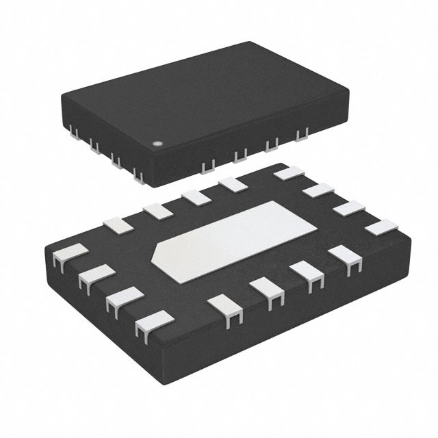


 工商网监
湘ICP备2023018690号
工商网监
湘ICP备2023018690号
