RoHS
YJD25N10A
COMPLIANT
N-Channel Enhancement Mode Field Effect Transistor
Product Summary
● VDS
● ID
● RDS(ON)( at VGS= 10V)
● RDS(ON)( at VGS= 4.5V)
● 100% EAS Tested
● 100% ▽VDS Tested
100V
25A
<52mohm
<56mohm
General Description
● Trench Power MV MOSFET technology
● Excellent package for heat dissipation
● High density cell design for low RDS(ON)
● Moisture Sensitivity Level 1
● Epoxy Meets UL 94 V-0 Flammability Rating
● Halogen Free
Applications
● DC-DC Converters
● Power management functions
● Backlighting
■ Absolute Maximum Ratings (TA=25℃unless otherwise noted)
Parameter
Symbol
Limit
Unit
Drain-source Voltage
VDS
100
V
Gate-source Voltage
VGS
±20
V
25
TC=25℃
Drain Current
A
ID
16
TC=100℃
Pulsed Drain Current A
IDM
100
A
45
TC=25℃
Total Power Dissipation
W
PD
18
TC=100℃
Single Pulse Avalanche Energy B
EAS
9.9
mJ
Thermal Resistance Junction-to-Case
RθJC
2.78
℃/ W
TJ ,TSTG
-55~+150
℃
Junction and Storage Temperature Range
■ Ordering Information (Example)
PREFERED P/N
PACKING
CODE
Marking
MINIMUM
PACKAGE(pcs)
INNER BOX
QUANTITY(pcs)
OUTER CARTON
QUANTITY(pcs)
DELIVERY MODE
YJD25N10A
F1/F2
YJD25N10A
2500
/
25000
13“ reel
1/7
S-E656
Rev.3.1,19-Mar-22
Yangzhou Yangjie Electronic Technology Co., Ltd.
www.21yangjie.com
�YJD25N10A
■ Electrical Characteristics (TJ=25℃ unless otherwise noted)
Parameter
Symbol
Conditions
Min
Drain-Source Breakdown Voltage
BVDSS
VGS= 0V, ID=250μA
100
Zero Gate Voltage Drain Current
IDSS
Typ
Max
Units
Static Parameter
Gate-Body Leakage Current
TJ=25℃
1
TJ=150℃
100
μA
VDS=100V,VGS=0V
IGSS
VGS= ±20V, VDS=0V
Gate Threshold Voltage
VGS(th)
VDS= VGS, ID=250μA
Static Drain-Source On-Resistance
RDS(ON)
Diode Forward Voltage
Maximum Body-Diode Continuous Current
VSD
V
±100
nA
1.8
3.0
V
VGS= 10V, ID=10A
43
52
VGS= 4.5V, ID=8A
46
56
IS=25A,VGS=0V
0.8
1.2
V
25
A
1.1
mΩ
IS
Dynamic Parameters
2071
Input Capacitance
Ciss
Output Capacitance
Coss
Reverse Transfer Capacitance
Crss
54
Total Gate Charge
Qg
51.4
Gate-Source Charge
Qgs
Gate-Drain Charge
Qgd
Reverse Recovery Chrage
Qrr
VDS=50V,VGS=0V,f=1MHZ
73
pF
Switching Parameters
VGS=10V,VDS=50V,ID=10A
9.1
nC
11.5
35.3
IF=10A, di/dt=100A/us
Reverse Recovery Time
trr
38
Turn-on Delay Time
tD(on)
10
Turn-on Rise Time
tr
Turn-off Delay Time
tD(off)
Turn-off fall Time
VGS=10V,VDD=50V, ID=2A
RGEN=3Ω
tf
19
ns
42
26
A.
Pulse Test: Pulse Width≤300us,Duty cycle ≤2%.
B.
C.
Tj=25℃, VDD=50V, VG=10V, L=0.5mH, IAS=6.3A
RθJA is the sum of the junction-to-case and case-to-ambient thermal resistance, where the case thermal reference is defined as
the soldermounting surface of the drain pins. RθJC is guaranteed by design, while RθJA is determined by the board design. The
maximum rating presented here is based on mounting on a 1 in 2 pad of 2oz copper.
2/7
S-E656
Rev.3.1,19-Mar-22
Yangzhou Yangjie Electronic Technology Co., Ltd.
www.21yangjie.com
�YJD25N10A
■ Typical Performance Characteristics
Figure 1. Output Characteristics
Figure 2. Transfer Characteristics
Figure 3. On-Resistance vs. Drain Current
and Gate Voltage
Figure 4. On-Resistance vs. Junction Temperature
Figure 5. Capacitance Characteristics
Figure 6. Gate Charge
3/7
S-E656
Rev.3.1,19-Mar-22
Yangzhou Yangjie Electronic Technology Co., Ltd.
www.21yangjie.com
�YJD25N10A
ID-Drain Current (A)
30
20
10
0
-50
0
50
100
150
Tc-Case Temperature (℃)
Figure 8. Maximum Continuous Drain Current
vs Case Temperature
Figure 7. Safe Operation Area
Figure 9. Normalized Maximum Transient Thermal Impedance
4/7
S-E656
Rev.3.1,19-Mar-22
Yangzhou Yangjie Electronic Technology Co., Ltd.
www.21yangjie.com
�YJD25N10A
Resistive Switching Test Circuit & Waveforms
Diode Recovery Test Circuit & Waveforms
Gate Charge Test Circuit & Waveform
Unclamped Inductive Switching (UIS) Test Circuit & Waveforms
5/7
S-E656
Rev.3.1,19-Mar-22
Yangzhou Yangjie Electronic Technology Co., Ltd.
www.21yangjie.com
�YJD25N10A
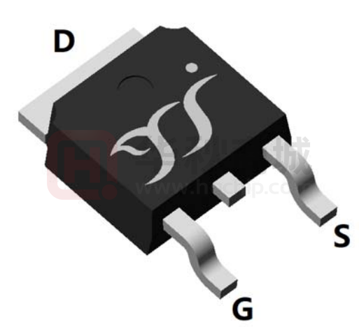
■ TO-252-B Package information
θ
TOP VIEW
SIDE VIEW
θ
BOTTOM VIEW
UNIT:mm
SUGGESTED SOLDER PAD LAYOUT
NOTE:
1.PACKAGE BODY SIZES EXCLUDE MOLD FLASH
AND GATE BURRS.
2.TOLERANCE 0.1mm UNLESS OTHERWISE
SPECIFIED.
3.THE PAD LAYOUT IS FOR REFERENCE
PURPOSES ONLY.
6/7
S-E656
Rev.3.1,19-Mar-22
Yangzhou Yangjie Electronic Technology Co., Ltd.
www.21yangjie.com
�YJD25N10A
Disclaimer
The information presented in this document is for reference only. Yangzhou Yangjie Electronic Technology Co., Ltd. reserves the
right to make changes without notice for the specification of the products displayed herein to improve reliability, function or design
or otherwise.
The product listed herein is designed to be used with ordinary electronic equipment or devices, and not designed to be used with
equipment or devices which require high level of reliability and the malfunction of with would directly endanger human life (such as
medical instruments, transportation equipment, aerospace machinery, nuclear-reactor controllers, fuel controllers and other safety
devices), Yangjie or anyone on its behalf, assumes no responsibility or liability for any damages resulting from such improper use
of sale.
This publication supersedes & replaces all information previously supplied. For additional information, please visit our website
http:// www.21yangjie.com , or consult your nearest Yangjie’s sales office for further assistance.
7/7
S-E656
Rev.3.1,19-Mar-22
Yangzhou Yangjie Electronic Technology Co., Ltd.
www.21yangjie.com
�


 工商网监
湘ICP备2023018690号
工商网监
湘ICP备2023018690号
