HiPerFETTM
Power MOSFETs
VDSS
IXFH/IXFM21N50
IXFH/IXFM/IXFT24N50
IXFH/IXFT26N50
N-Channel Enhancement Mode
High dv/dt, Low trr, HDMOSTM Family
OBSOLETE:
IXFM21N50
IXFM24N50
Test Conditions
Maximum Ratings
VDSS
TJ = 25°C to 150°C
500
V
VDGR
TJ = 25°C to 150°C; RGS = 1 MΩ
500
V
VGS
Continuous
±20
V
VGSM
Transient
±30
V
ID25
TC = 25°C
IDM
TC = 25°C, pulse width limited by TJM
21
24
26
84
96
104
21
24
26
A
A
A
A
A
A
A
A
A
30
mJ
5
V/ns
300
W
-55 ... +150
°C
TJM
150
°C
Tstg
-55 ... +150
°C
300
°C
TC = 25°C
EAR
TC = 25°C
dv/dt
IS ≤ IDM, di/dt ≤ 100 A/µs, VDD ≤ VDSS,
TJ ≤ 150°C, RG = 2 Ω
PD
TC = 25°C
TJ
TL
1.6 mm (0.062 in.) from case for 10 s
Md
Mounting torque
21N50
24N50
26N50
21N50
24N50
26N50
21N50
24N50
26N50
1.13/10
Weight
Nm/lb.in.
TO-204 = 18 g, TO-247 = 6 g
Symbol
Test Conditions
VDSS
VGS = 0 V, ID = 250 µA
VGS(th)
VDS = VGS, ID = 4 mA
IGSS
VGS = ±20 VDC, VDS = 0
IDSS
VDS = 0.8 • VDSS
VGS = 0 V
© 1999 IXYS All rights reserved
Characteristic Values
(TJ = 25°C, unless otherwise specified)
min. typ. max.
500
2
TJ = 25°C
TJ = 125°C
RDS(on)
500 V 21 A 0.25 Ω
500 V 24 A 0.23 Ω
500 V 26 A 0.20 Ω
trr ≤ 250 ns
Symbol
IAR
ID25
V
4
V
±100
nA
200
1
µA
mA
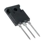
TO-247 AD (IXFH)
(TAB)
TO-268 (D3) Case Style
G
S
(TAB)
TO-204 AE (IXFM)
OBSOLETE
PACKAGE
TYPE
G
D
G = Gate,
S = Source,
D = Drain,
TAB = Drain
Features
• International standard packages
• Low RDS (on) HDMOSTM process
• Rugged polysilicon gate cell structure
• Unclamped Inductive Switching (UIS)
rated
• Low package inductance
- easy to drive and to protect
• Fast intrinsic Rectifier
Applications
• DC-DC converters
• Synchronous rectification
• Battery chargers
• Switched-mode and resonant-mode
power supplies
• DC choppers
• AC motor control
• Temperature and lighting controls
• Low voltage relays
Advantages
• Easy to mount with 1 screw (TO-247)
(isolated mounting screw hole)
• High power surface mountable package
• High power density
91525H (9/99)
�IXFH21N50
IXFM21N50
Symbol
Test Conditions
(TJ = 25°C, unless otherwise specified)
RDS(on)
Characteristic Values
Min. Typ.
Max.
VGS = 10 V, ID = 0.5 ID25
21N50
24N50
26N50
Pulse test, t ≤ 300 µs, duty cycle d ≤ 2 %
gfs
VDS = 10 V; ID = 0.5 ID25, pulse test
Ciss
Coss
Crss
VGS = 0 V, VDS = 25 V, f = 1 MHz
0.25
0.23
0.20
11
td(on)
tr
td(off)
tf
VGS = 10 V, VDS = 0.5 VDSS, ID = 0.5 ID25
RG = 2 Ω (External)
Qg(on)
Qgs
Qgd
VGS = 10 V, VDS = 0.5 VDSS, ID = 0.5 ID25
RthJC
RthCK
S
4200
450
135
pF
pF
pF
16
33
65
30
25
45
80
40
ns
ns
ns
ns
135
28
62
160
40
85
nC
nC
nC
0.25
0.42 K/W
K/W
Characteristic Values
(TJ = 25°C, unless otherwise specified)
Min.
Typ. Max.
Symbol
Test Conditions
IS
VGS = 0 V
21N50
24N50
26N50
21
24
26
A
A
A
ISM
Repetitive;
pulse width limited by TJM
21N50
24N50
26N50
84
96
104
A
A
A
VSD
IF = IS, VGS = 0 V,
Pulse test, t ≤ 300 µs, duty cycle d ≤ 2 %
1.5
V
250
400
ns
ns
µC
µC
A
A
t rr
QRM
IRM
IF = IS
-di/dt = 100 A/µs,
VR = 100 V
TJ =
TJ =
TJ =
TJ =
TJ =
TJ =
25°C
125°C
25°C
125°C
25°C
125°C
1
2
10
15
Note 1: Add "S" suffix for TO-247 SMD package option (ex: IXFH24N50S)
1
Dim.
2
Terminals:
1 - Gate
2 - Drain
3 - Source
Tab - Drain
3
Millimeter
Min.
Max.
Inches
Min.
Max.
A
A1
A2
4.7
2.2
2.2
5.3
2.54
2.6
.185
.087
.059
.209
.102
.098
b
b1
b2
1.0
1.65
2.87
1.4
2.13
3.12
.040
.065
.113
.055
.084
.123
C
D
E
.4
20.80
15.75
.8
21.46
16.26
.016
.819
.610
.031
.845
.640
e
L
L1
5.20
19.81
5.72
20.32
4.50
0.205
.780
0.225
.800
.177
∅P
Q
3.55
5.89
3.65
6.40
.140
0.232
.144
0.252
R
S
4.32
6.15
5.49
BSC
.170
242
.216
BSC
TO-204 AE (IXFM) Outline
Pins: 1 - Gate, 2 - Source, Case - Drain
Dim.
Millimeter
Min.
Max.
Inches
Min.
Max.
6.4
1.53
1.45
11.4
3.42
1.60
.250
.060
.057
.450
.135
.063
e
e1
10.67
5.21
11.17
5.71
.420
.205
.440
.225
L
11.18
12.19
.440
.480
3.84
3.84
4.19
4.19
.151
.151
.165
.165
A
A1
∅b
∅D
∅p
∅p1
TO-268 Outline
IXFH26N50
IXFM26N50
IXFT26N50
TO-247 AD (IXFH) Outline
Ω
Ω
Ω
21
(TO-247 Case Style)
Source-Drain Diode
IXFH24N50
IXFM24N50
IXFT24N50
q
22.22
30.15 BSC
.875
1.187 BSC
R
R1
12.58
3.33
13.33
4.77
.495
.131
.525
.188
s
16.64
17.14
.655
.675
Min. Recommended Footprint
IXYS reserves the right to change limits, test conditions, and dimensions.
IXYS MOSFETS and IGBTs are covered by one or more of the following U.S. patents:
4,835,592
4,850,072
4,881,106
4,931,844
5,017,508
5,034,796
5,049,961
5,063,307
5,187,117
5,237,481
5,486,715
5,381,025
�IXFH21N50
IXFM21N50
IXFH24N50
IXFM24N50
IXFT24N50
Fig. 1 Output Characteristics
50
50
7V
40
45
6V
35
TJ = 25°C
40
TJ = 25°C
ID - Amperes
ID - Amperes
Fig. 2 Input Admittance
VGS = 10V
45
30
25
20
5V
15
VDS = 10V
35
30
25
20
15
10
10
5
5
0
0
0
5
10
15
20
25
30
35
0
1
2
3
VDS - Volts
5
6
7
8
9
10
Fig. 4 Temperature Dependence
of Drain to Source Resistance
1.6
2.50
TJ = 25°C
2.25
1.4
1.3
VGS = 10V
1.2
VGS = 15V
1.1
RDS(on) - Normalized
1.5
RDS(on) - Normalized
4
VGS - Volts
Fig. 3 RDS(on) vs. Drain Current
1.0
2.00
1.75
ID = 12A
1.50
1.25
1.00
0.75
0.9
0
5
0.50
-50
10 15 20 25 30 35 40 45 50
-25
0
ID - Amperes
75
100 125 150
1.2
VGS(th)
26N50
BVDSS
1.1
BV/VG(th) - Normalized
25
24N50
21N50
15
10
5
0
-50
50
Fig. 6 Temperature Dependence of
Breakdown and Threshold Voltage
30
20
25
TJ - Degrees C
Fig. 5 Drain Current vs.
Case Temperature
ID - Amperes
IXFH26N50
IXFM26N50
IXFT26N50
1.0
0.9
0.8
0.7
0.6
-25
0
25
50
75
TC - Degrees C
© 1999 IXYS All rights reserved
100 125 150
0.5
-50
-25
0
25
50
75
TJ - Degrees C
100 125 150
�IXFH21N50
IXFM21N50
Fig.7
Gate Charge Characteristic Curve
100
VDS = 250V
IG = 10mA
100µs
ID - Amperes
7
VGE - Volts
10µs
Limited by RDS(on)
ID = 12.5A
8
IXFH26N50
IXFM26N50
IXFT26N50
Fig.8 Forward Bias Safe Operating Area
10
9
IXFH24N50
IXFM24N50
IXFT24N50
6
5
4
3
10
1ms
10ms
1
100ms
2
1
0
0.1
0
25
50
75
100 125 150 175 200
1
10
Gate Charge - nCoulombs
Fig.9
500
VDS - Volts
Capacitance Curves
Fig.10 Source Current vs. Source to Drain Voltage
50
4500
45
Ciss
4000
40
3500
ID - Amperes
Capacitance - pF
100
3000
f = 1 Mhz
VDS = 25V
2500
2000
1500
1000
5
10
15
20
25
20
TJ = 125°C
15
TJ = 25°C
5
Crss
0
0
30
10
Coss
500
35
0
0.00
25
0.25
0.50
VDS - Volts
0.75
1.00
1.25
1.50
VSD - Volt
Fig.11 Transient Thermal Impedance
Thermal Response - K/W
1
D=0.5
0.1
D=0.2
D=0.1
D=0.05
0.01 D=0.02
D=0.01
Single pulse
0.001
0.00001
0.0001
0.001
0.01
0.1
1
10
Time - Seconds
IXYS reserves the right to change limits, test conditions, and dimensions.
IXYS MOSFETS and IGBTs are covered by one or more of the following U.S. patents:
4,835,592
4,850,072
4,881,106
4,931,844
5,017,508
5,034,796
5,049,961
5,063,307
5,187,117
5,237,481
5,486,715
5,381,025
�


 工商网监
湘ICP备2023018690号
工商网监
湘ICP备2023018690号
